Article ID: 1003-6326(2005)03-0661-05
Growth of brass nanofilms sputtered on organic substrate
CHEN Zhen-xing(陈振兴)1, 2, WANG Ling-sen(王零森)1, HUANG Bai-yun(黄伯云)1
(1. State Key Laboratory for Powder Metallurgy, Central South University,
Changsha 410083, China;
2. School of Chemistry and Chemical Engineering, Central South University,
Changsha 410083, China)
Abstract: The growth of brass nanofilms sputtered on acrylics substrate was studied through experimental investigation of the effect of sputtering voltage, target-to-substrate distance, chamber pressure and sputtering time on the content, growth rate and surface morphology of brass nanofilms. The results show that compared with original brass target, Cu content in brass nanofilms changes by no more than 6.23%(mass fraction). High sputtering voltage and short target-to-substrate distance help to improve brass nanofilm deposition rate. There exists an optimal chamber pressure where deposition rate of nanofilm reaches the maximum. The key factor affecting surface morphology is the kinetic energy of sputtering particles. Low sputtering voltage, large target-to-substrate distance and low chamber pressure are very important for the formation of the high-quality brass nanofilms. The brass films prepared under the conditions of sputtering voltage 1.6kV, target-to-substrate distance 2.5cm, chamber pressure 10Pa and sputtering time 20min, possess following characteristics: smooth and uniform surface, thickness of 41nm and Cu content of 71.0%(mass fraction).
Key words: brass; nanofilm; sputtering; morphology; substrate CLC
number: TG135 Document code: A
1 INTRODUCTION
Metallic films have been widely used in chemical, catalytic and semiconductor industries[1-6]. Recently we have paid great attention to the uniform growth of brass film on organic substrate because brass film shows the possibility in manufacturing high-quality micro-mirror gold brass powder through vigorous stirring or ultrasonic treatment, in which film thickness will hardly change[6-9]. In traditional ball-milling process, high-quality micro-mirror gold brass powder is very hard to prepare[6, 8-10]. For high-quality flake brass powders, both thickness and smoothness are crucial. Usually, the appropriate thickness is 30-50nm[8-10]. On one hand, if the thickness is above 50nm, the mobility of flake powder may be low because of poor orientation, and moreover scattering effects may increase. Both low mobility and high scattering ultimately lead to a poor metallic characteristics(low brilliance, poor flop and coverage). On the other hand, if the thickness is less than 30nm, powders may become transparent, or very difficult to handle due to high agglomeration tendency[8, 9]. Now, physical vapor deposition(PVD) has been widely used to prepare metallic films[6-14]. To separate brass nanofilm from nanofilm/substrate heterostructure system, a releasable organic substrate is very important. The suitable releasable organic substrate are acrylics, cellulose or vinyl resins. So far, there is no report on sputtering of brass film on releasable organic substrate.
2 EXPERIMENTAL
The experiment was performed in a custom-designed sputtering chamber, which is shown in Fig.1. Acrylics was used as releasable organic substrate. Before deposition, acrylics was mechanically polished, cleaned by repeated Ar+ sputtering, and then annealed at 140℃ in order to remove impurities and obtain smooth substrate surface. The brass target was also polished and cleaned. Chamber pressure was measured with a vacuum gauge. The temperature of acrylics substrate was monitored with a chromel-alumel thermocouple, which was spot-welded on a Ta sheet attached to acrylics substrate surface. During the experiment, the temperature of the acrylics substrate was kept at 130℃.
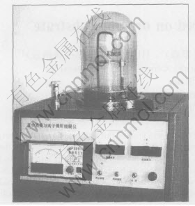
Fig.1 Sputtering device
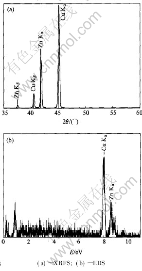
Fig.2 Composition analysis of brass target
The qualitative and quantitative analysis of brass target was performed with XRFS and EDS[15] and the results are shown in Fig.2. The Cu and Zn contents are respectively 73.8% and 26.2%(mass fraction).
To measure average thickness and Cu content of brass nanofilms, chemical analysis was put forward. After acrylics substrate had been resolved from brass/acrylics heterostructure system with alcohol, brass film was obtained through a centrifugal filter. Then, alloy film was dissolved with 6.5% nitric acid. The solution concentration was measured with ICP-AES. Both average thickness and content of brass film could be calculated according to the mass of Cu and Zn existing in the solution and the nanofilm area. AFM[15] was applied to investigate the surface morphology of the brass nanofilms.
3 RESULTS AND DISCUSSION
3.1 Cu content of brass nanofilms
The effects of sputtering voltage, target-to-substrate distance, chamber pressure and sputtering time on Cu content in brass nanofilms are shown in Fig.3. Fig.3(a) shows that an increase in the sputtering voltage from 1.0kV to 2.0kV increases the Cu content from 69.2% to 77.4%. Because of selective sputtering, Zn is sputtered prior to Cu under low voltage (lower than 1.6kV), and then brass nanofilms with relative low Cu content are prepared. However, under high voltage (higher than 2.0kV), Cu is sputtered prior to Zn, and then brass nanofilms with relative high Cu content are deposited. Target-to-substrate distance and sputtering time nearly have no effect on Cu content(Figs.3(b) and (d)). Chamber pressure affects Cu content to some extent Fig.3(c)). For example, when chamber pressure is 5Pa, Cu content will be 2.4% higher than that of brass target. However, at high chamber pressure, Cu content will decrease slightly. Therefore, through the control of sputtering voltage, target-to-substrate distance, chamber pressure and sputtering time, brass nanofilms with almost the same content as brass target can be steadily deposited.
3.2 Growth rate of brass nanofilms
The effects of sputtering voltage, target-to-substrate distance, chamber pressure and sputtering time on the growth rate of brass films are shown in Fig.4. Fig.4(a) shows that the growth rate of brass films increases with the increase in the sputtering voltage. At high sputtering voltage, large amount of Ar atoms in bulk gas will ionize and turn into sputtering ions Ar+, which provides large collision odds on the target surface. At the same time, high voltage will improve the kinetic energy of Ar+, and then much more energy will be transferred to target atoms. These factors help the atoms to escape from target surface into bulk gas, and then improve the growth rate of brass nano-films. However, at high voltage, arc can easily be formed and nanofilms may blacken due to high temperature. Of course, sputtering voltage cannot be too low. Otherwise, effective bombing will not be realized. At low energies, just above threshold, the incident ions barely have enough energy to cause physical sputtering, and much of their energy
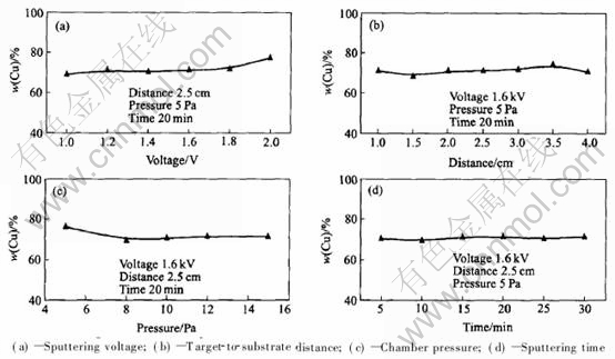
Fig.3 Effects of process conditions on Cu content in brass nanofilms
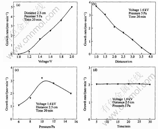
Fig.4 Effects of sputtering voltage(a), target-to-substrate distance(b),chamber pressure(c) and sputtering time(d) on growth rate of brass films
is dissipated as heat or, of course, carried away by the reflected atom. Very little commercial sputter deposition and only very specialized sputter etch are performed in this region since the sputtering rate per unit incident power is small. Actually, film thickness will also increase with the increase of voltage. Fig.4(b) shows that the film growth gradually decreases because more collisions will take place in bulk gas region, which decreases the kinetic energy and then increases scattering quotient with increasing the target-to-substrate distance. Fig.4(c) shows that when chamber pressure is lower than 10Pa, larger growth rate can be reached with the increase in chamber pressure; and growth rate will reach the maximum value at 10Pa. Then, growth rate will decrease gradually. On one hand, with the increase of pressure, more collision odds and then more sputtering atoms will be created, which improves the growth of brass nanofilms. On the other hand, a higher pressure in the chamber will greatly shorten the mean free path of Ar+ and sputtering atoms so that the kinetic energy of sputtering atoms and then usefulness of growth rate will depress because of much scattering. Fig.4(d) shows that sputtering time has little effect on growth rate of brass nanofilms. When sputtering time increases from 5min to 30min, the thickness of brass film increases from 10nm to 60nm.
3.3 Surface morphology of brass nanofilms
The three-dimensional morphology of brass film, which was detected by AFM, is shown in Fig.5. It reveals that if sputtering voltage increases, roughness of alloy film surface will increase[CM(22](Fig.5(b)). In other words, low sputtering volt-[CM)]age will result in smooth films. On one hand, at high sputtering voltage, the deposition rate is large so that some of deposition atoms cannot diffuse and distribute on acrylics surface on time. On the other hand, at high sputtering voltage, because of high kinetic energy, sputtering atoms may provide much probability of damage or defects on alloy film. For short target-to-substrate distance, the nanofilm surface may become more rough or uneven(Fig.5(c)) because some of nanofilm surfaces probably break under the collision of sputtering atoms with high kinetic energy. At high pressure, the nanofilm surface may turn to be more rough(Fig.5(d)) because the number of sputtering atoms become large so that some of the deposition atoms cannot diffuse and distribute on time. Therefore, the key factor affecting morphology of brass nanofilm surface is the kinetic energy of the sputtering atoms. High kinetic energy is useful for rapid deposition, but it prevents atoms from diffusing and distributing uniformly on time, and then results in uneven nanofilm. So, it is important to increase substrate temperature in order to improve diffusion and distribution on acrylics surface. For deposition of high-quality smooth alloy film, low sputtering voltage, large target-to-substrate distance and low chamber pressure are necessary. For brass film, optimal conditions are sputtering volt-
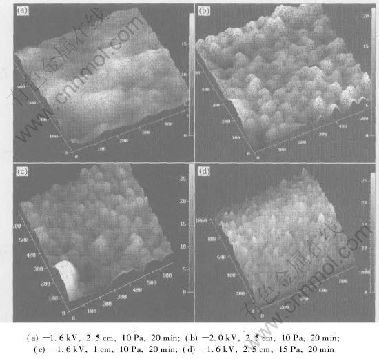
Fig.5 Three-dimensional AFM images of brass nanofilms prepared under different conditions
age 1.6kV, target-to-substrate distance 2.5cm, chamber pressure 10Pa and sputtering time 20min. Two-dimensional AFM image(Fig.(6)) of brass film prepared under the optimal condition shows uniform distribution. Such brass film presents the following characteristics: smooth and uniform surface, Cu content of 71.0% and average thickness of 41nm.
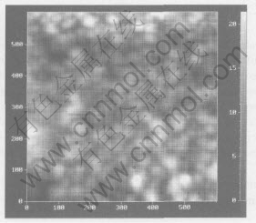
Fig.6 Two-dimensional AFM image of brass nanofilm
4 CONCLUSIONS
1) Cu content of brass nanofilms deposited on acrylics substrate(130℃) varies in the range of 69.2%-77.4%(mass fraction). If the sputtering condition is well controlled, brass nanofilms with nearly the same content as brass target can be steadily prepared.
2) With the augment of sputtering voltage, growth rate of brass nanofilms will increase. The growth rate is linear decreasing function of the target-to-substrate distance. There exists an optimal chamber pressure where growth rate reaches the maximum value. When chamber pressure is lower than 10Pa, growth rate will be improved with the increase of chamber pressure.
3) Both high sputtering voltage and short target-to-substrate distance will result in more damages or defect on brass film. Rough surface will be deposited at high chamber pressure because of much scattering and cavities.
4) High-quality brass nanofilm can be prepared on acrylics substrate under the conditions of sputtering voltage 1.6kV, target-to-substrate dis-[CM(22]tance 2.5cm, chamber pressure 10Pa and sputter-[CM)]ing time 20min. The resulting 41nm-thick brass film is characterized by smooth and uniform surface and Cu content of 71.0%(mass fraction).
REFERENCES
[1]Ohnuma S, Masumoto T. High frequency magnetic properties and GMR effect of nano-granular magnetic thin films [J]. Scripta Materialia, 2001, 44(8-9): 1309-1313.
[2]Roaul W, Marguerte J, Jean L L, et al. Preparation of optical quality Zn-Cd-Te thin films by vacuum evaporation [J]. Applied Optics, 1998, 37(13): 2881-2882.
[3]Sung T K, Hyun H K, Hyun I K, et al. Effect of activation of oxygen by electron cyclotron resonance plasma on the incorporation of Pb in the deposition of Pb(Zr, Ti)O2 films by DC magnetron sputtering [J]. Japanese Journal of Applied Physics, 1997, 36(5): 3379-3382.
[4]Mammana A P, Torriani I L, Silveira M A, et al. Characterization of Ta thin films obtained by dc sputtering [J]. Vacuum, 1990, 41(6): 1403-1404.
[5]Scherer M. Reactive alternating current magnetron sputtering of dielectric layer [J]. Journal of Vacuum Science & Technology, 1992, 10(4): 1772-1776.
[6]CHEN Zhen-xing, HUANG Qiao-ping, LU Bi-zhi, et al. Research on brass gold powder and trend [J]. Packing Engineering, 2003, 24(4): 7-9.(in Chinese)
[7]CHEN Zhen-xing, WAGN Ling-sen. Plate-like Brass Nanograde Powder and its Manufacture Method [P]. CN200310110526.7, 2003.(in Chinese)
[8]CHEN Zhen-xing. Special Powders [M]. Beijing:Chemistry Industry Press, 2004.(in Chinese)
[9]HUANG Qiao-ping. Sputtering Growth of Brass Nanograde Films [D]. Changsha: Central South University, 2004.(in Chinese)
[10]James J D, Wilshire B. Laboratory simulation of commercial Cu/Zn alloy flake manufacture [J]. Powder Metallurgy, 1990, 33 (3): 247-249.
[11]Nizar B, Khaled D, Jean L B. Plasma and wet oxidation of (63Cu37Zn) brass [J]. Materials Chemistry and Physics, 2002, 73(15): 235-241.
[12]Mentkowski V S. Trends in sputtering [J]. Progress in Surface Science, 2000, 64(1): 1-59.
[13]Facako S, Dekorsy T, Koerdt C, et al. Formation of ordered nanoscale semiconductor dots by sputtering [J]. Science, 1999, 285: 1551-1553.
[14]Galdikas A, Pranevicius L. Surface composition changes of ternary alloys in the non-steady state regime of preferential sputtering [J]. Nuclear Instruments and Methods in Physics Research B, 2000, 164-165: 868-872.
[15]Morton R. Nano-Surface Chemistry [M]. New York: Marcel Dekker Inc, 2001.
(Edited by YANG Bing)
Foundation item: Project(20276080) supported by the National Natural Science Foundation of China; Project(2003034464) supported by China Postdoctoral Science Foundation Received date: 2004-05-10; Accepted date: 2004-12-20
Correspondence: CHEN Zhen-xing, Professor, PhD; Tel: +86-731-8876780; E-mail: chenzx@mail.csu.edu.cn