Sputter-deposited TiNiPd alloy films on Si wafer
QIAN Shi-qiang(Ǯʿǿ)1, 2, WU Jian-sheng(�⽨��)1
(1. School of Materials Science and Engineering, Shanghai Jiaotong University, Shanghai 200030, China;
2. School of Materials Engineering, Shanghai University of Engineering Science, Shanghai 200336, China)
Abstract: Amorphous thin films of Ti51.78Ni22.24Pd25.98 alloys were deposited onto n-type(100) Si wafer by radio frequency magnetron sputtering. From X-ray diffraction patterns, the crystallization temperature of thin film on Si wafer is found to be higher than 553.1��. The film heated at 750�� for 1h quite crystallizes along with some precipitation, but at 550�� it partially crystallizes. With heating for 50h at 450�� before crystallization, the film will contain more B19�� phases after succeeding heat-treatment at 650��, but less B19�� phases after 750�� treatment are found. The fracture morphology of the film heated at 550�� shows a flat pattern with more steps, whereas that of the film preparing at 750�� displays a well-defined fine granulation structure. 550��-heated film is harder than as-deposited film because of good cohesion between film and Si wafer.
Key words: TiNiPd; thin film; sputter deposition; crystallization; martensitic transformation; fracture morphology; nano-hardness CLC number: TG139. 6
Document code: A
1 INTRODUCTION
Shape memory thin film is regarded as one of the most promising materials for micro-electro-mechanical system(MEMS)[1-3] because it provides large output force per unit volume and works as both the structural and the functional components. Deposited TiNi thin films have been intensely investigated and are widely used at present. TiNiPd high-temperature shape memory thin films exhibit higher phase transformation temperature compared with the usual ones[4, 5], and respond quickly due to the efficient thermal exchange, thus have received great attentions for fabricating micro-actuators.
It is important to study the phase transformation behavior, because the shape memory effect is generally realized through the transformation process. In Ti50Ni50-xPdx alloys, phase transformation has been studied by many authors[6-8]. It is known that the transformation sequence is changed from B2-B19�� through B2-R-B19��, to B2-B19-B19��, and then into B2-B19 as the Pd content increases. Here, B2 refers to the high temperature austenite phase (CsCl type structure), while B19 and B19�� to the orthorhombic and monoclinic martensites, respectively. According to our previous work concerning the bulk Ti50+xPd30Ni20-x alloys, both the B2-B19 and the B2-B19-B19�� transformations can be retained through various heat treatments[9]. In the films sputtered from (TiPd)50(TiNi)50 target[10], it is believed that a mixture of B19 and B19�� phases would exist at low temperature. It is therefore necessary to obtain a clear understanding of the effects of heat treatment on microstructure of TiNiPd thin films. Thin film sputter-deposited on Si wafer was proposed for fabricating microactuators or micro-devices used in MEMS[11], so that the film on Si wafer was emphasized in this paper.
2 EXPERIMENTAL
A Ti50.6Pd30Ni19.4 ingot was made by arc melting 99%Ti, 99%Ni and 99.9%Pd on a water-cooled copper mould under a controlled protective argon atmosphere. The ingot was remelted four times, and then homogenized in vacuum at 1000�� for 5h. Finally, the ingot was hot-rolled into 1mm-thick plate at 800��. A target with gauge size of d78mm��1mm was spark eroded followed by mechanical polishing. Films were formed by radio frequency(r.f.) magnetron sputtering onto unheated silicon wafer substrates in Ar gas at 0.3Pa. The base pressure in the deposition system was of the order 10-4Pa, r.f. power was 200W and the substrate-target distance was about 50mm. The sputtering time was 30min and the film thickness was about 2��m. The as-deposited thin films on Si wafer were protected by Ti plate for crystallization at 550��, 650��, 750�� for 1h, respectively, in evacuated quartz capsules, and some of them were pre-crystallized at 450�� for 5 or 50h previously.
Energy-dispersive X-ray microanalysis(EDX) was employed to measure the compositions of the film using PHILIPS SEM515 energy spectrometer. X-ray diffraction(XRD) measurements were performed using a Rigaku Dmax-rc diffractometer with a CuK�� radiation. The crystallizing point of the thin films was determined by differential scanning calorimetry(DSC) using a NETZSCH DSC 404 calorimeter. The specimen peeled from Si wafer weighed 1.4mg and the heating / cooling rate for the measurement was 40��/min. In order to observe the fractograph of the films under different heat treatment conditions, HITACH S2700 scanning electron microscope(SEM) was used. The nano-hardness of the films before and after crystallizing was measured by CSM Nano-Hardness-Tester NHT S/N: 06-0140. The maximum load 10mN was applied to the films on Si wafer by linear loading. The loading/unloading rate was 20mN/min and Poisson��s ratio of the films was assumed as 0.25.
3 RESULTS AND DISCUSSION
3.1 Film compositions
The Ti, Ni and Pd contents in the film on Si wafer are listed in Table 1. They were inhomogeneous in many micro-regions. The maximum content of Ni is at the center of the Si wafer, but the minimum contents of Ti or Pd is there. The case is inversed at the edge of the Si wafer. The variation ranges of Ti, Ni and Pd contents all exceed 2%(molar fraction). The distance between substrate and target strongly influences the deposition rate and uniformity of composition on the substrate surface. Shortening the distance can enhance the deposition rate, while degenerate the uniformity of composition[12]. It has been found that the transformation temperature of TiNi-based alloy is very sensitive to the Ti content and can be changed greatly even by a slight fluctuation of the Ti content less than 1%(molar fraction)[13]. Obviously, the variation in Ti, Ni and Pd contents will cause a various transformation temperature distribution in micro-region in the film. In order to eliminate the inhomogeneity of the film compositions, a long-time or a high-temperature treatment is necessary.
Because Ti, Ni and Pd elements are very different in their sputtering rates and adsorption coefficients at substrate surface, the film compositions are deviated from those of Ti50.6Ni19.4Pd30 alloy tar-
Table 1 Compositions of target and deposited film on Si wafer(molar fraction, %)
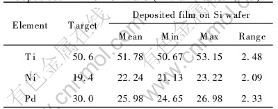
get. It can be found from Table 1 that 1.18% for Ti and 2.84% for Ni higher but 4.02%(molar fraction) for Pd lower than those of the target made of Ti50.6Pd30Ni19.4 ingot. Generally, in TiNi films the Ti content is lower but Ni content is higher than that of the target because the sputtering yield(number of atoms sputtered per Ar ion) for Ti is lower than that for Ni. In ternary alloy TiNiPd films, it is Pd content not Ti content that is far lower than that of the target. The addition of Pd in TiNiPd alloy is to hoist the phase transformation temperature Ms and/or As. Insufficient Pd in the film induces the Ms and/or As of the film to the temperature below that of the target, at which the film is fabricated. Unlike making TiNi alloy film, in order to obtain an ideal compositions in TiNiPd film with higher transformation temperature, the target must be enriched with Pd not Ti.
3.2 Film crystallization
The XRD patterns reveal that the sputter-deposited film on Si wafer is in amorphous or non-crystalline state and for crystallization the film should be heated at the temperature over crystallizing point. Fig.1 shows the heat flow curves of the film heated from 100�� to 1000�� and then cooled to 300��. The heat-cooling cycle is run again when cooling the film to room temperature after first cycle. An exothermic peak appears at the heat stage of the first cycle but disappears at the second one, which implies that the exothermic peak results from film��s crystallization because the film is in amorphous state at the beginning of first cycle but in crystalline state at the second one. The peak temperature(553.1��) is the crystallizing point of the film. Fig.2 shows the XRD patterns of the film as deposited and heated at 550�� for 5h. Fig.3 and Fig.4 show the XRD patterns of the films heated at 650�� and 750�� respectively. Some XRD patterns of the films undergoing pre-crystallization at 450�� for 50h before crystallization are also shown in Fig.3 and Fig.4. According to the XRD patterns, the crystallinity of the films is strongly dependent on the crystallization temperature. During heating below 500��, the films have little change and retain amorphous structure, in whose XRD pattern appears diffuse scattering. The film heated at 550��, in spite of being or not being pre-crystallized at 450��, undergoes some crystallization and only small part in the film is crystallized. The XRD pattern remains diffuse scattering shape mostly but some diffraction peaks appear, which indicates some crystals form. Up to 650�� the films basically crystallize and the XRD pattern shows some sharp diffraction peaks but a little diffuse scattering is residual. The film heated at 750�� completes crystallization entirely. The treatment of pre-crystallization at 450�� does not have more effects on the crystallinity of the films.
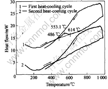
Fig.1 DSC curves of film measured during heating from 100�� to 1000�� then cooling to 300��

Fig.2 XRD patterns of films as-deposited and crystallized at 550�� for 5h
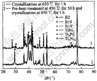
Fig.3 XRD patterns of film crystallized at 650�� for 1h with and without pre-heat-treatment
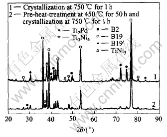
Fig.4 XRD patterns of films crystallized at 750�� for 1h with and without pre-heat-treatment
According to the DSC result, the film heated over 550�� will be in crystalline state but the fact revealed by XRD is not so. This disaccordance is related to Si wafer. The film used in DSC measure is free-standing but the films heated for crystallizing are attached to n-type (100) Si wafer. The structure of Si wafer influences the crystallization of the film adhered on it. When films are heated, a preferred orientation linked to single crystal Si wafer is promoted so that crystallization is impeded. From XRD pattern of the film heated below 550��, a weak peak at about 2��=70�� corresponding to Si {400} appears. The atoms cohered to Si periodic lattice will move hard for forming other lattices, which leads to the films on Si wafer crystallizing completely at the temperature higher than normal crystallizing point.
3.3 Phase constitution
According to the XRD results, after crystallization, chief phases in the TiNiPd film on Si wafer are Ti-Ni-Pd ternary alloy phases: B2 austenite phase, B19 orthorhombic martensite and B19�� monoclinic martensite at room temperature. Although B2 is high temperature phase, it exists at room temperature whether the film crystallizes at 550�� or at 750��. Fig.2 instructs that there is many B2 phase in the film heated at 550�� for 5h. Fig.3 and Fig.4 also instruct that some B2 phases appear in the film heated at 650�� or 750��. When the transformation from amorphous phase to crystal occurs in the film at high temperature, the first crystal phase formed in the film is B2 austentite phase which is the equilibrium phase and is stable at that temperature. At enough low temperature, the B2 phase formed at high temperature changes to B19 or B19�� martensite which is the equilibrium phase at room temperature. At the temperature below 550�� the crystallization in the film is not completed and the B2 phase formed will not change to martensite and exists still at room temperature because non-uniform component in the B2 phase does not meet with atoms co-operation required for forming martensite. The B2 phase formed at the temperature high enough is homogeneous and easily changes to B19 or B19�� martensite. But a little B2 phase remains at room temperature owing to non-uniform microdistribution.
Fig.3 and Fig.4 clearly show that most martensites in the films are B19 orthorhombic martensite and a little part is B19�� monoclinic martensite. The Pd-content in the film affects the contents of B19 or B19�� and the type of phase transformation[13]. When the Pd-content in the film is below 10%(molar fraction), B2-B19-B19�� two-stage phase transformation will happen as temperature falls and B19�� monoclinic martensite chiefly forms in the film at room temperature. B19 and B19�� will coexist at room temperature when B19-B19�� transformation is incomplete. When the Pd-content in the film is over 15%(molar fraction), only B2-B19 one-stage phase transformation happens and B19 orthorhombic martensite chiefly exists at room temperature. In this paper, the Pd-content in the film reaches 25%(molar fraction) so that there is more B19 phases in the crystallized film. The precipitates formed in crystallization will change Pd-content of the matrix. Fig.3 and Fig.4 show that TiNi3, Ti2Pd and Ti3Ni4 precipitates appear in the films. The formation of Pd precipitation Ti2Pd will reduce Pd-content in the matrix and leads to B19�� forming, but the formation of Ni precipitates TiNi3 or Ti3Ni4 will do inversely. From Fig.3 it is found that pre-crystallization at 450�� impedes Ti3Ni4 formation in the film heated at 650��, as a result, B19�� peaks appear; but from Fig.4 pre-crystallization slows down Ti2Pd formation so that less B19�� forms in the film after the second heat treatment at 750��.
3.4 Electron fractography
By SEM the fractography of the films formed with Si substrate broken by bending or compressing or colliding etc is observed. The effect of heating temperature for crystallization on the fractography is found. Fig.5 shows the cross-sectional SEM micrographs of the films on Si wafer crystallized at different temperatures. The fracture of as-deposited films exhibits a dense structure or flat pattern with some steps and no clustered columnar structure is observed[14]. The film heated at low temperature (550��, 1h) also shows the same dense structure but with far more steps (Fig.5(a)), whereas the film prepared at high temperature(750��, 1h) reveals a well-defined fine granulation structure and no flat pattern is seen(Fig.5(b)). A striated pattern is observed evidently but the fine grain builds up the striae. The fine granulation structure suggests that grains are relatively perfect and appears to be caused by the crack propagating along grain or martensite boundary. The grain and martensite formation will inherit or develop columnar structure that is innative in sputter-deposited films[15], which weakens column boundary and induces crack to propagate, so the striated pattern forms at fracture surface as shown in Fig.5(b). The amorphous state in film as-deposited without weak boundary resists crack propagating so that the flat pattern forms when fracture happens. The film heated at 550�� undergoes imperfective crystallization and retains amorphous state mostly, but atom relaxation in the film at that temperature abates film��s resistance for crack propagating so that more steps appear at the fracture surface as shown in Fig.5(a).
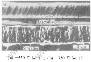
Fig.5 Cross-sectional SEM micrograph of films on Si wafer
3.5 Nano-hardness
Fig.6 shows nanoindentation curves measured for nano-hardness HV of the films as-deposited and heated at 550��. The value of nano-hardness HV is achieved from the curves by equation: HV=Fmax/(9.81Ac��hc). Here Fmax is the maximum load, Ac and hc are contact area and depth of indentation corresponding to maximum load respectively. The nano-hardness is 774 in the as-deposited film but increased to 831 in the film heated at 550�� because of atom relaxation and some intergranular formed in the film. As shown in Fig.6, two curves are coincident entirely at the loading stage but no overlap appears at the unloading stage. Fig.6 indicates that curve 1 drops quickly with load decreasing and ends up at depth of 179.1nm, but curve 2 drops slowly and ends up at 153.6nm, which instructs that the film as-deposited recovers less and retains more deformation after unloading, but the film heated at 550�� recovers more and reserves less deformation. That is, the film heated at 550�� is harder than the film as-deposited. Furthermore, it is found that unlike as-deposited one, the film will hardly be peeled out from Si substrate after heat treatment at 550�� and will exhibit good cohesion with Si wafer. These are attributed to the chemical reactions between TiNi(Pd) and Si which completes in 30min treatment at 525��[16].
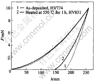
Fig.6 Nanoindentation curves measured for nano-hardness HV
4 CONCLUSIONS
1) The films on Si wafer crystallize completely at the temperature higher than normal crystallizing point. The crystallinity of the films is strongly dependent on the crystallizing temperature.
2) At room temperature, B19 orthorhombic martensite is the chief phase and some B2 and B19�� phases coexist in the crystallized films. Pre-crystallization at 450�� for 50h will accelerate B19�� phase formation in the film after succeeding heat-treatment at 650�� but slow it down after heat treatment at 750��.
3) The fracture morphology of the film heated at 550�� is different from that of the film prepared at 750��. The former shows a flat pattern with more steps whereas the latter displays a well-defined fine granulation structure.
4) The film heated at 550�� is harder than as-deposited one because of good cohesion between film and Si wafer.
REFERENCES
[1]Otsuka K, REN Xiao-bing. Recent developments in the research of shape memory alloys [J]. Intermetallics, 1999, 7(5): 511-528.
[2]WU Ting-bin, JIANG Bo-hong, QI Xuan. Advancement in application research on NiTi shape memory thin films [J]. The Chinese Journal of Nonferrous Metals, 2001, 11(S2): 272-276.(in Chinese)
[3]Kohl M, Dittmann D, Quandt E, et al. Shape memory microvalves based on thin films or rolled sheets [J]. Materials Science and Engineering A, 1999, 273-275: 784-788.
[4]Quandt E, Halene C, Holleck H, et al. Sputter deposition of TiNi,TiNiPd and TiPd films displaying the two-way shape-memory effect [J]. Sensors and Actuators A, 1996, 53: 434-439.
[5]Sawaguchi T, Sato M, Ishida A. Microstructure and shape memory behavior of Ti51.2(Pd27.0Ni21.8) and Ti49.5(Pd28.5Ni22.0) thin films [J]. Materials Science and Engineering A, 2002, 332: 47-55.
[6]Matveeva N M, Kovneristyi Y K, Savinov A S, et al. Martensitic transformations in the TiPd-TiNi system [J]. J Physique, 1982, 43: 249-251.
[7]Lo Y C, Wu S K, Wayman C M. Transformation heat as function of ternary Pd additions in Ti50Ni50-xPdx alloys with x:20-50at% [J]. Scripta Metall Mater, 1990, 24: 1571-1576.
[8]Lo Y C, Wu S K. Compositional dependence of martensitic transformation sequence in Ti50Ni50-xPdx alloys with x��15at.% [J]. Scripta Metall Mater, 1992, 27: 1097-1102.
[9]Tian Q C, Wu J S. Phase transformation behaviour and microstructure of Ti51Pd30Ni19 alloy [J]. Z Metakd, 2001, 5: 436-440.
[10]Mathews S, Li J, Su Q, et al. Martensitic transformation in thin-film (TiPd)50(TiNi)50 [J]. Phil Mag Lett, 1999, 79: 265-272.
[11]Miyazaki S, Ishida A. Martensitic transformation and shape memory behavior in sputter-deposited TiNi-based thin films [J]. Materials Science and Engineering A, 1999, 273-275: 106-133.
[12]Ohta A, Bhansali S, Kishimoto I, et al. Novel fabrication technique of TiNi shape memory alloy film using separate Ti and Ni targets [J]. Sensors and Actuators A, 2000, 86: 165-170.
[13]Tian Q C, Wu J S. The elastic behavior of Ti50+xPd30-Ni20-x high-temperature shape memory alloys [J]. Acta Metall Sinica, 2001, 6: 658-664.
[14]Chu J P, Lai Y W, Lin T N, et al. Deposition and characterization of TiNi-base thin films by sputtering [J]. Materials Science and Engineering A, 2000, 277: 11-17.
[15]Gadieu F J, Chencinski N. Selective thermallization in sputting to produce high Tc films [J]. IEEE Trans Magn, 1975, 11: 227-230.
[16]WEN Shu-lin. Microstructure and mechanical properties of TiNi SME thin film [J]. Journal of Chinese Electron Microscopy Society, 2002, 3: 294-300.
(Edited by YANG Bing)
Foundation item: Project(20020248037) supported by the Specialized Research Fund for the Doctoral Program of Higher Education of China; Project(02DJ14042) supported by the Science and Technology Commission of the Shanghai Municipal Government, China
Received date: 2004-11-05; Accepted date:2005-03-08
Correspondence: QIAN Shi-qiang, Associate Professor, PhD; Tel: +86-21-54772680; Fax: +86-21-54772680; E-mail: qsqli@online.sh.cn

