Design of area and power efficient radix-4 DIT FFT butterfly unit using floating point fused arithmetic
��Դ�ڿ������ϴ�ѧѧ��(Ӣ�İ�)2016���7��
�������ߣ�Prabhu E Mangalam H Karthick S
����ҳ�룺1669 - 1681
Key words��floating-point arithmetic; floating-point fused dot product; Radix-16 booth multiplier; Radix-4 FFT butterfly; fast fourier transform; decimation in time
Abstract: In this work, power efficient butterfly unit based FFT architecture is presented. The butterfly unit is designed using floating-point fused arithmetic units. The fused arithmetic units include two-term dot product unit and add-subtract unit. In these arithmetic units, operations are performed over complex data values. a modified fused floating-point two-term dot product and an enhanced model for the Radix-4 FFT butterfly unit are proposed. The modified fused two-term dot product is designed using Radix-16 booth multiplier. Radix-16 booth multiplier will reduce the switching activities compared to Radix-8 booth multiplier in existing system and also will reduce the area required. The proposed architecture is implemented efficiently for Radix-4 decimation in time (DIT) FFT butterfly with the two floating-point fused arithmetic units. The proposed enhanced architecture is synthesized, implemented, placed and routed on a FPGA device using Xilinx ISE tool. It is observed that the Radix-4 DIT fused floating-point FFT butterfly requires 50.17% less space and 12.16% reduced power compared to the existing methods and the proposed enhanced model requires 49.82% less space on the FPGA device compared to the proposed design. Also, reduced power consumption is addressed by utilizing the reusability technique, which results in 11.42% of power reduction of the enhanced model compared to the proposed design.
J. Cent. South Univ. (2016) 23: 1669-1681
DOI: 10.1007/s11771-016-3221-y

Prabhu E1, Mangalam H2, Karthick S3
1. Department of Electronics and Communication Engineering, Amrita School of Engineering,
Coimbatore, Amrita Vishwa Vidyapeetham, Amrita University, India;
2. Department of Electronics and Communication Engineering, Sri Krishna College of Engineering and Technology,
Coimbatore-641008, Tamilnadu, India;
3. Department of Electronics and Communication Engineering,Bannari Amman Institute of Technology, Sathyamangalam-638401, Tamilnadu, India
 Central South University Press and Springer-Verlag Berlin Heidelberg 2016
Abstract: In this work, power efficient butterfly unit based FFT architecture is presented. The butterfly unit is designed using floating-point fused arithmetic units. The fused arithmetic units include two-term dot product unit and add-subtract unit. In these arithmetic units, operations are performed over complex data values. a modified fused floating-point two-term dot product and an enhanced model for the Radix-4 FFT butterfly unit are proposed. The modified fused two-term dot product is designed using Radix-16 booth multiplier. Radix-16 booth multiplier will reduce the switching activities compared to Radix-8 booth multiplier in existing system and also will reduce the area required. The proposed architecture is implemented efficiently for Radix-4 decimation in time (DIT) FFT butterfly with the two floating-point fused arithmetic units. The proposed enhanced architecture is synthesized, implemented, placed and routed on a FPGA device using Xilinx ISE tool. It is observed that the Radix-4 DIT fused floating-point FFT butterfly requires 50.17% less space and 12.16% reduced power compared to the existing methods and the proposed enhanced model requires 49.82% less space on the FPGA device compared to the proposed design. Also, reduced power consumption is addressed by utilizing the reusability technique, which results in 11.42% of power reduction of the enhanced model compared to the proposed design.
Key words: floating-point arithmetic; floating-point fused dot product; Radix-16 booth multiplier; Radix-4 FFT butterfly; fast fourier transform; decimation in time
1 Introduction
For several years, a lot of researchers have shown their attention towards floating-point fused arithmetic implementation on FPGAs [1]. The IBM RISC (reduced instruction set computer) system (RS/6000) floating- point unit (FPU) [2] indicates a second-generation RISC CPU architecture and an implementation that is capable of largely improving the floating-point performance and accuracy. They denoted a unified floating-point multiply-add-fused unit (MAF) that can decrease the latency, rounding errors and chip busing. In addition, the number of adders/normalizers used can be reduced as well. This unit has achieved a peak execution rate of 50 MFLOPS (million floating-point operations per second) with a 25-MHz clock frequency and was able to maintain this rate even in complex programs. But Hokenek et al [3] have explained about a 440000-transistor second-generation RISC floating-point chip in. The pipeline latency obtained with this architecture was two cycles only and each cycle yielded a double-precision result. An improvement in the system throughput and accuracy was also achieved with the utilization of a floating-point multiply-add-fused unit, which performed double-precision accumulate as a two-cycle pipelined execution with only one rounding error. As the cycle time (40 ns) was competitive with other CMOS RISC systems, the floating-point performance gets enlarged to the range of bipolar RISC systems (7.4-13 MFLOPS LINPACK). Leading zero anticipation has enabled the two-cycle pipeline possible through nearly reducing the extra post normalization time and the factors that has resulted in reduced overall system potential. Partial decode shifters have permitted complete time sharing for the multiply and data alignment.
An efficient implementation of a conventional floating point multiplier that has aided the IEEE 754-2008 binary interchange format was introduced in by Al-Ashrafy et al [4] and is shown in Fig. 1. A comparison of this technique [4] against the two FMA techniques that aims to reduce latency as discussed in Refs. [2-3] has been made and it was found that the former technique [4] would yield an enhanced precision than the latter technique if the entire 48 bits were used up in another unit called a floating point adder to form a MAC unit. But the designed multiplier [4] does not perform rounding and has provided only the significand multiplication result that is 48 bits long. The design comprised of three pipelining stages and has resulted in 301 MFLOPs and latency of 3 cycles after implementing it on a Xilinx Virtex5 FPGA. Quinnell et al [5] and Huang et al [6] presented the bridge FMA unit [5] and a low-cost binary floating-point FMA unit [6], respectively. The performance, area and power cost of these two techniques offered a practical and reasonable analysis of their presented FMA hardware tradeoffs.
Multiplying floating point numbers is a most essential need for DSP applications that are related to large dynamic range as depicted in Ref. [6]. Binary32, binary64, binary128 floating-point representations may be cited as examples for this large dynamic range. This work deals with single precision binary or binary 32 interchange format alone. It contains a one bit sign (S), an eight bit exponent (E) and a twenty three bit fraction (M or Mantissa). An additional bit is added to the fraction to obtain what is called the signific and 1. If the exponent is found to be larger than 0 and less than 255 along with 1 in the MSB of the significand, then the number is termed as a normalized number. In this case, the real number is indicated by Eq. (1).

Fig. 1 IEEE 754 single precision binary format representation
Z=(-1��S)��2(E-B)��(1��M) (1)
where M=m222-1+m212-2+m202-3+��+m12-22+m02-23; B=127.
The multiplication of two numbers in floating point format can be performed by the following sequence of steps: Add the exponent of the two numbers, subtract the bias from their result, multiply the significand of the two numbers and finally, compute the sign by XORing the sign of the two numbers. The multiplication result can be represented as a normalized number if and only if a 1 is present in the MSB of the result (leading one).
Commonly, the multiplication of the significand bits in the two floating point numbers is done through the conventional multipliers or shift-add multipliers. The work shows interest in presenting a power efficient multiplier for carrying out the significand multiplication and hence, a couple of available multiplier designs are examined. Mottaghi-Dastjerdi et al [7] have designed a low-power structure called bypass zero, feed A directly (BZ-FAD) for shift-and-add multipliers that does not consider speed as its principal factor. In contrast to the other conventional shift-add methods, this architecture has achieved great reductions in the switching activity up to 76% and power consumption up to 30%. YAN and CHEN [8] have proposed a low power digital multiplier design by using a 2-dimensional bypassing method, which omits both the redundant signal transitions and computations when the horizontally partial product or the vertical operand is zero. The power dissipation obtained with their designed multiplier had decreased beyond 75% on comparison with the existing by passing methods. A low power and high speed row bypassing multiplier that lessens power consumption and delay by 17% and 36% respectively, with 20% increase of chip area in comparison with those of conventional array multipliers is presented in Ref. [9]. The booth multiplier technique [10] offers a lower power consumption rate when compared to bypass techniques and array multipliers. The recoding approach presented in booth decoder has raised the number of zeros in multiplicand. In this way, the number of switching transitions is reduced and the power consumed can be decreased. Booth multiplier consumes comparatively less power and hence, this work employs multiplier with booth recoding unit for designs with low power consumption.
The processor designers chiefly consider scaling and overflow/underflow for selecting the fixed-point arithmetic for their design. One way of solving this problem is to use the floating-point arithmetic for the special purpose processor design. In current years, the researchers have shown keen attention towards the utilization of the fused arithmetic units in DSP applications. Employing the IEEE-754 standard 32-bit floating-point format [1] allows the high speed fourier transform processors to be used as coprocessors in combination with general purpose processors. Swartzlander and SALEH [11] have created a design that merges two floating-point Arithmetic units and have applied it to the implementation of fast fourier transform (FFT) butterfly operations. Their method has produced minimizations in the delay and the area of FFT computation units.
The speed of entire computing decreases with the serial operation of fused dot product and add-subtract operations. The parallel operation of computation units can solve this issue of slower processing, but the silicon area and power consumption rate with high throughput gets increased. These shortcomings of parallel processing give rise to hardware and energy issues and hence, this paper tries to present a modified floating point fused DP architecture that is more power efficient. Numerous digital signal processing (DSP) applications such as FFT and discrete cosine transform (DCT) with the butterfly operations have been developed for employing the fused floating-point units [11-12]. Thus, this work aims to present a power efficient Radix-4 DIT FFT butterfly unit by contributing to the improvement in floating point fused DP unit, which paves way for the advancements in next generation floating-point arithmetic and DSP applications.
In the recent years, two fused floating-point primitive operations have been proposed to minimize the delay and area of FFT computation units [11]. The role of this work is to design a efficient Fused floating-point two-term dot product unit for the application of Radix-4 DIT FFT butterfly unit. The modified fused floating�C point two-term dot product unit will be realized by designing a reduced hardware 24��24 bits multiplier that multiplies the two-term 24 bit mantissa. The area efficient 24��24 bits multiplier is designed with the help of Radix-4 Booth��s recoding method. The booth��s method encodes more number of zeros and hence, the switching activity gets reduced. Encoded multiplier zeros will generate partial products value that indicate zeros, which will be bypassed in the proposed 24��24 bits booth recoding multiplier architecture. Moreover, the power efficiency will be gained by realizing the reusability technique. This will reduce the number of hardware required on the device along with the required power.
2 Literature review
2.1 Fast fourier transform (FFT)
The FFT is one among the chief elements of various signal processing and communication applications such as software defined radio and OFDM. The basic architecture of a Radix-r pipeline FFT processor is a familiar one. The n-point discrete Fourier transform is defined by
 (2)
(2)
where k=0, 1, 2, ��, N-1, and 
The N-point FFT can be decomposed to recurring micro-operations called butterfly operations. If the size of the butterfly is r, then the FFT operation will be termed as Radix-r FFT. The Radix-r butterfly unit includes a computational element (CE) and a twiddle factor (TF). The input data flows from r-complex data to the CE along one direction. The (r-1)-complex data to the CE is either utilized from TF ROM or may be computed from the TF unit. Practically, there are two types of FFT that can be realized. They are decimation in time (DIT) and decimation in frequency (DIF). The DIT-FFT butterfly unit has a complex multiplication followed by a sum and difference network. But on the contrary, the DIF-FFT butterfly unit consists of a sum and difference network followed by a complex multiplication. The Radix-r butterfly unit computes a fourier transform of the r-complex inputs that has been received. Employing S Radix-r butterfly yields an rs-point FFT. The data rate of (r��clock rate) implies that on each clock cycle, r-data enter and r-data exit from each butterfly unit. This in turn reveals that a Radix-4 FFT can be four times faster than a Radix-2 FFT.
2.2 Floating point fused arithmetic unit
The fused floating-point two-term dot product unit (Fused DP) is a modified form of the fused multiply-add (FMA) operation that was formerly designed for the IBM RS/6000 processor [2-3] and nowadays it is combined with IEEE Std-754. The fused DP unit figures out a two-term dot product as
 (3)
(3)
In a conventional dot product addition, the two products are added together as shown in Eq. (2). But the fused DP unit computes the difference of the two products using the same unit as well [11]. The fused DP unit relies on the fused multiply-add unit. The eradication of rounding and normalization logic in both the multipliers has resulted in an efficient area reduction than in a conventional parallel discrete implementation of two multipliers and an adder. The accuracy of the result increases to some extent with the implementation of this approach because only one rounding operation is performed. But in the case of discrete implementation, three rounding operations are being made and the accuracy gets affected. There are a number of reasons that make floating-point FMA to be superior to the discrete floating-point adders and multipliers in a general purpose processor [5-6]. These reasons can be as follows: The FMA reduces the latency of a multiplication followed by an addition, the floating-point adder and the floating-point multiplier in a system can be replaced by a single FMA as well and it supports implementation of complex multiplication.
Another fused operation is a fused add-subtract unit (Fused AS) [11-12]. This executes a parallel operation of addition and subtraction with the same pair of data.
 (4)
(4)
 (5)
(5)
The design of fused add-subtract unit has its basis on a conventional floating-point adder. The complex addition and subtraction operation can be made simpler by combining both addition and subtraction operations as a single unit. The sharing of exponent comparison and arrangement largely helps decreasing the complexity. This in turn, reduces the area of the required circuit as well [11].
3 Proposed architecture
3.1 Proposed fused dot product unit
The architecture for floating-point fused two-term dot-product unit [11] is drawn from the architecture of a conventional single path floating-point fused multiplier-adder. In this work, the proposed modified floating-point fused two-term dot-product unit is derived from the floating-point fused two-term dot-product unit [11]. The proposed architecture consists of blocks as given below:
1) Exponent compare;
2) Two proposed Radix-16 booth mantissa multipliers;
3) Alignment;
4) Leading zero anticipator (LZA) and normalize.
All these blocks are portrayed in Fig. 2. The proposed fused DP unit carries out its operation with regard to single precision floating-point arithmetic IEEE-754 standard. The basic fused DP operation is to compute the addition or subtraction of the products obtained from the two mantissa multiplier trees.The subtraction can be performed by transforming the output of one of the multiplier trees to 2��s complement form. But to perform an addition operation, the products can be added without complementing any product.
The exponent compared block for the proposed modified floating-point fused two-term dot-product unit relies on the exponent compared circuit for the floating-point fused two-term dot-product unit [11]. This exponent compare circuit consists of two 8-bit exponent adders for single-precision IEEE floating-point to add the exponents of input pairs C&D and A&B. The two exponent adders work in parallel and hence will not permit the delay of the exponent compare circuit to exceed twice the delay needed for the single adder.
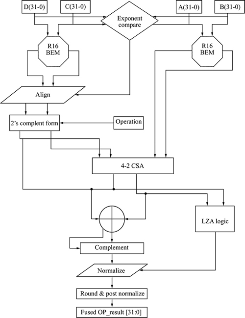
Fig. 2 Floating point fused dot product unit
The alignment block describes a pair of alignment shifter block. Each shifter block aids in arranging the output sum and carry of the ��C��D�� significand multiplication to the output sum and carry of the ��A*B�� significand multiplication. The alignment circuit determines the operation (addition or subtraction) to be performed between sum and carry of ��C��D�� and ��A*B�� as well. The difference between the exponents of the two operands of C&D serves as the support for this.
The normalization circuit helps in counting the number of leading zeros in the significand adder outcome and left-shifts the sum to have a leading one in the left-most digit. The LZA circuit has a pre-encoder and a leading zero detector (LZD) [11] as shown in Fig. 3. The normalization of the floating-point unit result is done with the use of LZA circuit, principally for subtraction operations in fused DP unit with massive offsets.
LZA [11]: pre-encode algorithm
For i=0 to n
Begin
 (6)
(6)
End
3.2 Proposed Radix-16 booth multiplier
The micro architecture block schematic of the significand multiplier is shown in Fig. 4. Actually, multiplication is the procedure of partial product generation and then addition of the generated partial products. There are many multiplication algorithms proposed in literature and these algorithms differ in generation of partial products and addition of partial products to evaluate the net result. Out of which booth��s encoding algorithm is the most popular multiplication algorithm. Also, the booth algorithm is effectively utilized for multiplication with modified Radix-r encoding method and is so called as modified Radix booth encoding multiplier. The most common encoding is Radix-4 booth encoding technique. In FFT Implementation with fused floating-point multiplier operation [11] Radix-8 booth encoding multiplier is used. This will reduce the number of partial product generation when compared to shift-add multiplier, array multiplier, and Radix-4 booth encoding multiplier architecture. Usually, in Radix-r booth��s algorithm the multiplier operand is often encoded into a Radix higher than 2 in order to reduce the number of partial products. Therefore, the higher the Radix-r the lesser will be the number of partial products generated. The encoding algorithm converts a series of successive 1��s into 0��s for the purpose of reducing the switching activity. Since r=2n each n+1 consecutive bits of the multiplier operand denotes the input to booth encoding circuit and the resultant from this circuit describes the suitable operation on the multiplicand operand that may be ��shift and invert��, ��invert��, ��equal to zero��, ��no operation�� and ��shift��, for example (-8A, -4A, -2A, -1A, 0, +1A, +2A, +4A, +8A) respectively. Thus, in this work a Radix-16 booth encoding multiplier algorithm circuit is proposed and it reduces the number of partial products generation by 75% compared to conventional multiplier, 50% compared to Radix-4 booth encoding multiplier, and 25% compared to Radix-8 booth encoding multiplier.
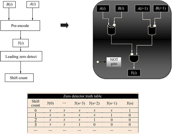
Fig. 3 LZA logic
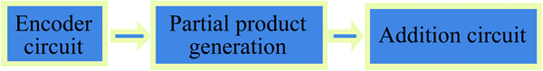
Fig. 4 Block schematic of proposed Radix-16 booth multiplier
In proposed Radix-16 booth encoding technique, a 24-bit multiplier operand (B0, B1, ��, B23)is sub divided into 6 groups with each group having 5-consecutive bits. These, groups are booth encoded as represented in second column of Table 1 and the same can be represented in encoded bits as in third column of Table 1, while the last column of Table 1 presents the operation to be performed over multiplier operand.
1) Proposed Radix-16 booth encoder circuit.
The Encoded bits are represented as a hardware circuit, as shown in Fig. 5. Thus, the proposed circuit is developed with respect to the relation between multiplicand input bits (A0, A1, ��, An) in column one and encoded bits in column three and is called as proposed Radix-16 booth encoder circuit. Also, the mathematical expression for the same is given by
 (7)
(7)
 (8)
(8)

 (9)
(9)

 (10)
(10)
 (11)
(11)
2) Proposed partial product generation circuit.
Since, the number of groups encoded is 6 for 24-bit multiplier, the number of partial products generated is 6. The partial product generation circuit utilizes last operation columns of Table 1. From the table it is clear that the operations performed by the partial product generation circuit are ��+1��A��, ��+2��A��, ��+4��A��, and��+8��A�� or ��-1��A��, ��-2��A��, ��-4��A��, and ��-8��A��, while these operations represent shifting left the multiplicand ��A�� by 0, 1, 2, and 3 respectively for positive operations and for negative operations the multiplicand ��A�� will be shifted left by 0, 1, 2, and 3 after performing 2��s complement of A, respectively. There is a probability that a partial product output will be 1 of the 8 different combinations +/- (A, 2A, 3A, 4A, 5A, 6A, 7A, and 8A) of encoder circuit driven operations. This is represented in the circuit Fig. 6.
Table 1 Proposed Radix-16 booth encoding table

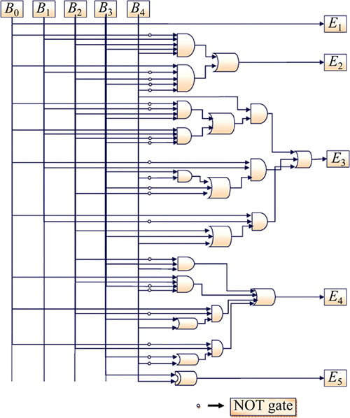
Fig. 5 Proposed Radix-16 booth encoder circuit
If the above partial product circuit is observed carefully, an 8:1 multiplexer with partial product select line logic circuit is interpreted. The 3-bit select line logic is designed such that gate logic circuit as shown in Fig. 7 utilizes the 4-output bits of the encoder circuit E2, E3, E4 and E5 to select 1 partial product from the 8 probable outputs. The mathematical model for the same is presented in Eqs. (12)-(14). The left shift operations are enabled based on the 4-output bits of the encoder circuit Fig. 6. Also, the positive and negative operations depend on the E1 bit. This maintains the synchronization between each operation of the partial product circuit. Again, the operation will be positive if E1 bit is 0 and it will be negative if E2 is 1, i.e., if E1 bit is 1 then 2��s complement of the multiplicand is first executed and then remainder will be shifted left with respect to the remaining encoder bits.
The mathematical representations of proposed partial product select line logic are
 (12)
(12)
 (13)
(13)
 (14)
(14)
3) Partial product addition circuit.
The selected 6 partial product need to be added to produce the desired result. The partial product addition is so designed that the ��0�� (zero) partial product generated is disabled form the addition circuit with the help of the enable logic for the 3: 8 decoder and 8:1 mux circuit. In Fig. 8, a 4-input OR gate is used to identify the low logic at active high enable signal (EN) of the decoder and mux. The 6 partial products are generated and stored in 49 bit partial product registers (PP0, PP1, PP2, PP3, PP4, and PP5). The orientation of these resultant partial product registers are sketched in Fig. 8. Now, these partial product registers are selected using a 3-bit up counter output as select line for 3:8 decoder and 8:1 mux. Again, if the EN (EN) input is 0, the decoder and mux will disable the partial product output to be decoded through to the adder unit and vice versa if EN input is 1. The enable logic reduces the switching activity and this is represented by a simple OR gate.

Fig. 6 Proposed partial product generator
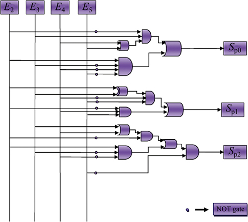
Fig. 7 Select line logic circuit
 .(15)
.(15)
3.3 Proposed Radix-4 DIT FFT
This section deals with a floating point fused Radix-4 FFT butterfly unit. This unit utilizes the IEEE-754 single precision format with Radix-16 booth encoding multiplier for mantissa multiplication. The Radix-4 FFT is an algorithm that constitutes the essential 4-point FFT computation element called butterfly unit. The Radix-4 FFT algorithm step-downs the amount of stages required for the implementation of FFT algorithm by executing more computations in the Radix-4 FFT butterfly unit. The principal merit of the Radix-4 FFT is that it attempts to lessen the number of complex multiplications by about 25% [17] in comparison to a same size Radix-2 FFT. Figure 9 illustrates the operation executed by Radix-4 decimation in time FFT butterfly unit. A Radix-4 FFT butterfly demands for eight complex additions and three complex multiplications for its operation.
The entire lines carry complex pairs of 32-bit IEEE-754 numbers and all operations are complex. A discrete realization of the parallel Radix-4 FFT butterfly unit demands 12 real multipliers and 6 real adders for the implementation of the 3 complex multipliers and 16 real adders for implementing the 8 complex adders, resulting in a total of 12 real multipliers and 22 real adders. Another fused realization is in need of 6 fused dot product units to implement the 3 complex multipliers and 8 fused add-subtract units to implement the 8 complex adders, resulting in a total of 6 fused DP units and 8 fused AS units. For the fused implementation, rounding and normalization takes place at the output of the fused dot product alone and once at each of the two layers of fused add-subtract units. This is illustrated in Fig. 10.
4 Implementation results and comparison
In this work a floating-point fused Radix-4 FFT butterfly unit is proposed using the IEEE-754 single-precision floating-point arithmetic format as shown in Fig. 11. The hardware utilization of the proposed fused butterfly design is compared to the conventional butterfly implemented with discrete floating-point multipliers and adders and to the fused butterfly design in Ref. [11]. The proposed fused butterfly unit is compared to the existing techniques for hardware utilization metrics such as; area and power. The proposed system is designed using Radix-16 booth encoding multiplier. The entire architecture is implemented in xilinx-ise and is coded in verilog language. For generating the hardware utilization report,the verilog code of the proposed architecture is synthesized and implemented using synthesis tool, while the power report is produced by using the xpower analyzer tool in xilinx-ise. Then, the simulation of the same is performed by developing a test bench for the proposed design.

Fig. 8 Partial product addition circuit
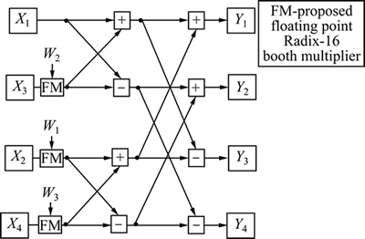
Fig. 9 Radix-4 DIT FFT butterfly unit
The implementation results presented for the above specifications are synthesized using vertex-4 FPGA device. To demonstrate the advantages of the proposed fused floating-point dot-product unit, the hardware utilization metrics for the following modules designed are analyzed:
1) Proposed Radix-16 booth encoding multiplier;
2) Proposed Radix-16 Fused Floating-Point Dot-Product Unit;
3) Proposed Radix-4 FFT Butterfly Unit.
The Proposed Radix-16 fused floating-point dot- product unit is shown in Fig. 2. Most of the sub-circuits of the proposed fused dot product unit are similar to the sub-circuits of the fused dot product unit [11]. The sub-circuits in proposed fused dot product differs from the one in Ref. [11] in the design of significand multiplier. The architecture shown in Figs. 5-8 contribute to the proposed significand multiplier. The Booth encoder shown in Table 1 reduce the number of partial products compared to the Radix-8 booth technique.

Fig. 10 Conventional complex arithmetic based butterfly unit
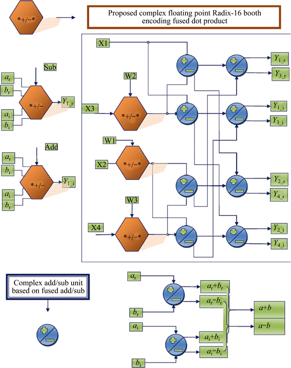
Fig. 11 Proposed complex arithmetic based Radix-4 DIT FFT butterfly unit
The partial product addition in Ref. [11] is executed by a Wallace carry save compression tree and a One-hot encoding is applied in organizing these partial products to nullify the overhead of executing full 2��s complement needed by Booth negative encoded digits. But, in this paper the 2��s complement is executed while the partial product is generated. The 2��s complement operation is executed only if the MSB of the encoded bits is high. And hence the complexity of executing the one hot encoding in partial product addition is eliminated. To produce the resultant value of significand multiplication, the partial products addition has to be aligned as shown in Fig. 12. And the another major contribution of the designed multiplier is that, it reduces the switching activities by disabling the zero encoded operation (0��A) for partial product addition as it will unnecessarily increase the switching activities.
The Radix-4 FFT butterfly unit utilizes the IEEE-754 single-precision floating-point multiplication and addition operations on the pairs of data. The proposed system is synthesized and implemented on the xc6vlx550tl-1Lff1759 FPGA device using Xilinx ISE tool.
5 Comparison of implementation results
5.1 Proposed Radix-16 booth encoding multiplier
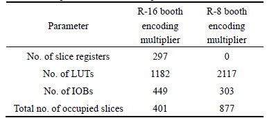
This circuit reduces the number of partial products generation by 75 % compared to conventional multiplier, and 25% compared to Radix-8 booth encoding multiplier. This results in 54.3% less space on the selected FPGA device. This fact is addressed in Table 2.
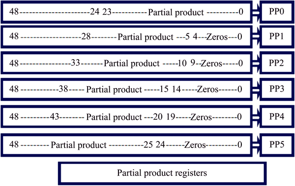
Fig. 12 Partial product registers
Table 2 Comparison of Booth multipliers
5.2 Proposed Radix-16 fused floating-point dot- product unit
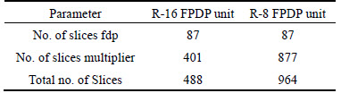
The proposed unit is superior to the technique presented in Ref. [11] since it occupies less space on the chosen device. This fact is addressed in the Table 3.
Table 3 Comparison of FPDP unit
5.3 Proposed Radix-4 FFT butterfly unit
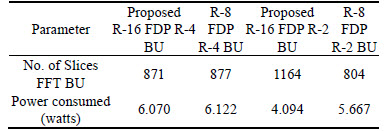
The proposed unit occupies less space compared and consumes less power to existing techniques presented in Ref. [11]. With the use of Radix-16 fused floating-point Dot-Product Unit, the area and power required will be reduced. This fact is addressed in Table 4.
6 Proposed enhancement
The analysis of the proposed model is effective in terms of area required, but consumes slightly less power than existing techniques as discussed in the abovesection. Therefore, in this section a further enhancement in the proposed model has been visualized. Enhancement in the proposed model is interpreted by utilizing the simple term reusability, the designed model in Fig. 11 can be realized as in Fig. 13 by examining Eqs. (16) to (31).
Table 4 Comparison of FFT architectures
x0��w0+x2��w2=A (16)
x0��w0+x2��w2=B (17)
x1��w1+x3��w3=C (18)
x1��w1+x3��w3=D (19)
Representing the above equations in complex multiplication and addition form;
(X0r+X2r)+(X0i+X2i)=Ar+Ai (20)
(X0r+X2r)+(-X0i-X2i)=Br+Bi (21)
(X1r+X3r)+(X1i+X3i)=Cr+Ci (22)
(X1r+X3r)+(-X1i-X3i)=Dr+Di (23)
where Xr (real value) and Xi (Imaginary value) are the fused dot product units which is constituted as
Xr=(xr��wr�Cxi��wi) and Xi=(xr��wi+xi��wr)
Finally,
Ar+Cr=Y0r (24)
Ar+Cr=Y1r (25)
Br+Dr=Y2r (26)
Br-Dr=Y3r (27)

Fig. 13 Detailed block representation of enhanced proposed model using reusability technique
Ai+Ci=Y0i (28)
Ai-Ci=Y1i (29)
Bi+Di=Y2i (30)
Bi-Di=Y3i (31)
Now, comparing Fig. 11 and Fig. 13, it is observed that the four FDP and four FAS modules can be considered as a part of reusability term. Form observation, it is clear that out of these 4-FDP and 4-FAS, a pair of 2-FDP and 2-FAS executes real and imaginary values of the complex multiplication and addition operations in FFT butterfly for a pair of input. Thus, these 2-FDP and 2-FAS modules of Radix-4 FFT butterfly unit can be utilized to generate the real and imaginary values for the 1st half of the output, while the remaining half of the output will be generated post execution of the 1st half of Radix-4 FFT butterfly unit. So the enhanced model will consume less power compared to the proposed model by utilizing the reusability technique. This is true, because the reusability technique allows only 2-FDP and 2-FAS modules out of 4-FDP and 4-FAS modules required to execute the operations of Radix-4 FFT butterfly unit.
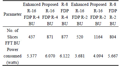
The enhanced model in Fig. 13 improves the results of the proposed model using the reusability technique. This consumes less space and power compared to existing techniques and as well as the proposed design in section 3-4. This fact is addressed in Table 5.
Table 5 Comparison of enhanced model with existing FFT architectures
7 Conclusions
1) The proposed Radix-16 Booth encoding multiplier based FDP unit for Radix-4 DIT FFT butterfly unit is synthesized and implemented on the xc6vlx550tl-1Lff1759 FPGA device using Xilinx ISE tool.
2) This system requires 12.16% less total power compared to the existing Radix-8 booth multiplier fused dot product based Radix-4 FFT butterfly unit (R-8 FDP based R-4 FFT BU). Similarly, R-16 FDP based R-2 FFT BU requires 5.11% less total power compared to the existing R-8 FDP based R-2 FFT BU.
3) On the other hand, the enhanced model with reusability technique benefits a power efficient butterfly unit.
4) The proposed enhanced R-16 FDP based R-4 FFT BU require 49.82% less hardware and reduced 11.42% of total power compared to the proposed R-16 FDP based R-4 FFT BU while, the proposed enhanced R-16 FDP based R-2 FFT BU requires 55.32% less space as well 10.08% reduced power consumption on the FPGA device equated to the proposed R-16 FDP based R-2 FFT BU.
5) Thus, from the comparison results it can be concluded that the proposed system is area and power efficient.
References
[1] IEEE Standard for Floating-Point Arithmetic, ANSI/IEEE Standard 754-2008 [S]. New York: IEEE, Inc., 2008.
[2] Montoya R K, Hokenek E, Runyon S L. Design of the IBM RISC system/6000 floating-point execution unit [J]. IBM Journal of Research & Development, 1990, 34: 59-70.
[3] Hokenek E, Montoya R K, Cook P W. Second-generation risc floating point with multiply-add fused [J]. IEEE J Solid-State Circuits, 1990, 25(5): 1207-1213.
[4] AL-ASHRAFY M, Salem A, Anis W. An efficient implementation of floating point multiplier [C]// Electronics, Communications and Photonics Conference (SIECPC). Saudi International, Ryadh: IEEE, 2011: 1-5.
[5] Quinnell E, Swartzlander Jr E E, Lemonds C. Bridge floating-point fused multiply-add design [J]. IEEE Transactions on Very Large Scale Integration (VLSI) Systems, 2008, 16(12): 1726-1730.
[6] Huang Li-bo, Ma Sheng, Shen Li, Wang Zhi-ying, Xiao Nong. Low-cost binary128 floating-point FMA unit design with SIMD support [J]. IEEE Transactions on Computers, 2012, 61(5): 745-751.
[7] MOTTAGHI-DASTJERDI M, AFZALI-KUSHA A, PEDRAM M. BZ-FAD: A low-power low-area multiplier based on shift-and-add Architecture [J]. IEEE Transactions on Very Large Scale Integration (VLSI) Systems, 2009, 17(2): 302-306.
[8] Yan Jin-tai, Chen Zhi-wei. Low-cost low-power bypassing-based multiplier design [C]// IEEE International Symposium on Circuits and Systems Paris: IEEE, 2010: 2338-2341.
[9] Kuo Ko-chi, Chou Chi-wen. Low power and high speed multiplier design with row bypassing and parallel architecture [J]. Microelectronics Journal, 2010, 10: 639-650.
[10] Prabhu A S, Elakya V. Design of modified low power booth multiplier [C]// International Conference on Computing, Communication and Applications, Dindigul: IEEE, 2012: 1-6.
[11] Galal S, Horowitz M. Energy-efficient floating-point unit design [J]. IEEE Transactions on Computers, 2011, 60(7): 913-922.
[12] Reddy B N K, Sekhar M C, Veeramachaneni S, Srinivas M B. A novel low power error detection logic for inexact leading zero anticipator in floating point units [C]// VLSI Design and 13th International Conference on Embedded Systems,Mumbai: IEEE, 2014: 128-132.
[13] SOHN J, SWARTZLANDER E E. Improved architectures for a floating-point fused dot product unit [C]// IEEE 21st Symposium on Computer, Arithmetic Proceeding ARITH��13, Anstin: IEEE, 2013: 41-48.
[14] Swartzlander E E, Saleh H H M. FFT Implementation with fused floating-point operations [J]. IEEE Transactions on Computers, 2012, 61(2): 284-288.
[15] Sohn Jong-wook, Swartzlander E E. Improved architectures for a fused floating-point add-subtract unit [J]. IEEE Transactions on Circuits and Systems��I: Regular Papers, 2012, 59(10): 2285-2291.
(Edited by DENG L��-xiang)
Received date: 2015-04-07; Accepted date: 2015-10-29
Corresponding author: Prabhu E; Tel: +91-9994205499; E-mail: e-prabhu@cb.amrita.edu

