
Annealing effects of Sn-Al and Sn-Cu nano thin films on mechanism of electromagnetic interference shielding
HUNG Fei-shuo1, HUNG Fei-yi2, CHIANG Che-ming1, LUI Truan-sheng3
1. Department of Architecture, National Cheng Kung University, Tainan, China;
2. Institute of Nanotechnology and Microsystems Engineering, Center for Micro/Nano Science and Technology,
National Cheng Kung University, Tainan, China;
3. Department of Materials Science and Engineering, National Cheng Kung University, Tainan, China
Received 21 October 2010; accepted 6 April 2011
Abstract: The sputtered Sn-Al and Sn-Cu thin films were used to investigate the effects of the crystallization mechanism and film thickness on the electromagnetic interference (EMI) characteristics. In addition, the annealed microstructure, electrical conductivities and EMI characteristics of the Sn-xAl films and the Sn-xCu films were compared. The results show that the electromagnetic interference (EMI) shielding of Sn-Al film was increased after annealing. For the Sn-Cu films with higher Cu mole concentration, the low frequency EMI shielding could not be improved. After annealing, the Sn-Cu thin film with lower Cu mole concentration possesses excellent EMI shielding at lower frequencies, but has an inverse tendency at higher frequencies.
Key words: electromagnetic interference (EMI); Sn-Al; Sn-Cu; thin film
1 Introduction
The effects of electromagnetic interference (EMI) are still being researched, and have even resulted in new legislation. Much research in epidemiology journals has shown that people who have been exposed to a high electromagnetic environment for a long duration become more susceptible to leukemia and brain tumors [1-2]. In addition, BLACKMAN et al [3] indicated that electromagnetic waves of over 60 Hz would cause damage and variations to the human body’s DNA structure. Relevant literature showed that people who have been exposed to a high electromagnetic environment for a long duration become more susceptible to diseases than normal people [4-6]. Therefore, how to use materials to improve the electromagnetic environment not only is a very important issue, but also conforms with the objective of environmental protection [4].
Electromagnetic interference is a new form of pollution discovered in recent years [7-10]. As of now, many laboratories are investigating the technology of EMI shielding. Some surface technologies possess better EMI shielding, including conductive films [11-17] and mixed conductive powders [18-21]. Problems such as wear, peeling, oxidation, hard-working and expensive cost have resulted in the applied capacity of applied materials to decrease. The elements Sn, Al and Cu not only possess EMI shielding efficiency, but also have acceptable costs [20] and can be used to make Sn-based thin films for EMI application. Because alloy thin films have better mechanical properties and a larger frequency range for EMI shielding, both Sn-xAl and Sn-xCu sputtering films were used not only to analyze the crystallized characteristics of the thin films, but also to investigate the effects of different additions of elements, thicknesses and annealed treatment of the EMI shielding to further understand the potential for use as an EMI shielding material.
2 Experimental
Sn-40Al and Sn-xCu (x=20% and 40%, mass fraction) sputtering thin films were used to perform the EMI shielding experiment. In the sputtering process (120 W), all films were sputtered onto a glass plate with dimensions of 2 cm×2 cm without any treatment. Four sputtered glasses made up an EMI specimen with dimensions of 4 cm×4 cm. The thickness of the Sn-40Al film was in the range of 380-760 nm. Some Sn-40Al films (380 nm) were annealed at 200 °C for 1 h in a vacuum, which are designated as 380 nm-H. As for the Sn-xCu specimens, the thickness of the Sn-20Cu film was 460 nm and that of the Sn-40Cu film was 710 nm. Some Sn-Cu films were annealed at 220 °C for 1 h in a vacuum, which are designated Sn-xCu-H. In order to understand the difference in characteristics of the films, the surface structures were examined using a scanning electron microscope (SEM: JEOL JSM-7001) to clarify the electromagnetic shield effect of the present Sn-based thin film systems.
The Elgal set 19A coaxial holder was used for electromagnetic interference shield testing. The range of scan frequency was from 300 kHz to 3 GHz, and its accuracy is ±10×10-6 (25±5 °C). A plane wave was used for vertical firing. The frequency range was controlled from 50 MHz to 3 GHz. Each datum was the average of at least 3-7 test results.
3 Results and discussion
According to our previous study on the EMI of Sn-xAl powders, high Al content coatings offered excellent low frequency EMI shielding. After the annealed treatment, the powders had higher electric conductivity able to enhance the EMI shielding. So, the present study selected the Sn-40Al sputtering film to investigate its EMI shielding. Figure 1 shows the appearance and the surface characteristics of the Sn-40Al sputtering films with 380 nm in thickness. Nano-grains are observed in the films using SEM and the surface characteristics of the other thin films are similar. Notably, the grain size in the present thin film was 22-46 nm and the other systems also possessed the identical microstructures.
When the film thickness was increased from 380 nm to 760 nm (Fig. 2(a)), there was an obvious promoting effect on the EMI shielding (Table 1). In fact, increasing the thickness of the film, not only raised its index of crystalline (IOC), but also enhanced the growth of nano-grains because of the longer sputtering duration. In order to avoid the effects of film thickness, grain size and IOC, the 380 nm-film was subjected to recrystallization (referred to as 380 nm-H) at 200 °C for 1 h in a vacuum, then cooled to room temperature with a cooling rate of 0.5 °C/min. EMI shieldings of the 380 nm-H-film and the 380 nm-film were compared. The EMI shielding of the 380 nm-H-film was higher than that of the 380 nm-film (Fig. 2(b) and Table 1).
In addition, the surface image of the 380 nm-H film showed no obvious difference compared with the 380 nm-film and the 380 nm-H film had a higher crystallization and lower resistivity. It is clear that the heat treatment (200 °C, 1 h) not only raised the electrical conductivity but also improved the high frequency EMI shielding. Figure 3 shows the XRD pattern of the Sn-40Al specimen. The results and a relevant report reveal that the solid solution limit of Al is low in Sn matrix, and the Sn-Al matrix not only affects the electric conductivity of the film, but also induces a variation in the EMI shielding [21]. We may say that the uniform distribution of Al-rich phases in Sn-Al thin film is able to enhance the EMI shielding.
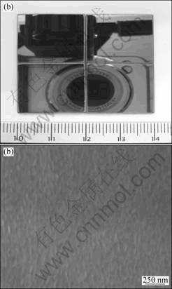
Fig. 1 Sn-40Al sputtering thin films (380 nm): (a) Appearance for four EMI specimens; (b) Surface characteristic
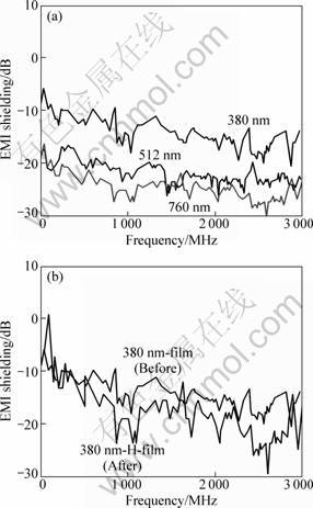
Fig. 2 EMI shielding of Sn-40Al sputtering thin films with different thicknesses (a) and before and after heat treatments (b)
Table 1 EMI shielding of Sn-40Al thin film at different frequencies
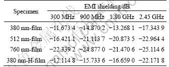

Fig. 3 XRD pattern of Sn-40Al film
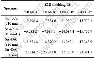
Since Sn-Cu specimens have higher electrical conductivity (1.08×10⁻⁴ W?cm for Sn-20Cu) and acceptable costs, the present study also used Sn-xCu to analyze the EMI mechanism and compared them with the Sn-40Al specimens. According to previous studies [25], Sn-based specimens with a high concentration of a second element had excellent EMI shielding in the range of scan frequency from 300 kHz to 3 GHz. So, the high Cu sputtered thin film (Sn-40Cu) was selected to investigate the EMI behavior. Figure 4 shows the EMI shielding of the Sn-40Cu (710 nm) and Sn-40Al (730 nm) thin films at a similar thickness, and the EMI shielding of the Sn-40Cu thin film was lower than that of the Sn-40Al thin film (Table 2). Notably, our previous data reveal that both the annealing treatment and higher film thickness not only increased the electric conductivity, but also enhanced the EMI shielding. But, after the annealing treatment, the EMI shielding of the Sn-40Cu film has a tendency to decrease. By comparing Fig. 4 with Fig. 5 and Table 2, it is different from the Sn-xAl films (annealed Sn-Al thin film was able to enhance the EMI shielding). Furthermore, the EMI of the annealed Sn-40Cu film with a greater thickness (710 nm) was still lower than that of the Sn-40Al film (un-annealed and with a smaller thickness of 380 nm). We can be fairly certain that the structure of the Sn-40Cu film had an obvious influence on the EMI shielding. It is very important to change the EMI shielding for annealed Sn-40Cu thin film.
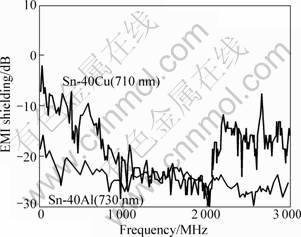
Fig. 4 EMI comparison of Sn-40Cu and Sn-40Al sputtering thin films with similar thickness

Fig. 5 EMI comparision of Sn-40Cu (annealed) and Sn-40Al (un-annealed) sputtering thin films
Table 2 EMI shielding of Sn-40Al and Sn-40Cu thin films
In Fig. 6, there are three phases (Cu6Sn5, Cu3Sn and β-Sn) in the Sn-40Cu film matrix, but no Sn/Al intermetallic compounds (IMCs) are observed in the Sn-Al thin film (Fig. 3). In other words, the volume ratio of Cu6Sn5, Cu3Sn and β-Sn phases is close to the EMI shielding. After annealing, the IMCs of the Sn-Cu thin film would increase, leading to a decrease in the electric conductivity (using four-point probe, Model 280 CI, Sn-40Cu: from 7.02×10⁻⁶ to 2.46×10⁻⁵ W?cm) and EMI shielding. So, this study avoided the effects of both IMCs and film thickness by decreasing the Cu content and measuring the EMI shielding before and after the annealing treatment. Under both constant Cu content (Sn-20Cu: lower IMCs) and thickness (Fig. 7), the annealed Sn-20Cu film showed the greater EMI shielding at higher frequencies, but an inverse tendency was found at lower frequencies.
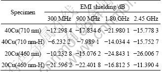
The experiment result was that the annealing treatment made a greater contribution for low Cu content specimens (Table 3). According to our previous studies on Sn-based [21], the reason for this is not hard to see: 1) β-Sn phase is the main EMI shielding mechanism; 2) the complex compounds after annealing possess higher thermal stabilization to promote the EMI shielding. The present results indicate that increasing thickness or having an annealing improved the EMI shielding of Sn-40Al thin film (Fig. 8(a)). Take Sn-xCu thin films with 20%Cu to 40%Cu for example, the annealing

Fig. 6 XRD patter of Sn-40Cu thin film
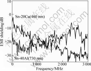
Fig. 7 Effect of frequency on EMI annealed Sn-20Cu thin films

Fig. 8 EMI shielding characteristics: (a) Sn-40Al thin films; (b, c) Sn-xCu thin films
Table 3 EMI shielding of Sn-xCu thin film
4 Conclusions
1) For the Sn-Al films, increasing the film thickness the electric conductivity and improved the EMI shielding. As for the Sn-Cu films, due to the large number of IMCs and lower content of β-Sn, the higher frequency EMI shielding of the annealed Sn-Cu thin films deteriorated.
2) The Sn-Al films had Sn-rich phases and Al-rich phases in matrix, which were able to promote the EMI shielding. Their annealing treatment not only provided higher electric conductivity but also increased the high frequency EMI shielding.
Acknowledgements
The authors are grateful to the Center for Micro/ Nano Science and Technology, National Cheng Kung University (NCKU Project of Promoting Academic Excellence & Developing World Class Research Center: D97-2700) and NSC 98-2221-E-006-068; NSC 98-2622-E-006-024-CC3 for the financial support.
References
[1] POLK C, POSTOW E. Hand book of electromagnetic fields [M]. 2nd ed. Florida: CRC Press Inc, 1996: 212-213.
[2] BLACKMAN C F, BLANCHARD J P, BENANE S G, HOUSE D E, FASEB J. The ion parametric resonance modelpredicts magnetic field parameters that affect nerve cells [J]. FASEB Journal, 1995, 9: 547-551.
[3] BLACKMAN C F, BENANE S G, RABINOWITJ J R, HOUSE D E, JOINES W T. Action of 50 Hz magnetic fields on neurite outgrowth in pheochromocytoma cells [J]. Bioelectromagnetics, 1985, 6: 327-338.
[4] CHIANG C M, LAI C M. A study on the comprehensive indicator of indoor environment assessment for occupants’ health in Taiwan [J]. Building and Environment, 2001, 37: 387-392.
[5] MCLEOD B R, LIBOFF A R. Low frequency magnetic interference in high-rise buildings [J]. Bioelectromagnetics, 1986, 7: 177-189.
[6] FECHTING M, AHLBOM A. Magnetic fields and cancer in children residing near Swedish high voltage power lines [J]. Am J of Epidemiol, 1993, 138: 467-481.
[7] BURNETT J, DU Y. Low frequency magnetic interference in high-rise buildings [C]//Seventh International IBPSA Conference, Building Simulation, vol. 7, 2001: 327-333.
[8] GRESHAM R M. Plating and Surface finishing [J]. J Applied Surface Science, 1998, 13: 63-69.
[9] TENFORDE T S. Interaction of ELF magnetic fields with living systems [M]//POLK C, POSTOW E. Handbook of Biological Effects of Electromagnetic Fields. 2nd ed. Boca Raton, Florida: CRC Press, 1996.
[10] TENFORDE T S, KAUNE W T. Interaction of extremely low frequency electric and magnetic fields with human [J]. Health Phys, 1987, 53: 585-606.
[11] WERTHEIMER N, LEEPER E. Electrical wiring configurations and childhood cancer [J]. Am J Epidemiol, 1979, 109: 273-284.
[12] MERCHANT C J, RENEW D C, SWANSON J. Exposures to power frequency magnetic field in the home [J]. Journal of Radiological Protection, 1994, 14(1): 77-87.
[13] SALISBURY W W. Absorbent body for electromagnetic waves: U. S. 259994410 [P]. 1952.
[14] ZHADIN M N, FESONKO E E. Magnetic fields and cancer in children residing near Swedish high voltage power lines [J]. Biomed Sci, 1990, 1: 245-250.
[15] WHITE G E. Liquid crystalline polymer and multilayer polymer-based passive signal processing components for wireless multi-band applications: U. S. 20070085108 [P]. 2007.
[16] BRUCKNER-LEA C, DURNEY C H, JANNTA J, RAPPAPRT C, KAMINSKI M. Causes and indicators of housing quality [J]. Social Indicators Research, 1978, 5(2): 195-210.
[17] GRESHAM R M. EMI/RFI shielding of plastics [J]. Plating and Surface Finishing, 1988, 2: 63-69.
[18] WENDEROTH K, PETERMANN J. Synergism on electro-magnetic interference (EMI) shielding in metal and ferroelectric-particle filled polymers [J]. Polymer Composites, 1989, 10(1): 52-56.
[19] SALISBURY W. Absorbent body for electromagnetic waves: U. S. 2599944 [P]. 1952-06-10.
[20] FANTE R L, MCCORMACK M T. Reflection properties of the Salisbury screen [J]. IEEE Trans Antenna Propagation, 1998, 36: 1443-1454.
[21] LIU J C, HO S S, BOR S S. Techebyshev approximation method for Salisbury screen design [J]. IEEE Proceeding H, 1993, 140(5): 414-416.
热处理效应对Sn-Al与Sn-Ca纳米薄膜的电磁屏蔽机制
洪飞硕1,洪飞义2,江哲铭1,吕传盛2
1. 国立成功大学 建筑学系,台南;
2. 国立成功大学 纳米科技微工程研究所,台南;
3. 国立成功大学 材料科学与工程学系,台南
摘 要:利用溅镀Sn-Al纳米薄膜和Sn-Cu纳米薄膜讨论结晶机制与膜厚对电磁波屏蔽特性的影响,比较了Sn-Al和Sn-Cu薄膜的高温显微组织、导电性与电磁波屏蔽性能。结果表明,高温处理提高了Sn-Al纳米薄膜的电磁波屏蔽性。在低频条件下,高Cu摩尔浓度的Sn-Cu纳米薄膜不能有效改善电磁波屏蔽性;高温处理后,低Cu摩浓度的Sn-Cu纳米薄膜能提高低频的电磁波屏蔽性,而高频下的电磁波屏蔽性则呈相反趋势。
关键词:电磁波屏蔽;Sn-Al;Sn-Cu;薄膜
(Edited by LI Xiang-qun)
Corresponding author: HUNG Fei-yi; E-mail: N7895122@nckualumni.org.tw
DOI: 10.1016/S1003-6326(11)60966-7