Article ID: 1003-6326(2005)02-0414-05
Influences of post-annealing and internal stress on magnetoresistance properties of Ni80Fe20 films
GAO Yan-qing(������), WU Ping(�� ƽ), CAI En-jing(�̶���),
QIU Hong(�� ��), WANG Feng-ping(����ƽ),
PAN Li-qing(������), TIAN Yue(�� Ծ)
(Department of Physics, University of Science and Technology Beijing, Beijing 100083, China)
Abstract: Ni80Fe20 films with thickness about 54nm were deposited on K9 glass and thermally oxidized silicon substrates at ambient temperature by electron beam evaporation with deposition rate about 1.8nm/min. The as-deposited films were annealed at 350, 450 and 570��respectively for 1h. After annealing at 570��, the anisotropic magnetoresistance ratio(RAM) of the films is greatly improved. It increases to 3%-3.5% nearly about three times of that of the as-deposited films. The grain size increases with the annealing temperature and the [111] crystal orientation is obviously enhanced after annealing at temperature above 450��. The internal stress in the films deposited on K9 glass is compressive and the resistance measurement shows that RM�� is larger than RM�� in these films. However, in the films deposited at the same conditions but on oxidized silicon substrates, the internal stress is tensile and RM�� is larger than RM��. The differences of RM�� and RM�� in two series of specimens are discussed.
Key words: Ni80Fe20 film; annealing; internal stress; anisotropic magnetoresistance CLC number: O484.4
Document code: A
1 INTRODUCTION
NiFe films have been widely investigated because of their excellent magnetic properties such as high magnetoresistance, low coercivity and high magnetic permeability[1]. NiFe as an important magnetic material has been applied in magnetic and electronic devices such as magnetic recording heads, magnetoresistive sensors[2-4]. There are many factors which influence the anisotropic magnetoresistance ratio(RAM) of NiFe films. In previous works, it was found that RAM of NiFe films has much relation to film thickness, substrate temperature[2], deposition methods [5], ect. The appropriate seed layers can yield high RAM and good magnetic properties[6-8]. Lee et al found that a thin NiFeCr seed layer can yield high RAM of 3.2% for thin NiFe films[9]. Annealing treatment can also improve RAM and magnetic properties of NiFe films markedly [3, 10]. Because an internal stress in the thin films affects the reliability and the magnetic properties, the stress and its evolution in NiFe films attract much attention[11-13]. Some researchers studied the internal stresses in permalloy films prepared with different deposition parameters and found that the stress can be reduced by the appropriate combination of deposition parameters[14]. Bruckner et al investigated the internal stress origin and evolution in NiFe thin films during annealing[15]. However, the influence of the internal stress on the magnetoresistance properties is not very clear. The aim of the present work is to study the influences of annealing temperature and internal stress in the films on the magnetoresistance properties of Ni80Fe20 films.
2 EXPERIMENTAL
Ni80Fe20 films with thickness about 54nm were deposited on K9 glass(about 2mm thick) and thermally oxidized silicon substrates at ambient temperature by electron beam evaporation with deposition rate about 1.8nm/min. The base pressure was lower than 6��10-4Pa. The size of the specimens was about 12mm long and 5mm wide. The as-deposited films were respectively annealed at 350, 450 and 570�� in a vacuum lower than 3��10-3Pa for 1h. The anisotropic magnetoresistance ratios of the films were measured using a four-point probe technique. The microstructure and morphology of the films were determined by X-ray diffraction(XRD) and atomic force microscopy(AFM). Auger electron spectroscopy(AES) measurements were carried out to analyse the composition of the NiFe films.
3 RESULTS AND DISCUSSION
3.1 Magnetoresistance
The saturation resistances measured by applying a magnetic field parallel and perpendicular to the sensing current are denoted as R�� and R�� respectively. The anisotropic magnetoresistance ratio RAM can be defined as[16]

The resistances measured with and without magnetic field are denoted as R(H) and R(0). Then magnetoresistance ratio RM is given by

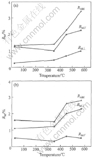
The values of parallel magnetoresistance ratio RM��(the sensing current parallel to the magnetic field), perpendicular magnetoresistance ratio RM��(the sensing current perpendicular to the magnetic field) and RAM are shown as a function of annealing temperature in Fig.1. For the films deposited on K9 glass substrates, as-deposited and annealed, RM�� is larger than RM��, while for the films deposited on thermally oxidized silicon substrates RM�� is larger than RM��.

Fig.1 RM��, RM�� and RAM for as-deposited and post-annealed NiFe films deposited on
K9 glass substrates(a) and thermally oxidized silicon substrates(b)
It can also be seen from Fig.1 that the values of RAM of the films deposited on the two different kinds of substrates increase with annealing temperature increasing. After annealing at a temperature below 350��, RAM almost does not change compared with that of the as-deposited films. But after annealing at 570��, RAM is greatly improved. It increases to 3%-3.5% nearly about three times that of the as-deposited films. Furthermore, the RAM sensitivity for magnetic field increases from about 7.5��10-4%/(A��m-1) for the as-deposited films to about 2.4��10-3%/(A��m-1) for 570��-annealed films. It can be seen that high temperature annealing treatment can significantly improve RAM and its magnetic sensitivity of the films.
3.2 Microstructure and internal stress
Fig.2 shows the XRD patterns of the Ni80Fe20 films. From Fig.2 it can be seen that the [111] crystal orientation is obviously enhanced after annealing at temperature above 450�� and a weak peak of (200) is observed. According to the results of the magnetoresistance measurements and the XRD patterns, it can be considered that RAM of the NiFe films increases with the enhancement of the [111] texture. The grain size of the films was estimated from the full width at half maximum of XRD peaks of (111). It is found that the grain size increases from about 3nm for the as-deposited films to about 6nm for 570��-annealed films. In conclusion, 570�� post-annealing treatment can greatly improve the crystalline quality and the grain growth of the films.

Fig.2 XRD patterns of NiFe films deposited on K9 glass substrates(a) and thermally oxidized
silicon substrates(b)
The internal stress in the as-deposited and post annealed films can be analyzed from the data of XRD patterns. Under the assumption that the film remains elastic, the stress �� in the film can be calculated by the equation[15]

where E and �� are elastic modulus and Poisson��s ratio of the film respectively; L is the lattice constant of the film which can be calculated by the data of XRD; L0 is the lattice constant of NiFe bulk. For Ni80Fe20, E=210GPa. Also ��=0.31 for Ni[15] was used as an estimate of �� for Ni80Fe20. The calculated stress in the films are listed in Table 1. ��>0 indicates a tensile stress induced in the film while �ҡ�0 represents a compressive stress induced in the film.
Table 1 Values of internal stress �� for as-deposited and post-annealed NiFe films
deposited on K9 glass substrates and thermally oxidized silicon substrates

From Table 1, it can be seen that the variations of �� in two series of films with the annealing temperature are different. In the films grown on K9 glass, a compressive stress exists while in the films grown on thermally oxidized silicon substrates a tensile stress exists.
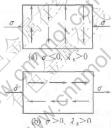
The internal stress in the films may cause changes in the magnetic properties of the films. When ��s��>0(��s: spontaneous magnetostrictive coefficient), the spontaneous magnetic moment, M, rotates to the stress direction; when ��s�ҡ�0, M tends to be perpendicular to the stress direction[16].
For Ni80Fe20, ��s>0[16]. The influence of stress �� on the spontaneous magnetic moment direction in two series of specimens are shown in Fig.3. For the films deposited on K9 glass ��s�ҡ�0 and M tends to be perpendicular to the stress direction while for the films deposited on thermally oxidized silicon substrates ��s��>0 and M tends to be parallel to the stress direction.

Fig.3 Influence of stress �� on spontaneous magnetic moment direction in NiFe films
deposited on K9 glass substrates(a) and thermally oxidized silicon substrates(b)
Dependence of anisotropic resistivity on the angle between sensing current and magnetic moment, ��, can be expressed as[16]
��(��)=����+(����-����)cos2��(4)
where ���� and ���� are the saturation resistivities when the applied magnetic field parallel and perpendicular to the sensing current, respectively.
For the films deposited on thermally oxidized silicon substrates, ��s��>0 and M tends to be parallel to the stress direction. If a sensing current is applied parallel to the stress direction and a magnetic field is applied parallel to the sensing current, �� will change slightly or almost not change with the increase of the applied magnetic field resulting in a small value of RM��. While if the magnetic field is applied perpendicular to the sensing current, �� will change from ��/2 to 0 with the increase of the applied magnetic field and the value of RM�� will be relatively large. Therefore RM��is larger than RM�� in these films. For the films deposited on K9 glass, because M tends to be perpendicular to the stress direction, the situation is just contrary to that of the films deposited on thermally oxidized silicon substrates. According to the above discussion, the different initial spontaneous magnetization direction causes RM��>RM�� for the films grown on K9 glass and RM����RM�� for the films grown on thermally oxidized silicon substrate. And the different initial spontaneous magnetization direction is due to the different internal stress states in the two series of films.
3.3 Morphology
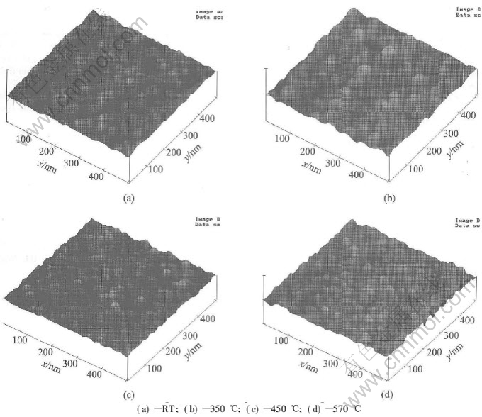
For the films deposited on K9 glass substrates and thermally oxidized silicon substrates annealed at the same temperatures the AFM microphotographs of film surface are similar. Fig.4 shows the AFM microphotographs of the films deposited on K9 glass substrates. As seen in Fig.4, the grain size increases after annealing at 350�� while almost does not change after annealing at 450�� and 570��. AES analyses show that for the specimen annealed at 570��, the contents of O and C at surface are much higher than that of the as-deposited one, however no obvious differences are shown in the contents of O, C, Ni and Fe in the film bulk for as-deposited and 570�� annealed films. Therefore the surface morphology of the specimens annealed at high temperature shown by AFM may be the oxidized surface layer. The XRD patterns verify that the grain size increases with annealing temperature increasing.

Fig.4 AFM microphotographs of as-deposited and
post-annealing NiFe films deposited on K9 glass substrates
4 CONCLUSIONS
Ni80Fe20 films with thickness about 54nm were annealed at 350, 450 and 570�� for 1h respectively. It is found that after 570�� post-annealing the RAM of the Ni80Fe20 films can be greatly improved to 3%-3.5%. The [111] crystal orientation is obviously enhanced after annealing at temperature above 450��. The internal stress in the films deposited on K9 glass is compressive and RM�� is larger than RM��. However in the films deposited at the same condition but on oxidized silicon substrates the stress is tensile and RM�� is larger than RM��. The difference of RM�� and RM�� in two series of specimens is due to the difference in the internal stress.
REFERENCES
[1]Yang J, Barna A, Makihara K, et al. Growth structure and properties of Fe rich Fe-Ni alloy films deposited on MgO(001) by d.c-biased plasma-sputtering [J]. Thin Solid Films, 1999, 347: 85-90.
[2]Miyazaki T, Ajima T, Sato F. Dependence of magnetoresistance on thickness and substrate temperature for 82Ni-Fe alloy film [J]. Journal of Magnetism and Magnetic Materials, 1989, 81: 86-90.
[3]Funaki H, Okamoto S, Kitakami O, et al. Improvement in magnetoresistance of very thin permalloy films by post-annealing [J]. Jpn J Appl Phy, 1994, 33(9B): L1304-L1306.
[4]Hans H, Gunther S, Johann H. High-performance magnetoresistive sensors [J]. Sensors and Actuators, 2000, 81: 27-31.
[5]Yukimasa Y, Satoshi O, Osamu K, et al. Crystal structure and magnetoresistance of Fe10Ni90 films deposited by sputter-beam method [J]. Jpn J Appl Phy, 1993, 32(9A): L1222-L1224.
[6]Gong H, Litvinov D, Klemmer T J, et al. Seed layer effects on the magnetoresistive properties of NiFe films [J]. IEEE Transactions on Magnetics, 2000, 36(5): 2963-2965.
[7]Lee W Y, Toney M F, Tameerug P, et al. High magnetoresistance permalloy films deposited on a thin NiFeCr or NiCr underlayer [J]. J Appl Phy, 2000, 87(9): 6992-6994.
[8]Jerome R, Valet T, Galtier P. Correlation between magnetic and structural properties of Ni80Fe20 sputtered thin films deposited on Cr and Ta buffer layers [J]. IEEE Transactions on Magnetics, 1994, 30(6): 4878-4880.
[9]Lee W Y, Toney M F, Mauri D. High magnetoresistance in sputtered permalloy thin films through growth on seed layers of (Ni0.81Fe0.19)1-xCrx [J]. IEEE Transactions on Magnetics, 2000, 36(1): 381-385.
[10]Krongelb S, Gangulee A, Das G. Annealing of thin magnetoresistive permalloy films [J]. IEEE Transactions on Magnetics, 1973, 9(3): 568-570.
[11]Jen S U, Huang K P, Kuan Y C. The effect of substrate temperature on stress, magnetic anisotropy and magneto-resistance of Co-Ni films [J]. Journal of Materials Science Letters, 1999, 18: 537-539.
[12]Spaepen F. Interfaces and stresses in thin films [J]. Acta Materialia, 2000, 48: 31-42.
[13]Pauleau Y. Generation and evolution of residual stresses in physical vapour-deposited thin films [J]. Vacuum, 2001, 61: 175-181.
[14]England C D, Falco C M. X-ray diffraction determination of stress in magnetron-sputtered permalloy films [J]. J Appl Phy, 1988, 63(8): 3227-3229.
[15]Brucker W, Thomas J, Schneider C M. Evolution of stress and microstructure in NiFe(20 wt.%) thin films during annealing [J]. Thin Solid Films, 2001, 385: 225-229.
[16]Mcguire T R, Potter R I. Anisotropic magnetoresistance in ferromagnetic 3d alloys [J]. IEEE Transactions on Magnetics, 1975, 11(4): 1018-1038.
Foundation item: Project(20040600290) supported by the Scientific Research Development Foundation of University of Science and Technology Beijing
Received date: 2004-12-16; Accepted date: 2005-01-18
Correspondence: WU Ping; Tel: + 86-10-62333786; E-mail: pingwu@sas.ustb.edu.cn
(Edited by HE Xue-feng)