Fabrication of integrated resistors in printed circuit boards
来源期刊:中南大学学报(英文版)2011年第3期
论文作者:王守国 陈清远
文章页码:739 - 743
Key words:integrated resistors; lamination method; printed circuit boards; integrated passive technology
Abstract: In order to utilize integrated passive technology in printed circuit boards (PCBs), manufacturing processing for integrated resistors by lamination method was investigated. Integrated resistors fabricated from Ohmega technologies in the experiment were 1 408 pieces per panel with four different patterns A, B, C and D and four resistance values of 25, 50, 75 and 100 Ω. Six panel per batch and four batches were performed totally. The testing was done for 960 pieces of integrated resistors randomly selected with the same size. The value distribution ranges and the relative standard deviation (RSD) show that the scatter degree of the resistance decreases with the resistor size increasing and/or with the resistance increasing. Patterns D with resistance of 75 and 100 Ω for four patterns have the resistance value variances less than 10%. Patterns C and D with resistance of 100 Ω have the manufacturing tolerance less than 10%. The process capabilities are from about 0.6 to 1.6 for the designed testing patterns, which shows that the integrated resistors fabricated have the potential to be used in multilayer PCBs in the future.
J. Cent. South Univ. Technol. (2011) 18: 739-743
DOI: 10.1007/s11771-011-0756-9![]()
WANG Shou-guo(王守国)1, CHAN Ching-yuen(陈清远)2
1. School of Information Science and Technology, Northwest University, Xi’an 710127, China;
2. Department of Industrial and Systems Engineering, The Hong Kong Polytechnic University, Hong Kong, China
? Central South University Press and Springer-Verlag Berlin Heidelberg 2011
Abstract: In order to utilize integrated passive technology in printed circuit boards (PCBs), manufacturing processing for integrated resistors by lamination method was investigated. Integrated resistors fabricated from Ohmega technologies in the experiment were 1 408 pieces per panel with four different patterns A, B, C and D and four resistance values of 25, 50, 75 and 100 Ω. Six panel per batch and four batches were performed totally. The testing was done for 960 pieces of integrated resistors randomly selected with the same size. The value distribution ranges and the relative standard deviation (RSD) show that the scatter degree of the resistance decreases with the resistor size increasing and/or with the resistance increasing. Patterns D with resistance of 75 and 100 Ω for four patterns have the resistance value variances less than 10%. Patterns C and D with resistance of 100 Ω have the manufacturing tolerance less than 10%. The process capabilities are from about 0.6 to 1.6 for the designed testing patterns, which shows that the integrated resistors fabricated have the potential to be used in multilayer PCBs in the future.
Key words: integrated resistors; lamination method; printed circuit boards; integrated passive technology
1 Introduction
Resistors, capacitors, inductors, and their combinations are categorized as passive components, which do not introduce gain or do not have directional functions. Conventionally, there are two application techniques for passive components: the surface mount technology (SMT) and the packaging through hole (PTH) technology. SMT devices are taking place of the PTH devices gradually from their easy use in PCBs. Today, SMT devices are the most commonly used discrete passive components. However, higher frequency for the circuit, smaller size demanding for the equipments, and the better reliability requirement for the PCBs need new technologies [1]. Therefore, the integrated passive technology has been developed to meet these requirements [2]. Integrated passive technology is a process of embedding passive devices into PCBs. The implementation of integrated passive devices can further miniaturize the physical size of a PCB, which will be important to the electronic appliances, such as the cellular phones, personal data assistants, and camcorders, because the passive devices usually contribute 80% or more of the total number of components and consume up to 40% of the surface area of a PCB [3]. By burying resistors and capacitors in the inner layers of multiplayer PCBs, passive components can be placed directly below active devices like integrated circuits (ICs). The reduction of solder joints can enhance the PCBs reliability because they are the main failure modes [4]. The achievement of shorter distance between the integrated passives and ICs reduces the parasitic effects associating with the current SMT devices, resulting in better signal transmission, less cross talk, lower loss and lower noise, which are attractive characteristics especially in high frequency applications. Therefore, the method of integrated capacitors has been believed as an effective means of reducing noise in the PCB power buses [5].
Currently, some fabrication methods of integrated passives in the PCBs are under investigation by several well-known research groups such as the National Center for Manufacturing Science (NCMS), 3M, Dupont, and Ohmega [6-7]. Their methods include the low temperature co-fired ceramics (LTCC) [8], lamination approach [9], thin film deposition technique [10] and plating method [11]. The material and characteristics of various embedded passive techniques are different as well as their fabrication methods. Each has limitation in the resistance range, temperature coefficient and value tolerance. The designers will no longer look at the PCB as an intricate connections provider, but instead will see it as a sophisticated, integral part of a system. As a new solution for PCBs design, there are many research works waiting to be done before the application of the embedded passives maturely.
In this work, the fabrication processing for embedded resistors by lamination method was investigated. Four different testing patterns with four different resistance values were designed. The resistance value distribution range for every resistor size, relative standard deviation (RSD), product value variances, manufacturing tolerance from design value, and process control ability for manufacturing process were given and discussed in detail.
2 Design of layout
The initial board for integrated resistor in the experiment was nickel phosphorus (NiP) covered with copper foil from Ohmega technologies, so the resistor material was NiP layer. A testing pattern with four different size values was designed, as shown in Fig.1. The resistor material was located in the center with different sizes. According to four different ratios of the length to the width for the resistors, four resistance values were gotten in a pattern. At the end of the conductor trace, there were eight pieces of rectangle pads which were designed for testing the resistance value with a conductor analysis Testing (CAT) equipment.
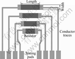
Fig.1 Testing pattern of integrated resistors
In order to investigate the size effects for the embedded resistors and directional manufacturing ability for the fabrication process, four different patterns A, B, C and D were designed with the length and width listed in Table 1. The standard sheet resistivities for Ohmegaply were 10, 25, 50, 100, 250 Ω/□ and 50 Ω/□ was used here. There were 16 different size resistors in a testing module with four resistance values of 25, 50, 75 and 100 Ω in total.
Each module was then put into a 450 mm×600 mm laminate core panel for fabrication in the PCBs processing line. The whole panel layout of the testing panel was designed by computer aided design (CAD) software, as shown in Fig.2. The design patterns were orientated in four directions within a module, which were marked by A, B, C and D in Fig.2. The integrated resistor layouts were plotted with laser plotter on the photo masks which were used for exposure in integrated resistor fabrication.
Table 1 Size of pattern in module
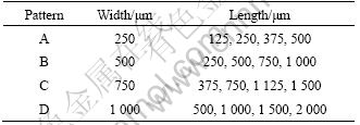
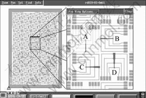
Fig.2 Computer aided design (CAD) software interface for artwork design
As there were totally 88 modules in a panel and each module had 16 different size resistors with 4 different resistance values, the total number of integrated resistors fabricated per panel would be 1 408 pieces.
3 Fabrications process
Manufacture of integrated passive devices by lamination method is performed essentially by shaping and etching resistor material layers and electrode layers with photolithography process. At present, it seems a potentially commercial way for fabricating integrated passive devices. The construction used by lamination method is a sandwiching structure which has four layers for a board with integrated resistors, including two layers of the copper foils (top and bottom), a film resistor layer NiP, and a dielectric layer (epoxy glass cloth). The values of resistors are determined by their shapes and are obtained by etching method. Although there is still the NiP layer beneath the copper layer, a current will go through along the conductor trace (copper layer) and the NiP resistor region in the least resistance path way. Similarly, the shape of electrodes and the trace line are also produced by etching.
Six panels as a batch were scrubbed on pumice scrubbing machine with band width of 10 mm, pumice content of 25%, water washing of 18 s, conveyor speed of 2 m/min, rinse pressure of 2 MPa and dry temperature of 90 °C. The 450 mm-wide photoresist layers were applied to cover the panels under the conditions of hot rolling temperature of 90 °C, tension plate pressure of 0.4 MPa, tension plate temperature of 60 °C, and laminating speed of 2 m/min. The panels were finished to exposure under 0.1 MPa vacuum and get 8 grade in Stouffer 21-step sensitivity guide. The panels were exposured at a parallel light exposure machine with pattern side facing the bottom light. After normal exposure, the panels were developed with K2CO3 content of 1.0%, developing pressure of 0.18 MPa, developing speed of 2.5 m/min, developing temperature of 30 °C, water rinse pressure of 0.18 MPa and drying temperature of 90 °C. Then, they were etched by 0.13 g/cm3 CuSO4 and 0.18 g/cm3 HCl, under pH value of 8.2, etching temperature of 50 °C and etching pressure of 0.15 MPa for the copper layer and followed by 0.25 g/cm3 CuSO4・5H2O and 0.5% H2SO4 for the NiP layer. The unprotected copper with NiP layer was etched away together and almost no undercuts of resistance materials were found. In the first photolithography process, the copper circuit areas and the NiP resistor regions with the testing patterns (the width of integrated resistors) were formed. And then, the photoresist films were stripped at a stripping pressure of 0.15 MPa, a stripping temperature of 50 °C, water rinse pressure of 0.2 MPa, and a drying temperature of 60 °C. The panels were cleaned and dried. With the same conditions as mentioned above, the second photolithography with the photoresist layer application, exposure, development, and etching was done in turn. The copper on top of the NiP resistor area was etched away and the resistor materials were left, so the lengths for integrated resistors were determined. Now, copper tracks were left on the top of NiP layer linked by the NiP resistor areas. After being cleaned and dried, the products with integrated resistors were gotten. There were four batches of the testing panels fabricated in the experiment.
A concise fabrication processing for integrated resistors in the experiment is shown below.
1) Boards were scrubbed with pumice scrubbing machine;
2) Boards were covered by photoresist layers;
3) Boards were lithographed firstly with the exposure, development, and etching in turn;
4) The photoresist layers were stripped;
5) Boards were covered by photoresist layers and lithographed secondly;
6) Boards were cleaned and dried.
4 Measurements and discussion
Nine hundred and sixty pieces of integrated resistors with the same size are chosen randomly from four batches, with six panels per batch and forty pieces per panel. According to the four different patterns A, B, C and D and the four design resistances 25, 50, 75, and 100 Ω, the minimum and the maximum resistances for every resistor size are tested, as shown in Fig.3. It can be seen that the scattering degree of the resistance values decreases with the resistors size increasing and/or with the resistance value increasing.
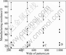
Fig.3 Resistance tested for every integrated resistor size
The numerical values for great quantity integrated resistors show a normal distribution. The scattering degree of the resistance data will be described by the standard deviation σ, which can be gotten in a statistical method. With the mean resistance value Rmean, the relative standard deviation (RSD) for the integrated resistors can be defined by
σR=σ/Rmean (1)
It is a unified principle to judge the manufacturing quality consistence for different patterns, as shown in Fig.4. The RSD decreasing from pattern A to D shows that the consistency becomes better with increasing the size of the integrated resistor in this experiment. This tendency is also similar for the resistance values from 25 to 100 Ω, as shown in Fig.3.
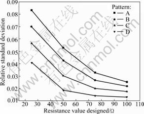
Fig.4 Relativity standard deviations for test patterns
The resistance value ranges of the integrated resistors give expression to the manufacturing yield. The variance of the resistance values for resistors can be calculated by
Y=(Rmax-Rmin)/2Rmean (2)
where Rmax and Rmin are the maximum and minimum resistances of integrated resistor. Figure 5 gives the variance Y for every pattern in different resistance values. If 10% is taken as the limitation of the variances for the manufacturing yield, pattern D has gotten a yield of 100% at resistance values of 75 and 100 Ω for four patterns.

Fig.5 Product manufacturing yields for test patterns
There is difference between the designed values and the manufacturing values, which is called the manufacturing tolerance ![]() and can be gotten by
and can be gotten by
![]() (3)
(3)
where Rdesign is the designed resistance. The manufacturing tolerances for different-size resisters are shown in Fig.6. Patterns C and D at resistance value of 100 Ω have the manufacturing tolerances less than 10%, which means that the manufacturing process has gotten better precision for these integrated resistors. Generally, laser trimming technology is a practicable method to adjust the integrated resistors to a lower tolerance from the target value, which has been confirmed for the thick film carbon resistors with good statistics [12].
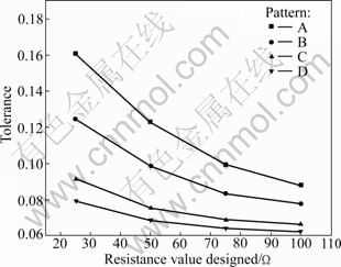
Fig.6 Manufacturing tolerances for test patterns
In order to evaluate the control ability or the manufacturing stability for a fabrication processing, process capability index (Cp) is proposed to make a statement about how well the manufacturing process meets the specification target:
![]() (4)
(4)
A capable process is one where almost all the measurements fall inside the specification limits. If the resistance value range is limited in 10% from the design target, the abilities of the manufacturing control Cp for the integrated resistors are given by totally 960 pieces resistors, as shown in Fig.7. The manufacturing process of the integrated resistors is a unique combination of equipments, materials, methods, and people engaged in. All manufacturing processes in the experiment have statistical variability which can be expressed by statistical methods [13]. The process capabilities in the experiment are from about 0.6 to 1.6 for the designed test patterns, which shows that the manufacturing process capabilities are sufficient for patterns C and D with larger value resistors, eligible for patterns B and C with middle value resistors, and inadequate for pattern A and smaller resistors [14].
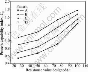
Fig.7 Process capability for manufacturing integrated resistors
Integrated passive technology provides component density beyond the physical capability of discrete like devices. But, there is little chance to repair the integrated passives, which is the challenge for the manufacturing process to prepare higher quality product. The integrated resistors fabricated here have reached sufficient quality in consistency, yield and manufacturing tolerance in the gross. The process capability shows that this manufacturing process can be used to fabricate the integrated resistors in multiple layer PCBs in the future. At present, other barriers to this technology include the limitation ranges for resistance values, relatively expensive fabrication processes, no design tools available and little knowledge about integrated passive characteristics in multilayer PCBs, such as heat dissipation. The commercial implementation of the integrated passive technology is a long way [15-17].
5 Conclusions
1) The fabrication processing of integrated resistors by lamination method was investigated in detail. Six major steps were given.
2) The test results for integrated resistors show the quality, such as the consistency, product yield and manufacturing tolerance, will increase with both the resistors size increasing (from 250 μm×125 μm to 1 000 μm×2 000 μm in width and length) and the resistance values increasing (from 25 to 100 Ω).
3) From the process capabilities, the manufacturing process capabilities are sufficient for patterns C and D with larger resistors, eligible for patterns B and C with middle resistors, and inadequate for pattern A with smaller resistors.
References
[1] JEONG I, KIM K J, KONG T O, KIM J S, CHOI H K, NAM C M, KIM D W, KWON Y S. High performance RF integrated passive devices on thick oxide substrate using Cu-BcB process [J]. Microwave and Optical Technology Letters, 2003, 37(1): 49-52.
[2] JILLEK W, YUNG W K C. Embedded components in printed circuit boards: A processing technology review [J]. International Journal of Advanced Manufacturing Technology, 2005, 25(3): 350-360.
[3] ZHOU J M, MYERS J D, FELTEN J J. Embedded passives technology for PCBs: Materials, design, and process [C]// Proceedings of the Society of Photo-optical Instrumentation Engineers (SPIE). Denver: 2002: 577-582.
[4] YANG J, UME I C. Thermomechanical reliability study of flip chip solder bumps: Using laser ultrasound technique and finite element method [J]. IEEE Transactions on Advanced Packaging, 2009, 32(4): 729-739.
[5] MUTHANA P, SRINIVASAN K, ENGIN A E, SWAMINATHAN M, TUMMALA R, SUNDARAM V. Improvements in noise suppression for I/O circuits using embedded planar capacitors [J]. IEEE Transactions on Advanced Packaging, 2008, 31(2): 234-245.
[6] MIN G. Embedded passive resistors: Challenges and opportunities for conducting polymers [J]. Synthetic Metals, 2005, 153(2): 49-52.
[7] BRANDLER D D. The effect of miniaturization on embedded resistors in high density interconnecting substrate [C]// Proceedings of International Symposium on Microelectronics (SPIE). Baltimore, 2001: 464-466.
[8] HSI C S, HSIEH F M, CHEN H P. Characteristics of thick film resistors embedded in low temperature co-fired ceramic (LTCC) substrates [J]. Journal of the European Ceramic Society, 2007, 27(9): 2779-2784.
[9] SALZANO L J, WILKINSON C, SANDORON P A. Environmental qualification testing and failure analysis of embedded resistors [J]. IEEE Transactions on Advanced Packaging, 2005, 28(3): 503-520.
[10] MORI T, YAMAGUCHI M, KURAMOCHI S, FUKUOKA Y. Development of a new interposer including embedded thin film passive elements [J]. IEEE Transactions on Advanced Packaging, 2009, 32(2): 503-508.
[11] CHENG P L, LEUNG Y Y, LAW T W, LIU C K, CHONG I T, LAM C C. Quantitative analysis of resistance variations in nickel- phosphorus (NiP) resistors [J]. IEEE Transactions on Components and Packaging Technologies, 2007, 30(2): 264-268.
[12] LI Chun-hao, TSAI Ming-jong. 3D laser trimming technology for regulating embedded thick-film carbon resistors on a random access memory module [J]. Journal of Materials Processing Technology, 2009, 209(4): 2057-2067.
[13] SHI Lin-chu. The application of mathematic-statistical method in IC mass production-on the relationship between processing capability index and yield [J]. Acta Electronica Sinica, 1998, 26(5): 125-128. (in Chinese)
[14] WU C W, PEARN W L, KOTZ S. An overview of theory and practice on process capability indices for quality assurance [J]. International Journal of Production Economics, 2009, 117(2): 338-359.
[15] WANG Hui, GU Guo-hua, QI Yun-feng. Crushing performance and resource characteristic of printed circuit board scrap [J]. Journal of Central South University of Technology, 2005, 12(5): 552-555.
[16] CHAI Li-yuan, YOU Xiang-yu, SHU Yu-de, YANG Jie, WANG Yun-yan. Decoppering of copper-complexing wastewater from printed circuit boards [J]. Journal of Central South University: Science and Technology, 2010, 41(1): 27-33. (in Chinese)
[17] QIU Ke-qiang, WU Qian, ZHAN Zhi-hua. Vacuum pyrolysis characteristics of waste printed circuit boards epoxy resin and analysis of liquid products [J]. Journal of Central South University: Science and Technology, 2009, 40(5): 1209-1215. (in Chinese)
(Edited by YANG Bing)
Foundation item: Project(041010) supported by Start-Up Foundation of Northwest University, China; Project(UIT/39) supported by University-Industry Collaboration Program from the Innovation and Technology Fund of Hong Kong, China
Received date: 2010-03-10; Accepted date: 2010-09-28
Corresponding author: WANG Shou-guo, Associate Professor, PhD; Tel: +86-29-88303381; E-mail: apwangsg@tom.com

