


Trans. Nonferrous Met. Soc. China 22(2012) 1151-1155
Microstructure evolution of copper doped beryllium thin films
ZHOU Min-jie, LUO Bing-chi, LI Kai, ZHANG Ji-cheng, LI Jia, WU Wei-dong
Research Center of Laser Fusion, China Academy of Engineering Physics, Mianyang 621900, China
Received 31 May 2011; accepted 25 October 2011
Abstract: Copper (Cu) doped beryllium (Be) thin films were deposited on silicon substrates by using a simple ion beam sputtering method, which can also realize the varying of Cu doping concentration. Detailed morphological and structural characterizations of the samples clearly disclose a microstructure evolution of films upon doping Cu. Doping Cu can effectively suppress film grain growth, causing a small grain size as well as uniform size distribution. Furthermore, doping Cu affects the crystallographic texture of film, which leads to the formation of more compact film structure. In particular, the surface smoothness of the doped films is significantly improved, which makes them promising candidates for various applications.
Key words: beryllium; thin films; Cu doping; microstructure
1 Introduction
Beryllium (Be), one of the lightest elements (Atomic number Z=4), has long attracted great research interests because of its unique atomic structure and excellent physical properties [1,2]. Beryllium exhibits a number of technologically significant characteristics, including low mass density, low absorption for X-ray, low Poisson ratio, high elastic modulus and special alloying properties. Indeed, it has played an important role in nuclear power industry, aeronautics, mechanics, electronics and inertial confinement fusion experiments [3-7]. In particular, Be thin films are of special interests and many research efforts have been devoted to the synthesis, characterization, properties investigation of Be thin films [8-12]. It is known that the structure is a key factor that governs thin film properties, and the practical use of film requires fundamental knowledge on structure formation and structure evolution mechanism, which is crucial for tailoring thin film properties. Besides synthesis conditions, elemental doping is also an effective way to affect the microstructure of thin film, and thus leads to desired film properties [13,14]. Although doped Be film has received much attention [15,16], those researches focus on Be film with quite large thickness (~100 μm) and quite low doping content (<1% in mole fraction). In short, the study on modifying microstructure of Be thin film by elemental doping with a wider range is still rather limited, which is of both basic scientific and technological interests. In the present work, a series of beryllium films with different copper content are deposited by using a simple ion beam sputtering method. Chemical composition, microstructure, crystallinity and surface roughness of the films are examined, and it is found that doping copper strongly affects the microstructure of Be films. The evolution of the film surface roughness as a function of the copper doping content is correlated to the change of its grain size, size uniformity and crystallographic texture.
2 Experimental
A high vacuum system equipped with two 3 cm Kaufman-type ion guns (Ion Tech., model 3-1500-100) was employed to deposit copper doped beryllium thin film samples. The base pressure of the chamber was below 1.3×10⁻⁴ Pa. The Si (001) substrates were in-situ pre-sputter-cleaned using argon ion (Ar+) beam (40 mA, 500 eV) before deposition. A high purity (99.5%) 4-inch (10.16 cm) beryllium target was used as a source material, and small Cu chips were fixed onto the Be target surface as mixed target for doped samples. The Cu doping content was manipulated by adjusting the quantity of Cu chips. During deposition, an Ar+ beam (operating at 60 mA and 1000 eV) generated by the ion gun sputtered the target and contributed to the film deposition. The duration for the thin film deposition was kept 30 min for all samples. In total, a pure Be thin film and three doped samples with different Cu contents were deposited as sample series.
The chemical composition of samples was examined on a X-ray photoelectron spectroscope (XPS; PHI Quantum 2000). Detailed information of the films’ microstructure was studied on a transmission electron microscope (TEM; JOEL 2010 FEG) with electron energy loss spectrometer (EELS, GIF) attached to the same microscope. Cross-section TEM sample was prepared by a focused ion beam (FIB) liftout technique [17], with a Pt protective layer deposited on the film surface. The general morphology and crystallinity of the films were investigated by scanning electron microscope (SEM; Quantum F400) and X-ray diffraction (XRD; Ragiku RU300), respectively. The film surface roughness was examined on a white light interferometer (Zygo NewView7000).
3 Results and discussion
The chemical compositions of all the thin films were examined by XPS and typical results are shown in Fig. 1. The films were sputtered off 20 nm to remove the surface contamination layer. Survey scan spectra reveal that all of the samples are high purity beryllium films with copper dopants. Fine scans were performed on both Be 1s and Cu 2p regions in order to find out the compositional binding states and copper doping content in the films. It is found that the peak centered at 111.8 eV can be observed in the Be 1s region, which corresponds metallic Be. For the feature observed in Cu 2p region, two peaks centered at 932.6 eV and 952.2 eV can be assigned to the metallic copper 2p3/2 and 2p1/2 peaks, respectively. Quantitative analysis reveals that copper contents of three samples are 0.8%, 2.1% and 4.5% (mole fraction), respectively, confirming the successful tuning of film composition.
The microstructure of film is disclosed by cross-sectional TEM study, and typical results are shown in Fig. 2. The full film can be seen in the image with Si substrate and Pt protective layer visible on the right and left (Fig. 2(a)), from which the film thickness is estimated at ~100 nm. High-resolution TEM image suggests the polycrystalline nature of the film (Fig. 2(b)). Furthermore, Be K-edge and Cu L-edge were used for EELS elemental mapping (Fig. 2(c) and Fig. 2(d)), by which the correlation between Be and Cu distribution in the film can be established. Both Be and Cu mapping images show quite homogeneous contrast in film region, indicating a fairly uniform Cu doping in the Be films over the whole area.
The surface of all films was examined by SEM, which gives a sense of the change in morphology films under the effect of Cu doping. Six-fold hexagonal pattering grains can be clearly observed in the pure Be film (Fig. 3(a)), and the grain size is found to be ~200 nm. Such hexagonal geometry becomes much less discernable due to Cu doping (Fig. 3(b)), which also leads to a grain size decreasing to ~150 nm. With the Cu doping content increases to 2.1%, the film surface exhibits a dense and faceted structure (Fig. 3(c)), and the grain size significantly reduces to ~50 nm. Further increase in the Cu doping content to 4.5% also shows faceting feature (Fig. 3(d)), while results in a more compact surface structure and smaller grain size of ~30 nm.
The crystallinity of all the films has been examined by XRD, and a structural evolution with Cu doping is observed. The XRD pattern of pure Be film can be indexed by assigning a hexagonal lattice (Fig. 4(a)), in which (100), (002), (101) and (012) reflections can be identified. Although no reflections corresponding to Cu phase can be detected due to the relatively low doping content (0.8%), Cu doping effectively suppresses the intensity of (002) reflection (Fig. 4(b)). When the Cu doping content increases to 2.1%, the Be (002) peak becomes trivial, and a broad Cu (111) peak is detected (Fig. 4(c)). The Be (002) reflection eventually disappears when the Cu doping content increases to 4.5% (Fig. 4(d)), while the Cu (111) reflection becomes more distinctive. No other phase was detected for all films in XRD patterns, excluding possible sample contamination and oxidation during the synthesis process.
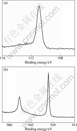
Fig. 1 XPS results of 4.5% Cu doped Be thin film: (a) Be 1s core level spectrum; (b) Cu 2p core level spectrum
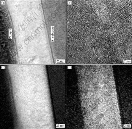
Fig. 2 Cross sectional low magnification TEM image (a) and high resolution TEM image (b), Be EELS mapping image (c), and Cu EELS mapping image of Be thin film with 4.5% Cu doping (d)
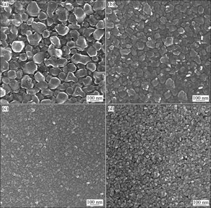
Fig. 3 SEM images of Be thin films with different Cu doping contents: (a) 0%; (b) 0.8%; (c) 2.1%; (d) 4.5%
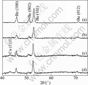
Fig. 4 XRD patterns of Be thin films with different Cu doping contents: (a) 0%; (b) 0.8%; (c) 2.1%; (d) 4.5%
To understand the films in more detail, surface roughness measurements were performed. The results also show a strong dependence on the Cu doping content. The root mean square roughness of the films as a function of the Cu doping content is plotted in Fig. 5. As the Cu content of the film increases, the surface roughness film first decreases drastically, and then declines slightly at further increased Cu content.
Based on the microstructural observations, it is evident that Cu doping has a significant effect on the film growth morphology. The pure Be film can grow with basal texture, leading to the six-fold hexagonal pattering grains observed in the SEM image. Cu doping effectively prevents the film from growing on (002) basal plane, and results in the faceted surface morphology of doped film. It is also interesting to note the film grain size dependence on the Cu content. Large grain size and wide size distribution are observed for the film without Cu introduction. Both drop in the grain size and rise in the size uniformity occur at Cu content increasing to 2% and above. Although the amount of Cu doped into the Be films is still low, i.e., clear separation between the Be grains and Cu is never large enough to be observed in the TEM investigation, the Cu atoms indeed suppress the grain growth in the Be films, and narrow the grain size distribution. Correspondingly, finer grains and more uniform grain size lead to the formation of a more compact film structure, as well as a more smooth film surface.
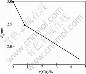
Fig. 5 Root mean square roughness (Rq) of Be thin films as function of Cu doping content
4 Conclusions
Be thin films with different Cu doping contents were deposited on silicon substrates using a simple ion beam sputtering method. Cu doping has significant effects on the microstructure of Be film. The Cu dopants effectively suppress grain from growth, causing a small grain size as well as uniform size distribution. Furthermore, Cu doping depresses (002) direction growth, which results in a transition from hexagonal patter to faceted structure of film surface morphology. All these factors contribute to the improved surface smoothness of the doped film.
Acknowledgements
The authors are grateful to Prof. CUI Xu-dong and Mr. HAN Shang-jun for their technical help and useful discussions.
References
[1] ROBERT G, LEGRAND P, BERNARD S. Multiphase equation of state and elastic moduli of solid beryllium from first principles [J]. Physical Rewiew B, 2010, 82: 104118.
[2] NADAL M H, BOURGEOIS L. Elastic moduli of beryllium versus temperature: Experimental data updating [J]. Journal of Applied Physics, 2010, 82: 033512.
[3] DITTRICH T R, HAAN S W, MARINAK M M, POLLAINE S M, HINKEL D E, MUNRO D H, VERDON C P, STROBEL G L, MCEACHEM R, COOK R C, ROBERTS C C, WILSON D C, BRADLEY P A, FOREMAN L R, VARNUM W S. Review of indirect-drive design options for the national ignition facility [J]. Physics of Plasmas, 1999, 6: 2164-2170.
[4] HAAN S W, AMENDT P A, DITTRICH T R, HAMMEL B A, HATCHETT S P, HERRMANN M C, HURRICANE O A, JONES O S, LINDL J D, MARINAK M M, MUNRO D, POLLAINE S M, SALMONSON J D, SRROBEL G L, SUTER L J. Design and simulations of indirect drive ignition targets for NIF [J]. Nuclear Fusion, 2004, 44: S171-S176.
[5] XU De-mei, QIN Gao-wu, LI Feng, WANG Dong-xin, XIA Hong-xian, REN Yu-ping, PEI Wen-li. Effects of morphology and distribution of BeO impurity on mechanical properties of metal beryllium [J]. The Chinese Jounal of Nonferrous Metals, 2011, 21(4): 769-776. (in Chinese)
[6] ZHANG Qing-lai, BONDAREV A B, ANDREEV V A, WANG Li-li, HU Yong-xue. Effect of aging treatment on residual resistance ration of beryllium [J]. The Chinese Jounal of Nonferrous Metals, 2007, 17(7): 1124-1128. (in Chinese)
[7] ZHONG Jing-ming, WANG Zhan-hong, NIE Da-jun, MIN Xue-ren, WANG Xue-ze, FU Xiao-xu, WANG Ling-sen. Influence of grain size on mechanical properties of isostatically pressed beryllium materials [J]. Transactions of Nonferrous Metals Society of China, 2000, 10(2): 228-231.
[8] HEIEH E J, PRICE C W, PIERCE E L, WIRTENSON R G. Effect of nitrogen pulsing on sputter-deposited beryllium [J]. Journal of Vaccum Science & Technology A, 1990, 8: 2165-2168.
[9] JANKOWSKI A F, WALL M A, BUREN V, NIEH T G, WADSWORTH J. From nanocrystline to amorphous structure in beryllim-based coatings [J]. Acta Materialia, 2002, 50: 4791-4800.
[10] LUNGU C P, MUSTATA I, ZAROSCHI V, LUNGU A M, CHIRU A, ANGHE G, BURCEA G, BAILESCU V, DINUTA G, DIN F. Spectroscopic study of beryllium plasma produced by thermionic vacuum arc [J]. Journal of Optoelectronics and Advanced Materials, 2007, 9: 884-886.
[11] ANGHEL G, MUSTATA I, POROSNICU C, LUNGU C P. Influence of the bias voltage on the formation of beryllium films by thermionic vacuum arc method [J]. Journal of Nuclear Materials, 2009, 385: 242-245.
[12] WILTNER A, LINSMEIER C. Surface alloying of thin beryllium films on tungsten [J]. New Journal of Physics, 2006, 8: 181.
[13] RAUF L A, YUAN J. Effects of microstructure on the optical properties of tin-doped indium oxide thin films studied by electron energy loss spectroscopy [J]. Materials Letters, 1995, 25: 217-222.
[14] CHENG Chuan-pin, TANG Ming-hua, YE Zhi, ZHOU Yi-chun, ZHENG Xue-jun, HU Zen-shun, HU He-ping. Microstructure and ferroelectric properties of dysprosium-doped bismuth titanate thin films [J]. Materials Letters, 2007, 61: 4117-4120.
[15] NIKROO A, CHEN K C, HOPPE M L, HUANG H, WALL J R, XU H, MCELFRESH M W, ALFORD C S, COOK R C, COOLEY J C, FIELDS R, HACKENBERG R, DOERNER R P, BALDWIN M. Progress toward fabrication of graded doped beryllium and CH capsules for the national ignition facility [J]. Physics of Plasmas, 2006, 13: 056302.
[16] XU H W, ALFORD C S, COOLEY J C, DIXON L A, HACKENBERG R E, LETTS S A, MORENO K A, NIKROO A, WALL J R, YOUNGBLOOD K P. Beryllium capsule coating development for NIF targets [J]. Fusion Science and Technology, 2007, 4: 547-552.
[17] MAYER J, GIANNUZZI L A, KAMINO T, MICHAEL J. TEM sample preparation and FIB-induced damage [J]. MRS Bulletin, 2007, 32: 400-407.
Cu掺杂对Be薄膜微结构的影响
周民杰,罗炳池,李 恺,张继成,李 佳,吴卫东
中国工程物理研究院 激光聚变研究中心,绵阳 621900
摘 要:利用离子束溅射法在硅基底上制备高纯Be薄膜并实现Cu元素的可控掺杂,利用X射线能谱、扫描电镜、X射线衍射以及透射电镜等对Cu掺杂Be薄膜进行表征分析。研究结果表明:Cu元素在Be膜内分布均一,且Cu掺杂量对Be薄膜的微观结构有显著影响。Cu掺杂能抑制Be晶粒生长,Be晶粒随着薄膜中Cu含量的增多而减小,并且尺寸分布更加均匀;Cu掺杂影响Be晶粒的生长取向,使其形成更为紧凑的薄膜结构。这些因素使得掺杂Cu的Be薄膜的表面粗糙度明显降低。
关键词:铍;薄膜;铜掺杂;微结构
(Edited by YANG Hua)
Foundation item: Project (60908023) supported by the National Natural Science Foundation of China
Corresponding author: WU Wei-dong; Tel/Fax: +86-816-2480830; E-mail: lrcwuweidong@gmail.com
DOI: 10.1016/S1003-6326(11)61298-3