Properties of nanocrystalline copper prepared by vacuum-warm-compaction method
CHU Guang(楚 广)1, 2, LIU Wei(刘 伟)1, YANG Tian-zu(杨天足)1, TANG Yong-jian(唐永建)2
1. School of Metallurgical Science and Engineering, Central South University, Changsha 410083, China;
2. Research Center of Laser Fusion of CAEP, Mianyang 621900, China
Received 15 April 2008; accepted 15 October 2008
Abstract: Nanocrystalline Cu with average grain size of 22.8-25.3 nm was prepared by vacuum-warm-compaction method. Scanning electronic microscope, HMV-2 type microhardness tester, X-ray diffractometer, and 6157 type electrometer were used to determine the microstructure, microhardness and electrical resistivity of as-prepared nanocrystalline Cu, respectively. The results show that the microhardness of nanocrystalline Cu increases with larger pressure, longer duration of pressure or higher temperature. The highest microhardness of nanocrystalline Cu is 3.8 GPa, which is 7 times higher than that of coarse-grained copper. The electrical resistivity of as-prepared specimens is (1.2-1.4)×10-7 Ω・m at temperature 233-293 K, which is 5-6 times higher than that of the coarse-grained copper.
Key words: vacuum-warm-compaction; nanomaterials; microhardness; electrical resistivity
1 Introduction
Nanocrystalline bulk materials are three- dimensional solid ones, which are composed of nano-sized grains or crystallites. The grain size is so small (<100 nm) that a large amount of atoms exist in the grain boundary, and the proportion of grain boundary is large up to 50%. Nanocrystalline materials have remarkable properties owing to their unique structure [1-8]. In recent years, there is growing interest in synthesis of nanocrystalline materials for the nanocrystalline materials can be widely used unless they could be prepared by easy and efficient methods. There are many approaches to synthesize nanocrystalline materials, such as inert gas condense in-site compaction [1,4], mechanical alloying[5], electrical deposition[2], serve plastic deformation[8-9]. Among these methods, flow-levitation-cold-compaction method(FLCC)[10-12] has advantages of few investment and convenient operation, but the density of the specimens is relatively low because the compaction process of FLCC is under 105 Pa (Ar) and at room temperature, which results in amounts of pores existing in the specimen. Vacuum-pumping and specimen-heating before and during compaction will cause gas desorption and accelerate atom diffusion, so vacuum-warm- compaction method(VWC) is an improvement of FLCC. The properties of nanocrystalline materials prepared by VWC should be better.
In this work, nanocrystalline Cu with grain size smaller than 30 nm was prepared by VWC. The compaction parameters were studied carefully to identify their influence upon the microhardness of the as-prepared specimens. The electrical resistivity of as- prepared nanocrystalline Cu was also studied.
2 Experimental
Nano-sized Cu particles were prepared by flow-levitation method[13] and then filled into the high strength mold in ZKSTX-1 type vacuum-glove-chest with Ar (purity>99.99%) protection. After the mold was put into the chamber of ZM-18-10Y type vacuum-hot- press, the chamber was pumped to a pressure of 1.3×10⁻⁴ Pa, and then the mold with nano-size Cu particles was heated for 30 min in order to release absorbed gas prior to pressing. Subsequently, the nano-sized Cu particles were compacted at 288-473 K, under a uniaxial load of 1.0-1.63 GPa for duration of 20-60 min, resulting in disc-shape samples with 10 mm in diameter and 0.5-1.5 mm in thickness.
A Philips X’Pert Pro MPD type X-ray diffractometer (made in Netherlands, Cu Kα radiation, λ=0.154 056 nm) was used to identify the phase of the specimens. The average grain size and average microstrain were measured according to XRD patterns with Warren-Averbach Fourier transfer method of (111), (200), (220) peaks. The density of the compacted samples was measured using Archimedes’ principle. Vickers microhardness measurements (HMV-2, standard error 0.2%) were taken 10 times on each specimen with 2 N load applied for 20 s. A 6157 type electrometer was used to measure the electrical resistivity of the samples at 233-293 K. A JSM-6360LV scanning electronic microscope(SEM) was employed to observe the microstructure of as-prepared specimens.
3 Results and discussion
3.1 Density and grain size
The as-prepared nanocrystalline Cu has a smooth surface without cracks and rough edge. The relative density of nanocrystalline Cu in this work is 94%-96%. Compared with that of nanocrystalline Cu prepared by FLCC (85%-93%[10]), the density is improved evidently. Fig.1 shows the SEM image of nanocrystalline Cu prepared under a pressure of 1.5 GPa. In this photograph, the fine nano-particles congregate under high pressure and the average particle size of the specimen is smaller than 300 nm. Because of the high surface energy of nano-particles, the density of nanocrystalline materials prepared by similar method, such as IGC, cannot reach 100%[1, 4, 10 ]. As shown in Fig.1, although the consolidation is firm, there are still some micro-pores in the specimen.

Fig.1 SEM image of nanocrystalline Cu
Table 1 lists the average grain size and microstrain of specimen at different compacting temperature (all these nanocrystalline Cu were prepared under pressure of 1.63 GPa with duration of 60 min).
Table 1 Average grain size and microstrain of specimen at different compacting temperatures

3.2 Microhardness
Generally speaking, the density of nanocrystalline Cu will increase during compaction[11]. The density of nanocrystalline Cu (94%-96%) compacted at higher temperature is larger than that of the counterparts (85%- 93%) compacted at room temperature. This is due to the following two reasons. Firstly, the adsorbed gas can be desorbed easily when heated; the number of micro-pores became less. Secondly, the diffusion rate of atoms increases at the elevated temperature.
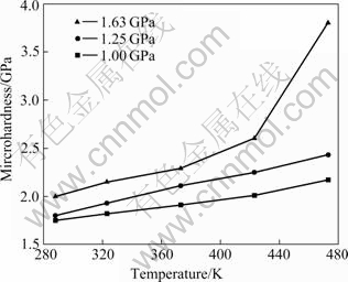
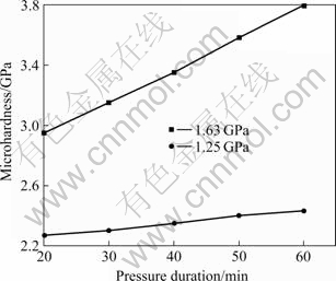
Figs.2-4 show the microhardness of as-prepared nanocrystalline Cu influenced by the parameters of pressure, temperature, and pressure-keeping time, respectively. These figures show the microhardness of nanocrystalline Cu increases with increasing pressure and temperature and prolonging pressure-keeping time, resulting in less micro-pores inside the specimens and a modified distribution of residual stress.

Fig.2 Curves of microhardness vs pressure (pressure-keeping time 60 min) at different temperatures

Fig.3 Curves of microhardness vs temperature (60 min)

Fig.4 Curves of microhardness vs pressure duration (temperature 473 K)
There is a manifest increase of microhardness when the pressure is above 1.25 GPa and the temperature is higher than 473 K. For example, the microhardness of the specimen prepared under 1.25 GPa and 473 K is 2.4 GPa, while the microhardness even reaches 3.8 GPa when the specimen is compacted under 1.63 GPa and 473 K, which is 7 times higher than that of the coarse- grained counterparts (the microhardness of coarse- grained Cu is 0.45 GPa under the same test conditions). So, higher temperature and higher pressure are essential to prepare higher microhardness nanocrystalline Cu. Just as shown in Fig.4, even the specimen is compacted for only 20 min under 1.63 GPa and 473 K, the microhardness can reach 2.8 GPa, which is higher than that of the other specimens compacted for 60 min with smaller pressure or below 473 K.
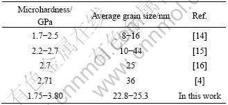
In Fig.3, it also can be found that the microhardness of nanocrystalline Cu prepared by VWC is much higher than that by FLCC. This indicates that vacuum-pump and warm-compaction are useful to synthesize better nanocrystalline materials. Compared with the data in other literatures listed in Table 2, the microhardness of as-prepared nanocrystalline Cu in this work is very high.
Table 2 Microhardness of nanocrystalline Cu in different literatures

The grain size has a profound effect on the mechanical behavior of materials, in particular, on the yield stress and hardness. The Hall-Petch relationship[17] is a well-known expression relating the variation in yield stress to the grain size of a material:
σy=σ0+kd-1/2 (1)
where σy is the yield stress; σ0 is the lattice friction stress required to move individual dislocation; k is a constant and d is the grain size. The form of the equation indicates that a decrease in grain size will lead to an increase in the yield strength. According to the Hall-Petch equation, large yield strength may be attained by reducing the grain size of materials. For example, a drop in average grain size from 10 μm to 10 nm should increase the yield stress more than thirty-fold.
For pyramidal indenters, the microhardness(Hv) of metals is empirically related to the yield stress(σ0) by the relation Hv/σ0=3[17]. For material that exhibits Hall- Petch behavior, the hardness Hv should be related to grain size d, as
Hv≈H0+kHd-1/2 (2)
where H0 and kH are constants. In Ref.[17], the microhardness of nanocrystalline Cu with average grain size of 25 nm is about 2.4 GPa, which is a bit lower than that in this work. As the grain size is the same, the difference derives from the synthesis process. The nanocrystalline Cu prepared by VWC method has better quality. Considering that the density of nanocrystalline Cu in this paper is not 100%, it is expected that the microhardness of fully dense and fully relaxed nanocrystalline-materials will be much higher.
In this work, the average grain size varied so little that it is hard to draw any conclusion about the relationship between the microhardness and the grain size. It is an interesting work to prove whether the relationship between the microhardness and grain size obeys the classical Hall-Petch equation. In recent years, many researches have been done in this field[17-18], but the experimental results of even the same nanocrystalline metal may be discrepancy due to different synthesis process. As discussed above, the microhardness is influenced by micro-defects largely; it increases when the number of the micro-pores becomes less. In our opinion, the specimens are comparable only when their conditions (such as the density and stress distribution) are same. Such task is under researching and will be reported later.
Table 3 Calculation results of ρ0 and α

3.3 Electrical resistivity
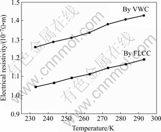
The electrical resistivity of nanocrystalline metals was usually higher than that of coarse-grained counterparts[19]. There is large grain boundary region in the nanocrystalline materials and the activities of electrons are restricted around the small nano- crystallines. The thicker the grain boundary is, the more disorderly the grains array and the more strongly the electrons scatter. So the electrical resistivity of nanocrystalline metals is usually high. Fig.5 shows the temperature (233-293 K) dependence of the electrical resistivity of nanocrystalline Cu specimens prepared by VWC (at 473 K) and FLCC (at room temperature), respectively. The electrical resistivity of nanocrystalline Cu at room temperature is (1.2-1.4)×10-7 Ω・m, which is in a reasonable quality compared to the experimental results of QIAN et al[20]. The electrical resistivity is 5-6 times higher than that of the coarse-grained Cu (0.2×10⁻⁷ Ω・m).

Fig.5 Temperature dependence of electrical resistivity of as- prepared nanocrystalline Cu
From Fig.5, it can be found that the electrical resistivity is higher when the specimens are prepared by VWC method. This is due to the difference in synthesis methods, which leads to different microstructure of the nanocrystalline specimens. This phenomenon just indicates that the high electrical resistivity is the inherent property of nanocrystalline metals.
The relationship between the electrical resistivity and measuring temperature (233-293 K) fits the Matthissen equation[19]:
ρ=ρ0(1+αT) (3)
where ρ0 is the electrical resistivity at absolute zero, α is the temperature coefficient, and T is temperature. The calculation results of ρ0 and α are listed in Table 3. The value of α is lower than the reported value in Ref.[20]. This indicates that the electrical resistivity varies insignificantly when the temperature changes. In other words, grain boundary scatting is the main mechanism affecting the electron transport. This phenomenon may relate with the microstructure of nanocrystalline metals and needs further researches.
4 Conclusions
Nanocrystalline copper with the average grain size of 22.8-25.3 nm was prepared by vacuum-warm- compaction method. The microhardness of the as-prepared nanocrystalline Cu can reach 3.8 GPa, which is 7 times higher than that of the coarse-grained copper. The microhardness increases with increasing the pressure, the duration and the temperature. The as-prepared nanocrystalline Cu has a good thermal stability. The grain size grows insignificantly at relative lower temperature (<473 K). The electrical resistivity of the as-prepared nanocrystalline Cu at room temperature is (1.2-1.4)× 10-7 Ω・m, which is 5-6 times higher than that of the coarse-grained counterparts (0.2×10⁻⁷ Ω・m).
References
[1] GLEITER H. Nanocrystalline materials [J]. Prog Mater Sci, 1989, 33: 223-315.
[2] LU L, SUI M L, LU K. Superplastic extensibility of nanocrystalline copper at room temperature [J]. Science, 2000, 287: 1463-1466.
[3] CHAMPION Y, GUERIN-MAILLY S, BONNENTIEN J L, LANGLOIS P. Fabrication of bulk nanostructured materials from metallic nanopowders: Structure and mechanical behavior [J]. Scripta Mater, 2001, 44: 1609-1613.
[4] ZHOU Y S, WU X J, XU G L, LI B H, ZHANG H F, DU L G, LI Z Q. Synthesis, microdefects and mechanical properties of large bulk nanocrystalline silver and copper [J]. The Chinese Journal of Nonferrous Metals, 2000, 10(4): 465-469. (in Chinese)
[5] KRASNOWSKI M, ANTOLAK A, KULI T. Nanocrystalline Ni3Al alloy produced by mechanical alloying of nickel aluminides and hot-pressing consolidation [J]. Journal of Alloys and Compounds, 2007, 434/435: 344-347.
[6] SWYGENHOVEN H V. Grain boundaries and dislocations [J]. Science, 2002, 296: 66-67.
[7] CHEN J, LU L, LU K. Hardness and strain rate sensitivity of nanocrystalline-Cu [J]. Scripta Mater, 2006, 54: 1913-1918.
[8] WEI Q, JIAO T, RAMESH K T, MA E, KECSKES L J, MAGNESS L, DOWDING R, KAZYKHANOV V U, VALIEV R Z. Mechanical behavior and dynamic failure of high-strength ultrafine grained tungsten under uniaxial compression [J]. Acta Mater, 2006, 54: 77-87.
[9] VALIEV R Z, ISLAMAGALIEV R K, ALEXANDROV I V. Bulk nanostructured materials from severe plastic deformation [J]. Prog Mater Sci, 2000, 45: 103-189.
[10] CHU G, TANG Y J, LUO J S, LIU W, YANG T Z, LI J, HONG W. Preparation synthesis of nanocrystalline copper target material for ICF experiments [J]. High Power Laser and Particle Beams, 2005, 17: 1829-1834.
[11] CHU G, LIU W, LUO J S, TANG Y J, LI J, SHI H L, YANG T Z. Effects of processing parameters on properties of nanocrystalline Cu [J]. High Power Laser and Particle Beams, 2005, 17: 1701-1704.
[12] LIU W, TANG Y J, CHU G, LUO J S, YANG S Y, LI J, WU W D. Research on microhardness and microstructure of nanocrystalline Cu [J]. Materials Science and Technology, 2006, 14: 127-130.
[13] LI C M, LEI H, TANG Y J, LUO J S, LIU W, CHEN Z M. Production of copper nanoparticles by the flow-levitation method [J]. Nanotechnology, 2004, 15: 1866-1869.
[14] FOUGERE G E, WEERTMAN J R, SIEGEL R W, KIM S. Grain-size dependent hardening and softening of nanocrystalline Cu and Pd [J]. Scripta Metall Mater, 1992, 26: 1879-1883.
[15] CHOKSHI A H, RISEN A, KARCH J, GLEITER H. On the validity of the Hall-Petch relationship in nanocrystalline materials [J]. Scripta Metall Mater, 1989, 23: 1679-1684
[16] YANG M C, YE F, SUN X C, SUN X K, WEI W D. Study on the microhardness of bulk nanocrystalline copper [J]. Nanostr Mater, 1997, 9: 481-484.
[17] NIEMAN G W, WEERTMAN J R. Mechanical behavior of nanocrystalline Cu and Pd [J]. J Mater Res, 1991, 6(5): 1012-1027.
[18] AGNEW S R, ELLIOTT B T, YOUGDAHL C J, HEMKER K J, WEERTMAN J R. Microstructure and mechanical behavior of nanocrystalline metals [J]. Mater Sci Eng A, 2000, 285: 391-396.
[19] ZHANG L D, MOU J M. Nanomaterials and nanostructure [M]. Beijing: Science Press, 2002: 216. (in Chinese)
[20] QIAN L H, LUQ H, KONG W J, LU K. Electrical resistivity of fully-relaxed grain boundaries in nanocrystalline Cu[J]. Scripta Mater, 2004, 50: 1407-1411.
Foundation item: Project(10475069/A0506) supported by the National Natural Science Foundation of China
Corresponding author: CHU Guang; Tel: +86-731-8836791; Fax: +86-731-8710171; E-mail: chuguang2006@163.com
DOI: 10.1016/S1003-6326(08)60284-8
(Edited by YUAN Sai-qian)