Characteristics of Si+/B+ dual implanted silicon wafers
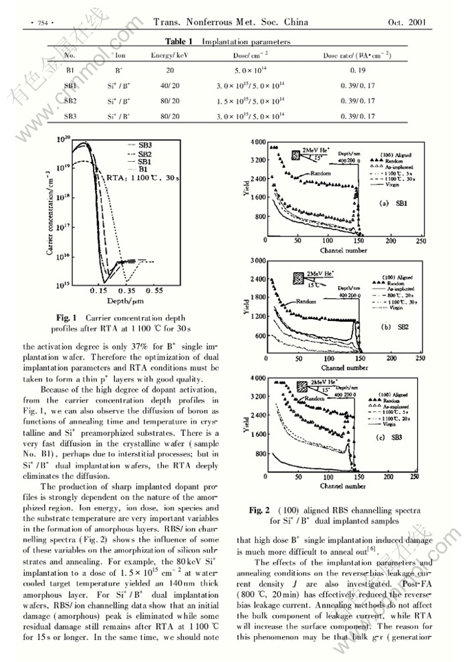
栖坿豚侵⦿嶄忽嗤弼署奉僥烏(哂猟井)2001定及5豚
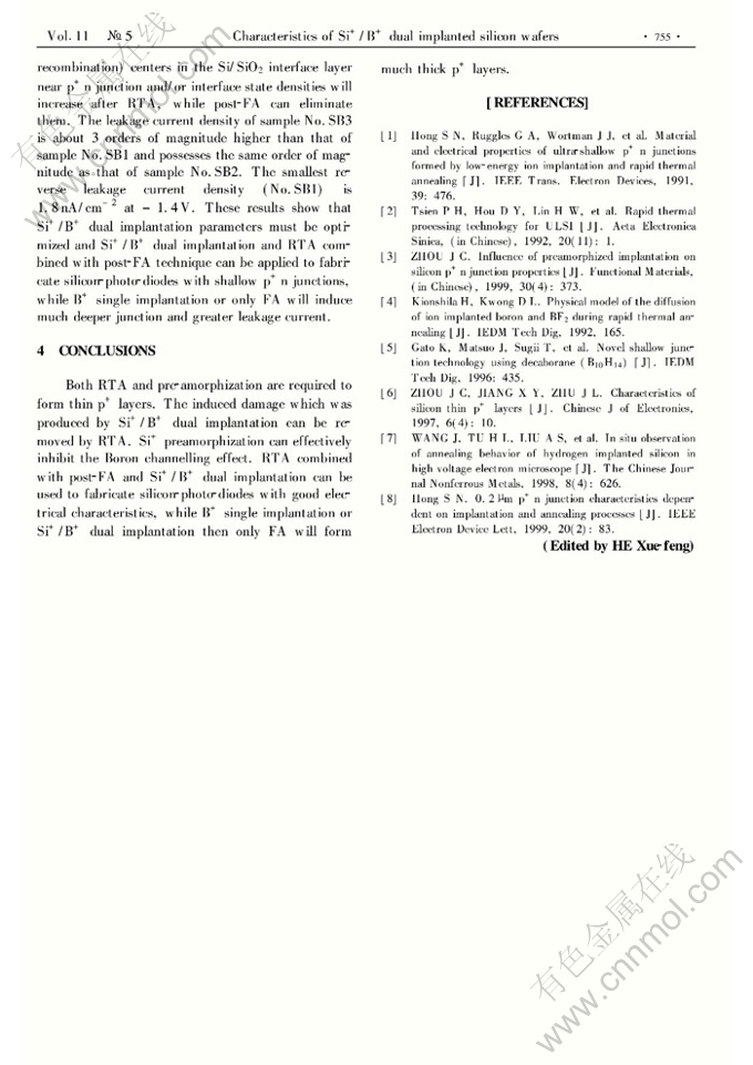
胎猟恬宀⦿巓写覚 仔荻堝
猟嫗匈鷹⦿753 - 755
Key words⦿rapid thermal annealing; dual ion implantation; silicon thin p+ layers
Abstract: Thin p+ layers with good electrical properties were fabricated by RTA (rapid thermal annealing) with post-FA (furance annealing) of Si+/B+ dual implanted silicon wafers. The electrical and structural characteristics of thin p+ layers have been measured by FPP (four-point probe), SRP (spreading resistance probe), RBS/channelling. Optimizing the implantation and annealing processes, especially using the thermal cycle of RTA followed by FA, shallow p+n junctions can be fabricated, which shows excellent I-V characteristics with reversšbias leakage current densities of 1.8nA/cm2Žat -1.4V.