文章编号:1004-0609(2009)05-0930-06
电沉积Ag/Sn偶界面反应及其动力学
汤文明1,HE An-qiang2, LIU Qi2, IVEY G D2
(1. 合肥工业大学 材料科学与工程学院,合肥 230009;
2. Department of Chemical and Materials Engineering, University of Alberta, EdmontonT6G 2G6, Canada)
摘 要:采用扫描电子显微镜(SEM)、电子能谱仪(EDS)、X射线衍射仪(XRD)对室温时效及125~225 ℃热处理的电沉积Ag/Sn偶反应区结构及相组成进行分析,研究Ag/Sn界面固相反应的动力学过程。研究表明:在刚电沉积的Ag/Sn偶中发生Ag/Sn界面固相反应,形成Ag3Sn;在室温时效过程中Ag3Sn层生长缓慢,但随着热处理温度的提高(125~200 ℃),Ag3Sn层生长速率显著提高;Ag/Sn界面固相反应为一扩散控制的反应过程,反应的激活能为70.0 kJ/mol。
关键词:电沉积;电子封装材料;界面反应;反应动力学
中图分类号:TQ 153.2;O 643.1 文献标识码:A
Interfacial reaction and its kinetics of electroplated Ag/Sn couples
TANG Wen-ming1, HE An-qiang2, LIU Qi2, IVEY G D2
(1. School of Materials Science and Engineering, Hefei University of Technology, Hefei 230009, China;
2. Department of Chemical and Materials Engineering, University of Alberta, EdmontonT6G 2G6, Canada)
Abstract: The microstructures and phases of reaction regions of the electroplated Ag/Sn couples were studied by using SEM, EDS and XRD, after the couples were aged at room temperature and annealed at 125-225 ℃ for various times. The interfacial reaction kinetics of the Ag/Sn couples was also investigated. The results show that in the as-deposited Ag/Sn couple, the reaction between Ag and Sn occurs to form a thin Ag3Sn layer distributed at the Ag/Sn interface. The growth of the Ag3Sn layer is much slow when the couple is aged at room temperature, however, dramatically increases with the annealing temperature (125-200 ℃). The interfacial reaction of the Ag/Sn couples follows a diffusion-controlled kinetics with activation energy of 70.0 kJ/mol.
Key words: electroplation; electronic packaging materials; interfacial reaction; reaction kinetics
电子器件中常见的导电金属(UBM),如Cu、Ni、Ag、Au 及其合金通常与用于电子封装的Sn基焊料中的Sn反应形成金属间化合物(IMCs)[1-4]。这些金属间化合物一般都是脆性的,且电阻较高,因此,过量的界面金属间化合物的形成不仅导致连接点力学性能显著降低,同时还改变了连接部位的电学特征[5-8]。Cu、Ni、Ag、Au等导电金属与Sn基焊料间反应区结构、相组成及反应动力学等信息是预测电子芯片与导电基底连接(Chip-to-substrate connections)的寿命及可靠性的基础[9]。
在Ag-Sn二元相图[10](图1)上,仅存在两种Ag-Sn金属间化合物,一是无序结构的Ag4Sn(ζ相),另一个是属正交晶系的短程有序的Ag3Sn(ε相)。SEN等[11]发现气相沉积Ag/Sn偶在室温条件下形成Ag3Sn,ARAI等[12]发现在电镀共沉积Ag-Sn合金中也只形成了Ag3Sn。然而,最近SUZUKI等[13]将Ag/Sn块状偶在硅油中经160~200 ℃热处理,获得了Ag3Sn和Ag4Sn反应产物,这是唯一获得Ag4Sn反应产物的研究报道。此外,相对于Cu/Sn及Au/Sn等系统而言,Ag/Sn界面固相反应的研究比较少,还没有反应动力学的研究报道。
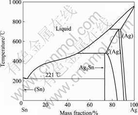
图1 Ag-Sn二元相图[10]
Fig.1 Ag-Sn binary phase diagram[10]
到目前为止,在研究Ag(Au、Cu、Ni)/Sn界面固相反应时,反应偶采用的是物理气相沉积方式形成的薄膜偶或将Ag(Au、Cu、Ni)片与Sn片叠合构成的块体偶。电镀沉积技术是在连接金属表面形成Sn基焊料焊点的主导技术,具有工艺简单、焊料成分可精确控制、有利于提高集成度等优势[14]。本文作者曾采用电镀技术制备出Au/Sn反应偶,并研究其反应区结构及反应动力学过程[15]。在此,本文作者采用电镀技术在金属化的Si晶片上制备Ag/Sn偶,研究Ag/Sn偶在室温时效及125~225 ℃热处理后Ag/Sn偶反应区的相组成及显微结构特征,并对反应区的生长动力学过程进行研究。
1 实验
实验采用C6H17N3O7-SnCl2・2H2O基Sn电镀溶液及AgNO3-NaSO3-NaS2O3基Ag电镀溶液。电镀Ag/Sn偶首先在金属化Si晶片上电镀一定厚度的Ag层,然后再电镀一定厚度的Sn层来制备。从直径为100 mm的Si晶圆片上切割而得的Si晶片尺寸为10 mm× 10 mm。Si晶圆片的金属化过程是首先在Si晶片上沉积厚25 nm的TiW 薄膜(90% W和10% Ti,质量分数)作为粘结层,再沉积厚200 nm的Pt膜作为籽晶层。
采用Dynatronix DuPR 10-0.1-0.3 脉冲电镀电源进行电镀,采用单脉冲电镀工艺,脉冲周期为10 ms,正向导通时间为2 ms,正向断开时间为8 ms。Sn电镀时的平均电流密度为25 mA/cm2,电镀速率约为0.5 μm/min;Ag电镀时的平均电流密度为1.5 mA/cm2,电镀速率约为0.1 μm/min。为保证X射线能够穿透Sn表层而探测到界面反应产物,用于XRD检测的Ag/Sn偶(经室温时效或热处理)均首先在金属化Si晶片表面电镀约6 μm的Ag层(电镀时间1 h),然后再在Ag层表面电镀约1 μm的Sn层(电镀时间2 min)。而用于界面结构分析及动力学研究的Ag/Sn偶则首先在金属化Si晶片表面电镀约6 μm的Ag层(电镀时间1 h),然后再在Ag层表面电镀约15 μm的Sn层(电镀时间30 min),以保证有充足的Ag、Sn参与反应过程。RC2400 Bio-Rad合金炉用于电镀Ag/Sn偶热处理,热处理温度从125 ℃到 225 ℃,保温时间0.5~8 h,加热速率为100 ℃/min,冷却速率为40 ℃/min。试样的热处理在流动的保护性气体(95% N2 + 5% H2,体积分数)中进行,以防氧化。
采用Rigaku Rotaflex 旋转阳极X射线(XRD)确定室温时效及高温热处理的Ag/Sn偶的相组成,采用小角度衍射,衍射角为5?,扫描速率为1 (?)/min,扫描范围2θ=30~90?。室温时效及热处理后的Ag/Sn偶试样经环氧树脂镶嵌、纵向切割、研磨、抛光后,采用Hitachi H2700扫描电子显微镜观察反应区的显微结构,并测量反应区的厚度;采用PGT IMIX 超薄窗口(UTW) X射线能谱仪(EDS) 进行反应区的成分分析。
2 结果与讨论
2.1 室温下的界面固相反应
图2所示为同一个Ag/Sn偶室温时效不同时间后的XRD谱。图2(a)所示为刚沉积试样的XRD谱,该谱是在Ag层上电镀2 min的Sn(厚约1 μm)后,将Ag/Sn偶试样立即进行XRD测试。在图2(a)中,除了Ag和Sn的衍射峰外,还出现了微弱的Ag3Sn 的衍射峰,但没有Ag4Sn的衍射峰。可见,在刚沉积的Ag/Sn偶中,发生了Ag与Sn的界面反应,形成Ag3Sn。在Ag/Sn偶室温时效过程中(图2(b)和(c)),Ag3Sn仍然是唯一的反应产物,而且随着时效时间的延长,Ag3Sn的衍射峰强度并没有明显增加,这表明在室温条件下,Ag与Sn之间的界面反应很微弱,而且反应过程或Ag3Sn的长大过程缓慢。图3(a)所示为室温时效10 d后Ag/Sn 偶截面的背散射电子像。由图3(a)可看出,Sn层较亮而Ag层较暗,但因在元素周期表中Ag、Sn元素序数十分接近(Ag为47号元素,Sn为50号元素),因此明暗度的差别不太明显。在Ag/Sn 界面可以看到厚约0.1~0.2 μm近乎连续分布的Ag3Sn层。在图3(a) 中a与a′两点间做能谱线扫描分析,所得谱图如图3(b)所示。由于该反应产物层太薄,在图3(b)中没有出现一个明显的与Ag3Sn层的成分相对应的平台。
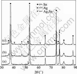
图2 室温时效不同时间后Ag/Sn偶的XRD谱
Fig.2 XRD patterns of Ag/Sn couple after ageing for different time: (a) As-deposited; (b) 1 d; (c) 10 d
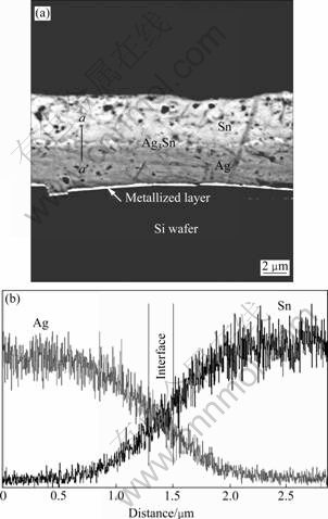
图3 室温时效10 d后Ag/Sn 偶截面背散射电子像(a)及跨界面成分线扫描(b)
Fig.3 Cross sectional backscattering SEM photograph(a) and EDX linear scanning pattern cross interface(b) of Ag/Sn couple after ageing for 10 d
一般地,元素周期表中的IB 副族贵金属原子(如Cu、Ag 和Au) 即使在室温条件下都能够在IIIA及 IVA主族金属(如In、Sn和Pb)中借助间隙扩散的方式快速扩散,并发生相互作用形成金属间化合物型的反应产物[8]。而通常电镀材料均为多晶材料,晶界扩散也会扮演重要角色。Ag在Sn中间隙、晶界扩散及Sn 在Ag 中晶界扩散是电镀偶主导的原子迁移过程,室温下两者速率(扩散系数)相当,均约为10-17 m2/s[11]。该数值比Cu(Au)/Sn系统中Cu(Au)原子间隙扩散系数小几个数量级[8],因此,在Ag/Sn界面通过Ag与 Sn原子的相互扩散形成Ag3Sn的反应速率也要低得多。同时,当在界面形成连续的Ag3Sn薄层后,阻碍Ag、Sn原子通过Ag3Sn层向对方扩散,导致Ag3Sn的生长更加缓慢。基于一元扩散控制反应动力学模型:
X2=kt (1)
式中 X为反应层厚度,m;k 为反应层长大速率常数,m2/s;t为反应时间,s。可以估算出室温Ag3Sn层的长大速率常数约为1×10-20~4×10-20 m2/s,与室温下Ag3Sn中的原子互扩散系数(3.4×10-20 m2/s)[8]相当,远小于该温度条件下Ag在Sn 中或Sn在Ag中的原子扩散系数(10-17 m2/s)。
SIMI?等[16]系统研究了不同Ag、Sn质量比(Ag、Sn层厚度比)下的气相沉积Ag/Sn偶室温界面固相反应过程,发现反应物成分的变化对反应产物的组成没有影响,即反应区中仅有Ag3Sn而无Ag4Sn。究其原因,SEN 等[11]认为,在Ag/Sn界面处Ag4Sn新相的形核更困难。但这也可能和热力学因素有关,室温Ag3Sn的形成焓数值比Ag4Sn的更大(ΔH298 K, Ag3Sn= -4.2 kJ/mol,ΔH298 K, Ag4Sn= -2.8 kJ/mol)[17],Ag3Sn形成的可能性更大。此外,根据BANDYOPADHYAY等[18]的经验规律,优先形成的反应产物(相)应是在二元系统相图上成分与最低共晶点的成分最接近的化合物相。由图1可见,Ag3Sn作为Ag/Sn系统优先形成相,也是符合这个规律的。
2.2 热处理条件下的界面反应
图4所示为热处理Ag/Sn偶的XRD谱,图5所示为不同热处理温度、时间条件下反应层的截面形貌。热处理条件下的Ag/Sn界面反应仍然只形成Ag3Sn,没有出现Ag4Sn(图4)。由图5可见,在未反应的Ag和Sn 层之间形成了一定厚度连续的Ag3Sn层,而且随热处理温度的升高反应层厚度明显增加(图5(a)~(c))。经(200 ℃,1.5 h)热处理后,绝大多数的Ag均参与反应,仅有一薄层剩余,这与图4(c)中极高的Ag3Sn衍射峰强度相对应。另外,通过比较图3和图5可以看出,Ag/Sn界面反应形成的Ag3Sn层似乎更多地存在于Ag/Sn原始界面Ag的一侧,这说明该反应的进行主要是借助于Sn通过Ag3Sn层向Ag中的扩散来进行的。也就是说,在Ag3Sn中Sn具有比Ag更大的扩散速率。尽管还没有找到Ag和Sn在Ag3Sn 中的扩散数据,但该结果与CHEN等[19]发现的在Sn-Ag-Au系统中形成Ag3Sn相时,Ag原子基本不动,而Sn原子是快速扩散原子的实验结果相符。
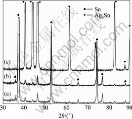
图4 经不同温度和时间热处理后Ag/Sn偶的XRD谱
Fig.4 XRD patterns of annealed Ag/Sn couples at different temperatures for various times: (a) 150 ℃, 1 h; (b) 200 ℃, 0.5 h; (c) 200 ℃, 2 h
当热处理温度升高到225 ℃(仍低于Sn的熔点(231 ℃))时,Ag/Sn偶试样已出现了明显熔化的迹象(图6)。原先反应物及反应产物层状结构的特征消失,代之以颗粒状、块状组织的不连续分布。XRD分析表明,经(225 ℃,0.5 h)热处理后的Ag/Sn偶试样中除包含反应物 Sn及产物Ag3Sn外,还有Si表面金属化Pt及其与Sn反应所形成的反应产物PtSn4相,但没有出现Ag的衍射峰(图7)。结合能谱分析可以确定图6中的球形颗粒为Ag3Sn 相(67.2% Ag, 32.8% Sn,摩尔分数),而靠近Si晶片侧白亮的块体为PtSn4 (20.0% Pt,80.0% Sn,摩尔分数) 的柱状晶。Sn(0.7% Ag,99.3% Sn,摩尔分数)分布在Ag3Sn及PtSn4颗粒(晶粒)周围。显然,在此热处理条件下,Ag/Sn偶中,Ag与Sn反应形成层状的Ag3Sn,直至Ag全部消耗完。由于(Sn+Ag3Sn)共晶温度为221 ℃,低于225 ℃的热处理温度,导致液相的形成。同时,富含Sn的液相与Pt籽晶层反应形成PtSn4柱状晶[20]。在热处理后的冷却过程中,从液相中结晶出球状的Ag3Sn和Sn的共晶组织。
2.3 反应动力学
经125~200 ℃热处理,Ag/Sn界面固相反应形成Ag3Sn层的生长动力学曲线如图8所示。反应层厚度(X)与热处理时间平方根(t1/2)的线性关系表明,Ag/Sn界面固相反应呈现抛物线型反应动力学特征,为一个扩散控制的反应过程,即该反应受反应物原子(Ag、Sn)在Ag3Sn反应区中的扩散过程控制。不同温度下的反应速率常数如图8所示。
界面固相反应速率常数(k)和热处理温度(T)的关系可用Arrhenius方程表示:

式中 k0为指前因子,m2/s;Q为反应激活能,J/mol;R为一般气体常数,8.31 J/(K?mol)。Ag/Sn界面固相反应速率常数与热处理温度倒数的关系如图9所示。在图9所示的线性关系曲线上,采用截距法和外推法得到该界面反应的激活能及指前因子分别为70.0 kJ/mol和5.0×10-8 m2/s。尽管还没有Ag/Sn二元系统界面固相反应动力学数据报道,但TAKENAKA等[21]报道Ag0.87Au0.13/Sn 三元系统界面固相反应形成Ag3Sn的激活能及指前因子分别为74.0 kJ/mol和3.6×10-8 m2/s。SU等[22]报道固态Ag与液态Sn间界面反应的激活能为70.3 kJ/mol。这些数据都与本文的实验结果十分接近。
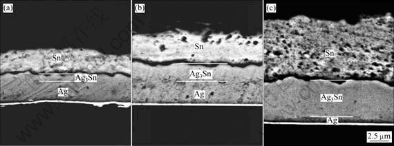
图5 经不同温度和时间热处理后Ag/Sn偶的截面背散射电子像
Fig.5 Cross-sectional backscattering SEM photographs of Ag/Sn couples annealed at different temperatures for various times: (a) 125 ℃, 8 h; (b) 150 ℃, 6 h; (c) 200 ℃, 1.5 h
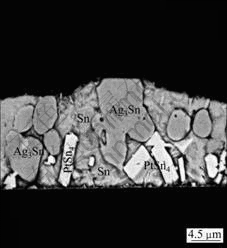
图6 经(225 ℃, 0.5 h)热处理后Ag/Sn偶截面背散射电子像
Fig.6 Cross-sectional backscattering SEM photograph of Ag/Sn couple annealed at 225 ℃ for 0.5 h
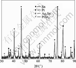
图7 经(225 ℃, 0.5 h)热处理后Ag/Sn偶的XRD谱
Fig.7 XRD pattern of Ag/Sn couple annealed at 225 ℃ for 0.5 h
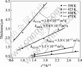
图8 Ag3Sn层的平均厚度与热处理时间的关系
Fig.8 Relationship between average thickness of Ag3Sn layer and square root of time for annealed Ag/Sn couples
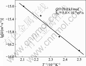
图9 Ag3Sn层生长速率常数与热处理温度的关系
Fig.9 Relationship between k values and annealing temperature for Ag3Sn layer in annealed Ag/Sn couples
3 结论
1) 在电沉积Ag/Sn偶过程中发生Ag与Sn间的界面反应,形成层状结构的Ag3Sn。反应偶在室温时效过程中,Ag3Sn层的生长缓慢。
2) 在125~200 ℃热处理过程中,反应形成的Ag3Sn层在Ag及Sn层之间均匀连续分布,随着热处理温度的提高,Ag3Sn层的生长速率明显提高。当在225 ℃热处理时,反应形成的Ag3Sn与残余的Sn之间发生共晶反应,形成液相。同时,Sn与Pt之间反应形成PtSn4,室温组织为球状Ag3Sn与柱状PtSn4颗粒(晶粒)分布于连续的Sn基体中。
3) 125~200 ℃下的Ag/Sn界面固相反应遵循抛物线型的反应动力学,受反应物原子在Ag3Sn层中的 固相扩散过程控制。反应的动力学方程为k = 5.0× 10⁻⁸ exp[70.0×10³/(RT)]。
REFERENCES
[1] KIM J S, LEE C C. Fluxless Sn-Ag bonding in vacuum using electroplated layers[J]. Mater Sci Eng A, 2007, 448: 345-350.
[2] CHAO B, CHAE S H, ZHANG X F, LU K H, IM J, HO P S. Investigation of diffusion and electromigration parameters for Cu-Sn intermetallic compounds in Pb-free solders using simulated annealing[J]. Acta Mater, 2007, 55: 2805-2814.
[3] TANG W M, HE A Q, LIU Q, IVEY D G. Fabrication and microstructures of sequentially electroplated Sn-rich Au-Sn alloy solders[J]. J Electron Mater, 2008, 27: 837-844.
[4] CHEN C M, CHEN S W. Electromigration effect upon the Sn/Ag and Sn/Ni interfacial reactions at various temperatures[J]. Acta Mater, 2002, 50: 2461-2469.
[5] LIAO C N, WEI C T. Effect of intermetallic compound formation on electrical properties of Cu/Sn interface during thermal treatment[J]. J Electron Mater, 2004, 33: 1137-1143.
[6] 祝清省, 张 黎, 王中光, 吴世丁, 尚建库. 金属间化合物Ag3Sn对Sn3.8Ag0.7Cu焊料合金拉伸性能的影响[J]. 金属学报, 2007, 43(1): 41-46.
ZHU Qing-sheng, ZHANG Li, WANG Zhong-guang, WU Shi-ding, SHANG Jian-ku. Effect of intermetallic Ag3Sn on the tensile property of Sn3.8Ag0.7Cu solder alloy[J]. Acta Metallurgica Sinica, 2007, 43(1): 41-46.
[7] LI Guo-yuan, SHI Xun-qing. Effects of bismuth on growth of intermetallic compounds in Sn-Ag-Cu Pb-free solder joints[J]. Trans Nonferrous Metals Soc China, 2006, 16(s1): 739-743.
[8] LAURILA T, VUORINEN V, KIVILAHTI J K. Interfacial reactions between lead-free solders and common base materials[J]. Mater Sci Eng R, 2005, 49: 1-60.
[9] 韩永典, 荆洪阳, 徐连勇, 郭伟杰, 王忠星. Sn-Ag-Cu无铅焊料的可靠性研究[J]. 电子与封装, 2007, 7(3): 4-6, 33.
HAN Yong-dian, JING Hong-yang, XU Lian-yong, GUO Wei-jie, WANG Zhong-xing. Study on the reliability of Sn-Ag-Cu lead-free solders[J]. Electronics & Packaging, 2007, 7(3): 4-6, 33.
[10] GALE W F, TOTEMEIER T C. Smithells metal reference book[M]. 8th ed. MA, USA: Elseiver Butterworth-Heinemann, 2004: 11-25.
[11] SEN S K, GHORAI A, BANDYOPADHYAY A K. Interfacial reactions in bimetallic Ag-Sn couples[J]. Thin Solid Films, 1987, 155: 243-253.
[12] ARAI S, AKATSUKA H, KANEKO N. Sn-Ag solder bump formation for flip-chip bonding by electroplating[J]. J Electrochem Soc, 2003, 150: C730-C734.
[13] SUZUKI K, KANO S, KAJIHARA M, KUROKAWA N, SAKAMOTO K. Reactive diffusion between Ag and Sn at solid state temperatures[J]. Mater Trans JIM, 2005, 46: 969-973.
[14] HE A, LIU Q, IVEY D G. Development of stable, non-cyanide solutions for electroplating Au-Sn alloy films[J]. J Mater Sci: Mater Electron, 2006, 17: 63-70.
[15] TANG W M, HE A Q, LIU Q, IVEY D G. Room temperature interfacial reactions in electrodeposited Au/Sn couples[J]. Acta Mater, 2008, 56: 5818-5827.
[16] SIMIC V, MARINKOVIC Z. Review: Room-temperature reactions in thin metal couples[J]. J Mater Sci, 1998, 33: 561-624.
[17] FLANDORFER H, SAEED H, LUEF C, SABBAR A, IPSER H. Interfaces in lead-free solder alloys: Enthalpy of formation of binary Ag-Sn, Cu-Sn and Ni-Sn intermetallic compounds[J]. Thermochimica Acta, 2007, 459: 34-39.
[18] BANDYOPADHYAY A K, SEN S K. A sudy of intermetallic compound formation in a copper-tin bimetallic couple[J]. J Appl Phys, 1990, 67(8): 3681-3688.
[19] CHEN S W, YEN Y W. Interfacial reactions in the Sn-Ag/Au couples[J]. J Electron Mater, 2001, 30: 1133-1137.
[20] WANG S J, LIU C Y. Coupling effect in Pt/Sn/Cu sandwich solder joint structures[J]. Acta Mater, 2007, 55: 3327-3335.
[21] TAKENAKA T, KAJIHARA M, KUROKAWA N, SAKAMOTO K. Reactive diffusion between Ag-Au alloys and Sn at solid-state temperatures[J]. Mater Sci Eng A, 2006, 427: 210-222.
[22] SU T L, TSAO L C, CHANG S Y, CHUANG T H. Morphology and growth kinetics of Ag3Sn during soldering reaction between liquid Sn and an Ag substrate[J]. J Mater Eng Performance, 2002, 11: 365-368.
收稿日期:2008-08-13;修订日期:2009-02-13
通讯作者:汤文明,教授,博士;电话:0551-2901372;E-mail: wmtang69@126.com
(编辑 李向群)

