
First large scale application of novel Si stripixel detector in real large experiment: Si VTX in PHENIX upgrade at RHIC
LI Zheng1, H. ENYO2, Y. GOTO2, J. TOJO2, Y. AKIBA, R. NOUICER,
A. L. DESHPANDE4, K. BOYLE4, V. CIANCIOLO5
1. RIKEN BNL Research Center and BNL Instrumentation Division, Upton, NY 11973-5000, USA;
2. RIKEN, Wako, Saitama 351-0198, Japan;
3. BNL, Chemistry Department, Upton, NY 11973-5000, USA;
4. Stony Brook University, Department of Physics and Astronomy, Stony Brook, NY 11794, USA;
5. Oak Ridge National Laboratory, Oak Ridge, TN 37831, USA;
Received 10 April 2006; accepted 25 April 2006
Abstract: 2D position sensitive, single-sided Si stripixel detector was selected as the one of the two main components of the Si vertex tracker (Si SVX) in the upgraded PHENIX detector at RHIC (relativistic heavy ion collider) in Brookhaven National Laboratory (BNL). This is the first large scale application of the novel Si stripixel detector in a real large experiment after many years of research and development at BNL. The first and second prototype fabrication runs of the SVX stripixel detectors were carried out successfully in BNL’s Si detector development and processing Lab. The processing of these stripixel detectors is similar to that for the standard single-sided strip detectors: one-sided processing, single implant for the pixel (strip) electrodes, etc. The only additional processing step is the double metal process, a technology that is simple and well matured by many Si detector processing industries and labs, including BNL. The laser and beam tests on those prototype detectors show the 2D position sensitivity and good position resolution in both X and U coordinates (about 25 ?m for 80 ?m pitch). For the mass production of 400 sensors needed for the Si SVX, the processing technology has been successfully transferred to the industrial: Hamamatsu Photonics (HPK). HPK has produced a pre-production run of stripixel sensors with the full PHENIX SVX specification on 150 mm diameter wafers. The laser tests on these pre-production wafers show good signal to noise ratio (about 20∶1).
Key words: Si strip detector; Si stripixel detector; vertex detector; 2D Si detector; 2D position sensitivity; AC coupling
1 Introduction
The PHENIX detector at RHIC (Relativistic Heavy Ion Collider) in Brookhaven National Laboratory (BNL) has been running successfully since 2000 with good physics results [1]. However, the current PHENIX detector at RHIC is inadequately equipped to fully exploit the opportunities of exploring physics provided by RHIC. For PHENIX upgrade, a Si vertex tracker (SVX) has been proposed to add tracking capabilities to the central arms of the PHENIX experiment [2]. Fig.1 shows the illustration of the PHENIX Upgrade, with the SVX in the center of the detector system.
One of the two main components of SVX detector is the Si stripixel detector system. Novel Si stripixel detectors have been developed during the last five years in BNL [3-6]. Stripixel detector is a single-sided, 2-dimensional (2D) sensitive detector that is simpler for detector fabrication and signal processing than the conventional double-sided strip detector. Fig.2 shows the stripixel detector concept. Each pixel in the detector is divided into Y and X (or U if there is a stereo angle(? 90?) between the two coordinates) sub-pixels. The two sub-pixels (X and Y) of each pixel are interleaved in such way that the charge cloud (including the expansion caused by diffusion) is generated by hit of a particle coves both X and Y sub-pixels, generating a current/charge signal on both sub-pixels. The X sub-pixels are connected by X strips and the Y sub-pixels are connected by Y strips. Since a hit of a particle will generate a signal in both X and Y sub-pixels, and therefore in both X and Y strips, we have a 2D position sensitive detector with only one-sided processing in both detector fabrication and signal treatment. The only addition to the fabrication process is a two-metal process
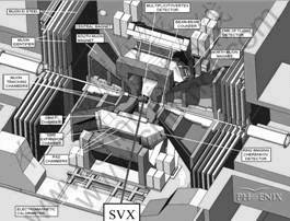
Fig.1 Upgraded PHENIX detector at RHIC with SVX in the middle
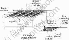
Fig.2 Stripixel detector concept with interleaved spiral shaped X and Y sub-pixels
that is used to separate X and Y strips. However, we have recently made design and fabrication of 2D, single-side processed Si stripixel detectors with only a single metal process for PHENIX calorimeter [7].
In this paper, testing results on sensors from prototype detector runs at BNL and from the preproduction run of the contracting industry for mass production are shown.
2 Prototype fabrication runs at BNL
The schematic of the first prototype Si strip detector for SVX in PHENIX Upgrade is shown in Fig.3.
Detectors were made on 100 mm diameter n-type Si
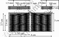
Fig.3 Schematic diagram of sensor layout of first prototype Si stripixel detector for PHENIX SVX
wafers, with a resistivity of 4-6 kW?cm. The thicknesses of these wafers were 250 mm and 400 mm, and they were processed at BNL. The chip size is 3 cm by 6 cm, and the detector is divided into two identical halves. In the left half, there are 384 Y strips with 80 mm pitch and bonding pads for readout on the left side; and there are 384 U (or X) strips with 80 mm pitch and bonding pads for readout in the middle of the wafer. The stereo angle between Y and U strips is about 4.6?. The right half is a mirror copy of the left one with respect to the middle line of the detector chip.
Fig.4 shows the cross section of the detector after the photo lithography on the second metal. The first Al is the metal contacts for all pixels, including Y and U (or X) sub-pixels. All Y-strips are routed out by the first Al as well. All U-strips are routed out by the second Al. The crossing of the first and second Al strips are separated by an insulating layer polyimide, with exception of the via contacts on the U sub-pixels.
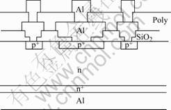
Fig.4 Cross section view of double metal layout of Si strip detector via contacts on U sub-pixels
Fig.5 shows the photograph of a Si stripixel detector in the first prototype batch of PHENIX SVX. Y strips are routed out to the left to bonding pads (not shown), and U strips are clearly seen with a small angle (4.6°) with respect to the horizontal. The contact vias to X sub-pixels (X-cells in the figure) are also visible.
Fig.6 shows the beta-source and beam (KEK) test results on the stripixel detectors from the first batch of
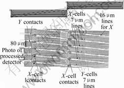
Fig.5 Photograph of first batch prototype Si strip detectors: Y strips and X (U) strips
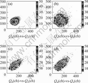
Fig.6 Correlation between Y and U coordinates for β-source and KEK beam as determined by the first prototype stripixel detectors for PHENIX SVX: (a) β-source; (b) Beam, θinc=0?; (c) Beam, θinc=15?; (d) Beam, θinc=30?
PHENIX SVX. These figures plot the correlation of Y and U coordinates measure by the 2D stripixel detectors. Position resolution of about 25 ?m have been obtained for both X and U coordinates, which is just about the pitch 40/ ?m.
?m.
It is clear that the best correlation has been obtained by the beta-source tests. As for beam tests, there is a dependence on the incident beam angle. These asymmetries may be caused by the un-even charge sharing between Y and U sub-pixels due to the large separation between the two sub-pixels (13 ?m pitch between Y and U sub-pixels (7 ?m line width, and 6 ?m gap)).
To correct this charge sharing asymmetry problem, a second batch has been produced at BNL in 2004 after a design change that reduces the Y and U sub-pixels pitch from 13 ?m to 8 ?m (5 ?m line width, and 3 ?m gap). This change indeed improves the charge sharing significantly. But there is a trade-off between the small Y and U sub-pixels pitch and the inter-strip capacitance: small Y and U sub-pixels pitch will result in longer effective strip length and therefore larger inter-strip capacitance. The 8 ?m Y and U sub-pixels pitch value seems to be an optimum compromise.
3 Pre-production fabrication run at Hamamatsu photonics
In 2005, the stripixel technology developed for PHENIX SVX, including the mask design and processing technology, has been transferred successfully from BNL to the detector fabrication industry, the Hamamatsu photonics, Japan (HPK), for mass production. By the middle of 2005, HPK has produced a pre-production batch of Si stripixel detectors on 6” diameter wafers with thickness of 625 ?m, and resistivity >10 kW?cm. As shown in Fig.7, for ease of readout electronics arrangements, the bonding pads for both Y and U strips are moved to the top and bottom of the detector chip, with readout routing lines perpendicular to the strips. This routing arrangement, however, does not require an additional metal layer in the processing, i.e. it is still a double-metal process. Fig.8 shows the photo of a HPK wafer with 3 PHENIX SVX Si stripixel detectors. Each detector has an active area of about 3 cm×6 cm, with strip length of 3 cm. The leakage current of these detectors are about on average of 0.4 nA/strip, and inter-strip capacitance of about 10 pF/strip.
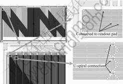
Fig.7 Design layout of HPK pre-production batch of Si stripixel detectors for PHENIX SVX
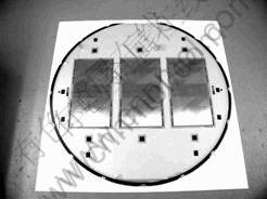
Fig.8 Photo of 6” wafer with 3 Si stripixel detectors for PHENIX SVX, processed by HPK
In the fall of 2005, IR laser tests have been performed on these HPK detectors in Oak Ridge National Lab. Fig.9 clearly shows the 2D position sensitivity of the detector with laser induced signal in both X and U strips.
Signal to noise ratio (S/N) measurements shown better than 20∶1 S/N on these HPK Si stripixel detectors for PHENIX SVX. This value is expected taking into account the charge sharing between the Y and U strips.
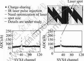
Fig.9 IR laser inducing signals in X and U strips of a HPK Si stripixel detector for PHENIX SVX
The mass production of 400 sensors will soon start at HPK. A QA program has been set up here at BNL to pick out 200 good sensors needed for PHENIX SVX, and this task will be completed in 2007. The full SVX detector system will be assembled and installed in 2008-2009 in RHIC at BNL.
4 Development of new AC coupled stripixel detectors at BNL
As the mass production is near its start at HPK, the PHENIX SVX has been planed to AC couple those Si stripixel detectors (which are DC coupling after detector processing) into the readout electronics. The reason for this is that as the radiation level goes up at PHENIX, the detector leakage current may go up to a level too high to saturate the SVX4 readout chip, thus disable the detector. Although by cooling the detector to sub-zero temperatures, the detector leakage currents can be significantly lowered; there are some real advantages of operating the detector system at or near room temperature (25 ℃). Also, for most existing detector systems with strip detectors, they are AC-coupled strip detectors with related readout electronics [8-10]. A fall-back plan with internal, intergraded AC couple stripixel detector for PHENIX SVX has been developed at BNL at the end of 2005.
The geometry of AC coupled stripixel detectors is similar to that of the HPK pre-production DC coupled stripixel detectors, except on the left and right sides of the detector chip, there are bias resistors connected together to a bias line, as shown in Fig.10. Each bias resistor, with a designed value of 1 MW, is connected to a strip (either Y or U strip). The processing of AC coupled stripixel detectors requires a triple-metal technology: the 1st metal is used to supply DC bias to the detector, the second metal is used to AC coupling each strip, and the 3rd metal is used to bridging the crossings of Y and U
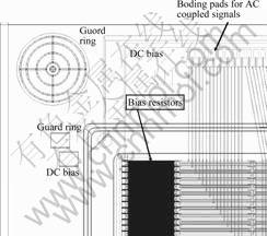
Fig.10 Top left corner of AC coupled stripixel detector for PHENIX SVX with bias resistors and bonding pads
strips, and to route the AC coupled readout lines to bonding pads on the top and bottom of the detector chip.
The 1st and 2nd metals are separated by the 1st layer of insulator (polyimide or CVD SiO2), which is also used as the coupling capacitor, with a designed value of 130 pF. The pixel pattern for Y and U sub-pixels are exactly the same for the 1st and 2nd metals. As shown in Fig.11, at each crossing point of Y and U strips, Y sup-pixels are connected horizontally by ion implant (boron ions here through 100 nm of SiO2 for p+) for DC biasing (we note here that by using an ion implant here for Y connection, we can effectively use a single metal process for a DC coupled stripixel detector, as it has been implemented in Ref.7), and by the 3rd metal for AC coupling; and U sub-pixels are connected diagonally by the 1st metal for DC biasing, and by the 2nd metal for AC coupling. There is an additional layer of insulator used to separate the 2nd and 3rd metals. The main
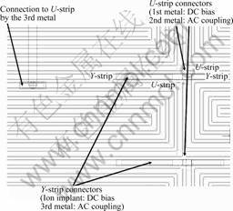
Fig.11 Design schematics of X and U strip connections and readout line for AC coupled stripixel detector for PHENIX SVX
processing steps are as the follows: 1) p+ pixels formation (boron ion-implant); 2) via opening for metal contact; 3) 1st metal formation (for DC biasing); 4) bias resistor formation (polysilicon or WNx deposition and etching); 5) 1st insulator layer formation (for AC coupling); 6) 2nd metal formation (AC coupling); 7) 2nd insulator layer formation (isolate 2nd and 3rd metals); and 8) 3rd metal formation (bridging and routing the readout lines). Processing steps 4), 7) and 8) are additional for AC coupled Si stripixel detectors.
The mask set design for AC coupled Si stripixel detectors is completed now, and we will soon start the first prototype batch processing of AC coupled stripixel detectors for PHENI SVX. By the end of summer 2006, we should be able to perform the initial tests on these detectors, such as the leakage current, coupling capacitance, and inter-strip capacitance.
5 Summary
Over the last 5 years, the development of novel Si stripixel detector has been carried at BNL. As their first large scale application, stripixel detector will be fabricated for PHENI SVX at RHIC in BNL. The successful transfer of stripixel technology ensures that large quantity of stripixel detectors can be made outside of BNL by a major detector industry. New development on AC coupled Si stripixel detectors has shown it possible to internally AC couple the stripixel detectors with AC coupling technology commonly used for standard AC coupled strip detectors. Processing of the first prototype AC coupled Si stripixel will soon begin and new results on AC coupled stripixel detectors will be obtained in fall 2006.
References
[1] Adcox K. PHENIX Collaboration. PHENIX detector overview[J]. Nucl Instr and Meth A, 2003, 499: 469-479.
[2] Ciancolo V. PHENIX SVX, silicon vertex upgrade for PHENIX, PHENIX Internal Note an180, 2003.
[3] Li Z. Novel silicon stripixel detector: Concept, simulation, design, and fabrication [J]. Nucl Instr & Meth A, 2004, 518: 738-753.
[4] Li Z, En’yo H, Goto T, Radeka V, Chen W, Elliott D, Kawabata T, Togawa M, Saito N, Rykov V, Tanida K, Tojo J. Novel silicon stripixel detector for PHENIX upgrade [J]. Nucl Instr and Meth A, 2004, 518: 300-304.
[5] Li Z, En’yo H, Goto T, Radeka V, Chen W, Elliott D, Kawabata T, Togawa M, Saito N, Rykov V, Tanida K, Tojo J. Development of 2 prototype of novel silicon stripixel detector for phenix upgrade [J]. Nucl Instr and Meth A, 2004, 535: 404-409.
[6] Tojo J, Aoki K, En’yo H, Fukao Y, Goto Y, Heuser J M, Li Z, Ohnishi H, Okada H, Radeka V, Rykov V L, Saito N, Sakuma F, Sekimoto M, Tanida K, Togawa M, Watanabe Y. Development of a novel silicon stripixel detector for RHIC-PHENIX detector upgrade [J]. IEEE Trans Nucl Sci, 2004, 51: 2337.
[7] Kistenev E, Li Z, Merkine M, Seto R, Sukhanov A, Vrba V. Silicon sensors for the forward calorimeters for the PHENIX experiment at RHIC [A]. IEEE Nucl Sci Symp[C].Puerto Rico: IEEE Trans Nucl Sci, 2005.
[8] Chabaud V, et al. Beam test results from a prototype for the delphi microvertex detector[J]. Nucl Instr and Meth A, 1990, 292: 75.
[9] CMS Technical Proposal. CERN/LHCC/94-38, 1994.
[10] ATLAS Technical Proposal. CERN/LHCC 94-43, 1994.
(Edited by YANG Hua)
Foundation item: Project(DE-Ac02-98CH10886) supported in part by the US Department of Energy
Corresponding author: LI Zheng; Tel: +001-631-344-7604; Fax: +001-631-344-5773; E-mail: zhengl@bnl.gov

