J. Cent. South Univ. Technol. (2011) 18: 125-132
DOI: 10.1007/s11771-011-0669-7

Design of 1 kbit antifuse one time programmable memory IP using dual program voltage
JIN Li-yan(金丽妍), JANG Ji-Hye, KIM Du-Hwi, HA Pan-Bong, KIM Young-Hee
Department of Electronic Engineering, Changwon National University, 9 Sarim-Dong,
Changwon 641-773, Korea
? Central South University Press and Springer-Verlag Berlin Heidelberg 2011
Abstract: A 1 kbit antifuse one time programmable (OTP) memory IP, which is one of the non-volatile memory IPs, was designed and used for power management integrated circuits (ICs). A conventional antifuse OTP cell using a single positive program voltage (VPP) has a problem when applying a higher voltage than the breakdown voltage of the thin gate oxides and at the same time, securing the reliability of medium voltage (VM) devices that are thick gate transistors. A new antifuse OTP cell using a dual program voltage was proposed to prevent the possibility for failures in a qualification test or the yield drop. For the newly proposed cell, a stable sensing is secured from the post-program resistances of several ten thousand ohms or below due to the voltage higher than the hard breakdown voltage applied to the terminals of the antifuse. The layout size of the designed 1 kbit antifuse OTP memory IP with Dongbu HiTek’s 0.18 ?m Bipolar-CMOS-DMOS (BCD) process is 567.9 μm×205.135 ?m and the post-program resistance of an antifuse is predicted to be several ten thousand ohms.
Key words: one time programmable memory IP; antifuse; hard breakdown; dual program voltage; post-program resistance
1 Introduction
Non-volatile memory (NVM) IP is generally applied to perform analog trimming, security, key encryption, and embedded memory repair function in SoC chips such as power management IC, LCD driver IC and CMOS image sensor [1]. Among NVMs, one time programmable (OTP) memory is widely used since it consists of low-area and does not require optional processes [2].
There are efuse-type memories and antifuse-type memories as OTP memories. An efuse-type memory uses an efuse as its memory element. Since the process technology of the efuse is shrunk down, the silicide material deposited on the poly-Si is changed to tungsten silicide [3], titanium silicide [4], cobalt silicide [5], copper silicide [6], and nickel silicide [7]. There are a single ended bit line (BL) sensing scheme and a double ended BL sensing scheme as BL sensing schemes [8]. Recently, the efuse OTP memories are used widely as repair fuses replacing laser fuses of a large storage capacity memory [9]. An antifuse-type OTP memory is smaller than an efuse-type counterpart in size and has an advantage of being performed byte by byte in the program and read mode. The OTP memory of antifuse type is programmed by shortening electrically via the breakdown mechanism when a high voltage is applied to a MOS transistor with a thin gate oxide.
As the thickness of a thin gate oxide falls down to 40 ? or smaller, post program resistances due to the soft breakdown [10] tend to distribute widely up to several million ohms. Thus, it is necessary to apply a voltage higher than the hard breakdown voltage (BV) to the thin gate oxide to reduce the post-program resistance down to several ten thousand ohms. However, a conventional antifuse OTP cell uses a single positive program voltage (VPP) and is subject to restriction when raising VPP because of the reliability of medium voltage (VM) devices. Thus, there is a good possibility for failures in a qualification test or a yield drop from failures in sensing if the post-program resistances due to the soft breakdown are above several million ohms.
In this work, we propose a new antifuse OTP cell using a dual program voltage to prevent the possibility for failures in a qualification test or the yield drop. The dual program voltage scheme means applying high VPP (=8 V) and VNN (=-6 V) to the terminals of the antifuse. For the newly proposed cell, a stable sensing is secured from the post-program resistances of several ten thousand ohms or below due to the voltage higher than the hard breakdown voltage applied to the terminals of the antifuse. A 1 kbit OTP memory IP is designed with Dongbu HiTek’s 0.18 ?m Bipolar-CMOS-DMOS (BCD) process. The layout size is 567.9 μm×205.135 ?m.
2 Trends in design of antifuse-type OTP memories
An antifuse-type OTP cell to be programmed by applying a high voltage to a MOS transistor with a thin gate oxide is classified into a single port OTP cell sharing its read and write port [11-13] and a dual port OTP memory cell with its separate read and write port [14]. As shown in Fig.1, there are a three-transistor (3T) cell, a two-transistor (2T) cell, and a 1.5-transistor (1.5T) cell as a single port OTP cell.
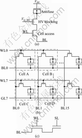
Fig.1 OTP memory cells: (a) 3T OTP cell; (b) 2T OTP cell; (c) 1.5T OTP cell
As shown in Fig.1(a), a 3T cell consists of an antifuse-type NMOS capacitor with its thin gate oxide, a high-voltage (HV) blocking transistor, and an access transistor. If the gate voltage of the thin-oxide NMOS capacitor that is an antifuse is applied with VPP (=6 V), the gate node of the HV blocking transistor with VG-BT, the selected word line (WL) with supply voltage (VDD), and BL with 0 V in the program mode, the NMOS capacitor is shortened electrically since it is broken down with an applied high voltage of more than the break-down voltage of its gate oxide. In the 3T OTP cell, WL is 0 V and BL is 0 V for the programmed cell in the program mode. Since an additional HV blocking transistor is required to reduce the leakage current by the gate-induced drain leakage (GIDL) effect in the case that VPP is applied to the cell access transistor directly, there is the possible disadvantage that the layout area of a cell may be large.
On the contrary, in the 2T cell shown in Fig.1(b), the gate oxide is broken down by applying WL with VPP/2 (=3.5 V), GL (gate line) with VPP (=7 V), and BL with 0 V for the selected cell in the program mode. The gate oxide is not broken down in the case of the non- programmed cell in the program mode if BL is floating when WL is applied with 0 V and GL with VPP/2. Since all GLs are applied with VDD (=1.8 V) and the selected WL with VDD in the read mode, a datum is outputted through the current sensing circuit. Also, since the non-selected WLs are applied with 0 V, the OTP cell is separated from BL. Since GL is applied with VPP or VPP/2 in the program mode and with VDD in the read mode, three power supplies of VPP, VPP/2 and VDD are required. Furthermore, there is a disadvantage that the layout area may be larger from requiring an additional gate bias switch circuit since an OTP cell array grows greater than eight rows if the store capacity of OTP memory increases. Also, an additional bias voltage (VBias) circuit is required since a datum is output by comparing the pull-down current through BL with the pull-up current of the NMOS transistor which is biased to VBias using a current sensing circuit.
Fig.1(c) shows a Kilopass’s antifuse OTP cell. The 1.5T OTP cell consists of an NMOS access transistor and a half transistor of antifuse. The cell size is the smallest among the antifuse OTP cells.
Fig.2 shows a conventional two-port antifuse OTP cell. The two-port antifuse OTP cell consists of a PMOS antifuse with thin gate oxide, and a write port and a read port transistor with thick gate oxide. The size of the write port transistor grows larger to obtain a sufficient programming current and the resistance through the
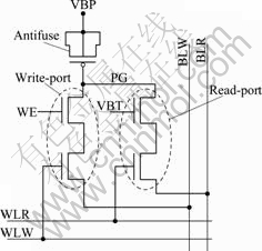
Fig.2 Dual port OTP memory cell
writing path is reduced by making the metal width of write bit line (BLW) wider. Also, the width of the read port transistor is set to its minimum to reduce its read current and the parasitic capacitance of read bit line (BLR) is minimized using a minimum BLR wiring.
Fig.3(a) shows a PMOS antifuse circuit used in an antifuse cell. The source, drain, and N-well body node are connected to the same node. The antifuse is biased as shown in Fig.3(a). The thickness of a thin gate oxide based on Dongbu HiTek’s 0.18 ?m BCD process is 38 ?. Fig.3(b) shows an I-V curve after a program voltage of 10 V is applied. One of five samples fails during programming. Fig.4 shows I-V curves that ensemble the 30 samples after the same program voltage of 11 V is applied and it can be seen that all the samples are successful upon programming. Their post-program resistances are all under several ten thousand ohms. As shown in the measurement results of Fig.3 and Fig.4, there needs a driving circuit applying a higher voltage
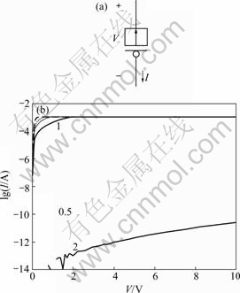
Fig.3 PMOS antifuse circuit (a) and I-V curve (b)
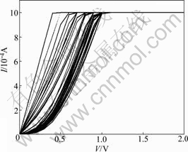
Fig.4 I-V curves after applying program voltage of 11 V
than the hard breakdown voltage between the terminals of the antifuse.
3 Circuit design
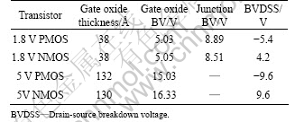
In this work, we propose a dual-port antifuse OTP cell which can be programmed by a dual program voltage such that a high voltage of more than the hard break-down voltage is applied between the terminals of an antifuse. Table 1 shows the key parameters of the transistors used in the proposed OTP memory cell: gate oxide thickness, gate oxide breakdown voltage, junction breakdown voltage, and BVDSS. The breakdown voltages are all measured at 10 nA.
Table 1 Key parameters of transistors used in proposed OTP memory cell
As shown in Fig.5(a), the proposed antifuse OTP memory cell consists of a 1.8 V low voltage (LV) PMOS antifuse (MP0), a switching transistor (MP1) transferring VPP (=8 V) or VDD (=1.8 V) through positive data line (PDL) in the program mode and a read-out transistor (MN0) transferring information about the antifuse to BL in the read mode. The gate of the PMOS antifuse is connected to negative data line (NDL) and is supplied with VNN (=-6 V) or 0 V. In Fig.5(a), MN0 and MP1 are shown where MV transistors are thick gate oxides. In the proposed OTP memory cell, a LV PMOS transistor is used with no requirement of deep N-well as an antifuse to reduce the layout size. Fig.5(b) shows its layout image. Since the terminals of the PMOS antifuse are applied with a higher voltage than the hard breakdown voltage of its thin gate oxide for the designed OTP cell, the post-program resistance of the antifuse is under several thousand ohms. For Dongbu HiTek’s 0.18 ?m BCD process, a voltage of 11 V or above should be applied to the terminals of the antifuse to break it since the hard breakdown voltage of the 1.8 V PMOS antifuse is 11 V, as shown in Fig.4.
The OTP memory has two operational modes: program and read. Table 2 shows bias voltage conditions at various nodes for various operation modes of a OTP cell. In the program mode, VPP is driven by an external voltage of 8 V. Selected write word line bar (WWLb) is kept at 0 V and non-selected WWLb is kept at VPP. Also, read word line (RWL) is always applied with 0 V in the

Fig.5 Circuit (a) and its layout image (b) of designed OTP cell (VSS―Voltage of virtual ground)
Table 2 Bias voltage conditions for various operation modes of OTP cell node
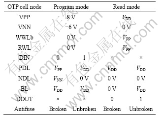
program mode. In case that DIN is applied with ‘0’, PDL and NDL are applied with VPP and VNN, hence the antifuse breaks and shortens electrically. In case that DIN is ‘1’, PDL and NDL are applied with VDD. At 0 V, the antifuse does not break and is in the open state electrically. For the designed OTP memory, a programmed cell means that DIN is applied with a logic ‘0’ and a non-programmed cell means that DIN is applied with a logic ‘1’. On the other hand, RWL is activated to VDD after BL is pre-charged to VDD in the read mode. For the programmed cell, since a current path is supplied to NDL through a shortened PMOS antifuse, BL is discharged to 0 V and DOUT outputs a logic value of ‘0’. In comparison with the non-programmed cell, since a current path is blocked through an open PMOS antifuse, BL is kept at a pre-charged voltage of VDD and DOUT outputs a logic value of ‘1’, as shown in Table 2.
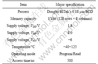
Major specifications of the designed asynchronous 1 kbit OTP memory are shown in Table 3. The cell array of 1 kilo bits is arranged as 128 rows × 8 columns. The supply voltages used are: logic supply voltage VDD (=1.8 V) and dual program voltage VPP (=8 V) and VNN (=-6 V).
Table 3 Major specifications of asynchronous OTP memory of 1 kilo bits
As shown in Fig.6, the designed 1 kbit OTP memory consists of a OTP memory cell array of 128 rows × 8 columns, a WL driving circuit selecting one of 128 WLs by decoding the address bus A[6:0], a WD (write data) driver, a BL S/A (bit-line sense amplifier) and a control logic that supplies internal control signals. This is suitable for both the program and the read mode. This is based on the control signals (RD and program). The WD drives an input datum DIN[7:0] to OTP cells through data lines PDL[7:0] and NDL[7:0] in the program mode. The BL S/A outputs a digital datum through DOUT[7:0] by sensing a datum coming from BL[7:0]. The bits vary according to the programmed states.
Fig.7(a) shows a timing diagram for the asynchronous OTP memory in the program mode. When PGM is activated highly after the address bus A[6:0] and an input byte are applied, the byte of the selected OTP memory cells is programmed with DIN[7:0]. During the programming time, VPP and VNN should be kept at 8 V and -6 V. Fig.7(b) shows a timing diagram for the asynchronous OTP memory in the read mode. When READ is activated highly after the address bus A[6:0] is applied by keeping VPP and VNN at VDD and VSS, the byte of the selected OTP memory cells is read out through DOUT[7:0] in an access time tAC. In this state, PGM should remain low and DIN[7:0] is in the “don’t-care” state. A separate I/O method is used, which means that the input and output ports are separately used.
Referring to Fig.8(a), the WL driving circuit makes WLEN_PGM a logic ‘1’ in entering the program mode. Only one WWLb selected by decoding the row address A[6:0] is driven to 0 V and the others are kept to VPP at
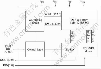
Fig.6 Block diagram of 1 kbit OTP memory

Fig.7 Timing diagram in program (a) and in read mode (b)
this state. The WL driving circuit makes WLENb_RD a logic ‘1’ in entering the program mode. Only selected RWL is driven by VDD. The PDL driving circuit in Fig.8(b) supplies VDD or VPP in the program mode. PDL is driven to 0 V if input data (DIN) have a logic value of ‘1’, and to VPP if DIN has a logic value of ‘0’. Also, PDL drives VDD since the signal PGM_EN has a logic value of ‘1’ in the read mode. The NDL driving circuit in Fig.8(c) supplies VSS or VNN in the program mode. NDL is driven to VSS if DIN has a logic value of ‘1’, and to VNN if DIN has a logic value of ‘0’. Also, NDL drives VSS since the signal PGM_EN has a logic value of ‘0’ in the read mode.
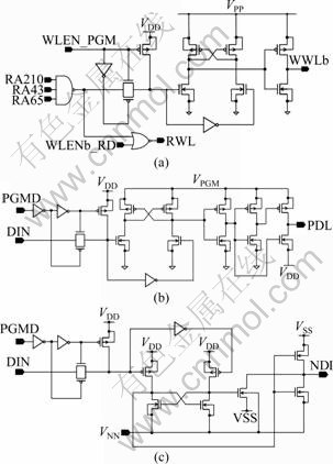
Fig.8 WL driving circuit (a), PDL driving circuit (b), and NDL driving circuit (c)
For the designed OTP memory, both programming and reading are done byte by byte. Fig.9 shows a BL sense amplifier (S/A) of clocked inverter type. As shown in Fig.9, the BL S/A consists of a pull-up transistor (MP0) with low impedance, a pull-up transistor (MP1) with high impedance and a D latch with clocked inverters. In the read mode, BL is pre-charged to VDD by a short pulse of PRECHARGE before RWL is activated. If RWL is activated, BL connected to a programmed cell with a logic value of ‘1’ is kept at VDD while BL is discharged to 0 V for the programmed cell with a logic value of ‘0’ since the antifuse becomes short. If sense amplifier enable bar (SAENb) is activated to 0 V after a datum to be read is transferred to BL sufficiently, a BL S/A of clocked inverter type senses either VDD or 0 V and outputs the read datum to DOUT [15].
4 Simulation results
We designed an asynchronous 1 kbit antifuse OTP memory IP with Dongbu HiTek’s 0.18 ?m BCD process. Fig.10 shows a function simulation result in the program mode, where VPP and VNN are set up before PGM is applied. Since selected WWLb is activated lowly by PGM, and PDL and NDL are supplied with 8 V and -6 V, the hard breakdown occurs at the antifuse and programming can be done there. The simulation conditions of Fig.10 are as follows: VDD 1.62 V, temperature 25 °C, and slow model parameters. The simulation in Fig.10(a) is done assuming that the antifuse resistance is set up at 100 kΩ. As shown in Fig.10(a), the voltage between the terminals of the antifuse, VAF, is 12.5 V. We can see that this is above the hard breakdown voltage of 11 V in Fig.4. Fig.11 shows a timing diagram for RD from the programmed OTP memory cell, and PRECHARGE and SAENb from the control logic in Fig.6. If RD is applied, BL is pre-charged to VDD by a short pulse of PRECHARGE. As RWL is activated after BL is pre-charged, the BL S/A senses and outputs the read datum to DOUT if a datum of the OTP cell is transferred to BL sufficiently by SAENb. The simulation of Fig.11 is done under the following conditions: VDD 1.62 V, temperature 125 °C, and slow model parameters. The access time tAC is 413 ns in the worst case.
Fig.12 shows a layout image of the designed 1 kbit OTP memory IP with the 0.18 ?m BCD process. The layout size is 567.9 ?m × 205.135 ?m.
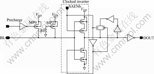
Fig.9 BL sense amplifier of clocked inverter type
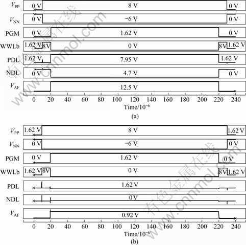
Fig.10 Simulation results in program mode: (a) DIN=‘0’; (b) DIN=‘1’
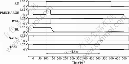
Fig.11 Simulation result in read mode

Fig.12 Layout image of designed 1 kbit OTP memory
5 Conclusions
1) The 1 kbit antifuse OTP memory IP is designed with Dongbu HiTek’s 0.18 ?m BCD process.
2) The 1 kbit antifuse OTP IP is designed by applying to thin gate oxides with dual program voltage which is higher than the hard breakdown voltage. The antifuse to be programmed is applied with dual power of VPP (=8 V) and VNN (=-6 V), and the non-programmed one with VDD (=1.8 V). Thus, the antifuse which is applied with a voltage higher than 12 V undergoes hard breakdown.
3) The post-program resistance is predicted to be several ten thousand ohms.
Acknowledgement
This research is financially supported by Changwon National University in 2009-2010.
References
[1] ITO H, NAMEKAWA T. Pure CMOS one-time programmable memory using gate-Ox anti-fuse [C]// SZAJDA K. Proceedings of the CICC 2004 Conference. Florida: Institute of Electrical & Electronics Engineers Inc, 2004: 469-472.
[2] KOTHANDARAMAN C. Electrically programmable fuse (eFUSE) using electromigration in silicides [J]. IEEE Electron Device Letters, 2002, 23(9): 523-525.
[3] FELLNER J, BOESMUELLER P, REITER H. Lifetime study for a poly fuse in a 0.35 mm polycide CMOS process [C]// Proceedings of IEEE the 43rd Annual International Reliability Physics Symposium. San Jose: Reliability Physics Symposium, 2005: 446-449.
[4] ALAVI M, BOHR M, HICKS J, DENHAM M, CASSENS A, DOUGLAS D, TSAI M C. A PROM element based on silicide agglomeration of poly fuses in a CMOS logic process [C]// IEEE Electron Devices Society. Proceedings of IEEE Electron Devices Meeting. Washington: Institute of Electrical & Electronics Engineers Inc, 1997: 855-858.
[5] KPTHANDARAMAN C, IYER S K, IYER S S. Electrically programmable fuse (efuse) using electromigration in silicides [J]. IEEE Electron Device Letters, 2002, 23(9): 523-525.
[6] UEDA T, TAKAOKA H, HAMADA M, KOBAYASHI Y, ONO A. A novel Cu electrical fuse structure and blowing scheme utilizing crack-assisted mode for 90-45 nm-node and beyond [C]// Proceedings of Symposium on VLSI Technology. Hawaii: Symposia on VLSI Technology & Circuits, 2006: 138-139.
[7] SAFRAN J, LESLIE A, FREDEMAN G, KOTHANDARAMAN C, CESTERO A, CHEN X, RAJEEVAKUMAR R, KIM D K, LI Y Z, MOY D, ROBSON N, KIRIHATA T, IYER S. A compact efuse programmable array memory for SOI CMOS [C]// NATARAJAN S. Proceedings of Symposium on VLSI Circuits. Kyoto: Emerging Memory Technologies Inc, 2007: 72-73.
[8] ROBSON N, SAFRAN J, KOTHANDARAMAN C, CESTERO A, CHEN X, RAJEEVAKUMAR R, LESLIE A, MOY D, KIRIHATA T, IYER S. Electrically programmable fuse (efuse): From memory redundancy autonomic chips [C]// MECHLER J T. Proceedings of IEEE Custom Integrated Circuits Conference. San Jose: Institute of Electrical and Electronics Engineers Inc, 2007: 799-804.
[9] LIM K N, KANG S S, CHOI J H, JOO J H, LEE Y S, LEE J S, CHO S I, RYU B G. Bit line coupling scheme and electrical fuse circuit for reliable operation of high density DRAM [C]// MOTOMURA M. Proceedings of Symposium on VLSI Circuits. Kyoto: IEEE Service Center Single Publication Sales Unit, 2001: 33-34.
[10] DEPAS M. Soft Breakdown of Ultra-Thin Gate Oxide Layers [J]. IEEE Transactions on Electron Devices, 2004, 43(9): 1499-1504.
[11] CHOI J S, WEE J K, CHO H Y, KIM P J, OH J K, LEE C H, CHUNG J Y, KIM S J, YANG W. Antifuse EPROM circuit for field programmable DRAM [C]// WUORINEN J H. Proceedings of IEEE International Solid-State Circuits Conference. San Francisco: IEEE Standards Office, 2000: 406-407.
[12] CHA H K, YUN I H, KIM J B, SO B C, CHUN K H, NAM I K, LEE K R. A 32-KB standard CMOS antifuse one-time programmable ROM embedded in a 16-bit microcontroller [J]. IEEE Journal of Solid-State Circuits, 2006, 41(9): 2115-2124.
[13] BARSATAN R, MAN T Y, CHAN M S. A zero mask one-time programmable memory array for RFID applications [C]// Proceedings of IEEE International Symposium on Circuits and Systems. Island of Kos: Institute of Electrical and Electronics Engineers, 2006: 975-978.
[14] MATSUFUJI K, NAMEKAWA T, NAKANO H, ITO H, WADA O, OTSUKA N. A 65 nm pure CMOS one-time programmable memory using a two-port antifuse cell implemented in a matrix structure [C]// Proceedings of IEEE Asian Solid-State Circuit Conference. Jeju: IEEE Solid-State Circuits Society, 2007: 212-215.
[15] LEE J H, KANG M C, JIN L Y, JANG J H, HA P B, KIM Y H. Design of a asynchronous eFuse one-time programmable memory IP of 1 Kilo bits based on a logic process [J]. Journal of Korea Institute of Maritime Information and Communication Sciences, 2009, 13(7): 1371-1378.
(Edited by YANG Bing)
Foundation item: Work supported by the Second Stage of Brain Korea 21 Projects
Received date: 2010-01-20; Accepted date: 2010-05-20
Corresponding author: KIM Young-Hee, Professor, PhD; Tel: 82-55-285-1023; E-mail: youngkim@changwon.ac.kr