Trans. Nonferrous Met. Soc. China 22(2012) 2736-2741
Effect of KOH treatment on structural and photovoltaic properties of ZnO nanorod arrays
ZHOU Yi, LI Dang, HUANG Yan, HE Wen-hong, XIAO Bin, LI Hong
School of Chemistry and Biological Engineering, Changsha University of Science and Technology, Changsha 410114, China
Received 27 September 2011; accepted 22 December 2011
Abstract: ZnO nanorod arrays (NRs) were synthesized on the fluorine-doped SnO2 transparent conductive glass (FTO) by a simple chemical bath deposition (CBD) method combined with alkali-etched method in potassium hydroxide (KOH) solution. X-ray diffraction (XRD), scanning electron microscopy (SEM) and current―voltage (I―V) curve were used to characterize the structure, morphologies and optoelectronic properties. The results demonstrated that ZnO NRs had wurtzite structures, the morphologies and photovoltaic properties of ZnO NRs were closely related to the concentration of KOH and etching time, well-aligned and uniformly distributed ZnO NRs were obtained after etching with 0.1 mol/L KOH for 1 h. ZnO NRs treated by KOH had been proved to have superior photovoltaic properties compared with high density ZnO NRs. When using ZnO NRs etched with 0.1 mol/L KOH for 1 h as the anode of solar cell, the conversion efficiency, short circuit current and open circuit voltage, compared with the unetched ZnO NRs, increased by 0.71%, 2.79 mA and 0.03 V, respectively.
Key words: ZnO nanorod arrays; SnO2 transparent conductive glass; alkali etching; structural properties photovoltaic properties; solar cells
1 Introduction
As an important II-VI semiconductor, ZnO has attracted great interests owing to its unique properties, such as a wide band gap (3.37 eV), a large exciton binding energy (60 meV), high electrochemical and thermal stability, transparency, biocompatibility, acoustic characteristics and excellently electronic properties. It has been widely used in solar cell [1,2], chemical sensors [3], varistors [4], surface acoustic wave device [5], photonic crystals [6], photodiodes [7] and so on. In particular, one-dimensional (1D) ZnO NRs have been applied to dye sensitized solar cells (DSSC) because of their specific optoelectronic properties [8]. As we know, the photoanode plays an important role in determining the electron diffusion coefficient [9], the dye absorption surface area and photon-to-charge carrier efficiency [10]. At present, mesoporous nanoparticles are used as photoanodes because of their larger inner surface, but the electron transport is slower due to the multi-trapping events. One way of addressing this problem is to introduce nanorod arrays to the photoanode. The ZnO NRs provide direct path from the point of photogeneration electron to the conducing substrate and greatly enhance their surface area, leading to improved light harvesting and overall efficiency [11]. In addition, ZnO NRs have advantage in that nanorods can be easily synthesized using a hydrothermal method [12].
Until now, different methods to synthesize ZnO NRs have been used, such as metal organic chemical vapor deposition (MOCVD) [13], template-based method [14], laser ablation [15], spray pyrolysis technique [16], and solution methods [17]. Compared with those methods, the chemical solution deposition method (CBD) can be controlled easily under low temperature, and no sophisticated equipment is required [18]. Now just a little work has focused on tuning the array size of ZnO NRs [19], and the effects of KOH treatment on the morphologies and photovoltaic properties of ZnO NRs have been reported rarely.
Therefore, in this article the authors reported the two-step synthesis of ZnO NRs by a chemical bath deposition method followed by alkali-etching in KOH solution. The size and the surface area of ZnO NRs can be well tuned by varying the concentration and etching time. Eventually, the influence of this KOH treatment on the photoelectric properties of ZnO NRs is investigated by studying photocurrent―voltage (I―V) characteristics of the DSSC.
2 Experimental
2.1 Preparation process
High density ZnO NRs used in this work were grown on FTO coated glass substrates by CBD method. The FTO-coated glass substrates were first cleaned in the ultrasonic bath with acetone, ethanol and deionized water to remove adsorbed dust and surface contamination. Then, ZnO seed layer was fabricated on the substrates by a dip-coating method. The precursor aqueous solution for the preparation of ZnO NRs was composed of 0.1mol/L Zn(NO3)2 and (CH2)6N4 in a 1:1 molar ratio. The pH value of the solution was adjusted to 9.0 by the addition of ammonia. The precursor solution (60 mL) was then transferred to a Teflon-sealed autoclave comprising substrates precoated with a ZnO seed layer. The reaction was run at 95 °C for 6 h to synthesize ZnO nanorod film. After deposition, the samples were cleaned with deionized water several times and allowed to dry in air. Finally, the resulting films were immersed into 0.05, 0.1, 0.2 mol/L KOH for 0.5, 1 and 2 h, respectively.
2.2 Construction of dye-sensitized solar cell
The obtained ZnO nanorod electrodes were dipped in a N3 solution (0.5 mmol/L in dry ethanol solution) for 12 h. The counter Pt-electrode was obtained by coating with a drop of H2PtCl6 solution (5 mmol/L in isopropanol solution) on FTO and heated at 300 °C for 15 min. The dye-covered ZnO electrode and Pt-counter electrode were assembled into a sandwich type cell. The electrolyte solution composed of 0.5 mol/L KI, 0.05 mol/L I2 in acetonitrile was introduced to the gap between the counter and working electrodes by the capillary force. Then, the DSSC cell was obtained.
2.3 Characterization
The X-ray diffraction (XRD) patterns were recorded on an X-ray diffraction system (XRD, SEMENS D5000). The morphology was observed by a scanning electron microscope (SEM, JEOL JSM°C 6700F).
The current―voltage (I―V) characteristics were measured with a computer-controlled digital source meter (Keithley, model 2400) under illumination with a Newport solar simulator (AM1.5, 100 mW/cm2).
3 Results and discussion
3.1 Morphology and microstructure
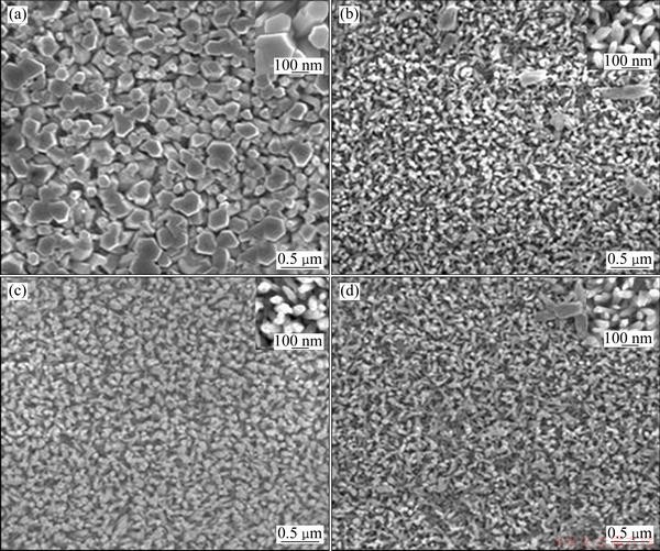
Figure 1 shows the SEM images of unetched and ZnO NRs etched by KOH with different concentrations for 1 h. The growth temperature and time of high density ZnO NRs were 95 °C and 6 h, respectively. It can be seen that the morphology of as-grown ZnO NRs is closely related to the KOH concentration. The SEM image of unetched ZnO NRs is shown in Fig. 1(a). It can be seen that the arrays consist of dense ZnO NRs with different diameters, and the average diameter is about 200 nm. The size of the ZnO NRs is varied by changing the concentration of the KOH. As shown in Fig. 1(b), the average diameter of ZnO NRs is about 50 nm. Though the diameter decreased, the ZnO NRs were still arranged densely after etching at a low concentration of the KOH (0.05 mol/L). Figure 1(c) shows that ZnO NRs were vertically well-aligned and uniformly distributed on the FTO substrate after etching by 0.1 mol/L KOH, and the average diameter was about 30 nm. However, for samples under higher KOH concentration, sparse ZnO NRs with local defects were obtained, which could be seen from Fig. 1(d).
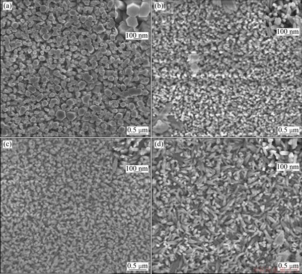
To investigate the effect of the etching time on the morphology and aspect area of ZnO NRs, a series of experiments were performed by varying the etching time of 0.1 mol/L KOH but keeping other parameters constant. Figure 2 shows the SEM images of unetched and KOH-etched ZnO NRs with different time. It can be seen that the morphology of as-grown ZnO NRs is closely related to the etching time. The diameters of ZnO NRs decreased after etching by KOH, and within certain etching time range (0.5h to 2h), the density of the ZnO NRs decreases with increasing the etching time. Because ZnO could react with KOH, the diameters decreased after etching by KOH. Furthermore, increasing the etching time is beneficial for sufficient reaction, which would lead to a decrease in the arranged density of ZnO NRs. And these can be represented by the following reaction [20]:
ZnO+2OH-→ ZnO22-+H2O (1)
The SEM image of untreated ZnO NRs is shown in Fig. 2(a). It can be seen that the arrays consist of dense ZnO NRs with different diameters, and the average diameter is about 200 nm. With the increase in the etching time while the concentration of KOH was kept at 0.1 mol/L, the density and diameters of zinc oxide nanorods also decreased (Figs. 2(b)-(d)). From Fig. 2(b), we can see that the ZnO NRs treated in 0.1 mol/L KOH solution for 0.5 h have relatively uniform nanorod structures, the impurities on the ZnO NRs may be ZnO clumps which were not cleaned up. Although the average diameter decreased (about 30 nm), the ZnO NRs were arranged densely. And as shown in Fig. 2(c), when the treating time increased to 1 h, ZnO NRs with a hexagonal wurtzite structure were vertically well-aligned and uniformly distributed on the FTO substrate. Due to the fact that the polar faces of ZnO nanorods were dissolved while the nonpolar ZnO crystals were relatively steady in KOH solution [19], no remarkable change on average diameter was observed compared with Fig. 2(b), but the interface between nanorods increased as sufficient reaction, which is beneficial to increasing the surface area of ZnO NRs. Figure 2(d) shows the SEM image of ZnO NRs etched in 0.1 mol/L KOH solution for 2 h. When ZnO NRs reacted with KOH for a long time, the orientation of the ZnO NRs is not so good and the nanorods have a slant away from the vertical, as shown in Fig. 2(d).
From Fig. 1 and Fig. 2, it can be concluded that the concentration and etching time of KOH play key roles in ZnO NRs. The morphology of the ZnO NRs etched by 0.1 mol/L KOH solution for 1 h is better than the unetched ZnO NRs or ZnO NRs etched for 0.5 h and 2 h.

Fig. 1 SEM images of ZnO NR arrays (a) and ZnO NR arrays etched by KOH with concentrations of 0.05 mol/L (b), 0.1 mol/L (c) and 0.2 mol/L (d)

Fig. 2 SEM images of ZnO NRs (a) and ZnO NRs etched by 0.1 mol/L KOH for time of 0.5 h (b), 1 h (c) and 2 h (d)
3.2 XRD patterns
Figure 3 shows the XRD patterns of the as-grown ZnO NRs grown on FTO substrate. All diffraction peaks are consistent with the wurtzite structure, which can be indexed to a standard spectrum of JCPDS (No. 36―1451). The squares denote peaks attributed to SnO2 (26.11, 33.89, 37.83, 51.56 61.72 and 65.45°, JCPDS 41―1445) from the FTO substrate. No XRD peaks except those of ZnO and SnO2 appear in the XRD data of unetched and KOH-etched ZnO NRs, indicating that only ZnO NRs are formed. When the ZnO NRs were etched by 0.1 mol/L KOH solution, the intensities of the diffraction peaks corresponding to the ZnO NRs shown in Figs. 3(b), (c) and (d) had no obvious difference in comparison with those of ZnO NRs shown in Fig. 3(a), which indicates that the crystal form of ZnO NRs has no significant change.

Fig. 3 XRD patterns of unetched ZnO films (a) and ZnO films etched by 0.1 mol/L KOH for time of 0.5 h (b), 1 h (c) and 2 h (d)
3.3 Application of ZnO NRs in DSSC
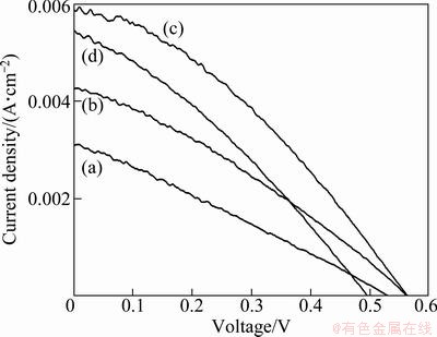
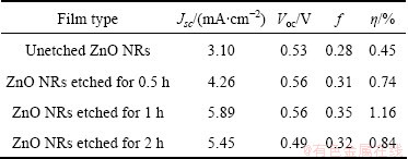
Figure 4 compares the I―V characteristics of the dye-sensitized solar cell based on ZnO NRs unetched and etched by 0.1 mol/L KOH solution with different time. The corresponding values are summarized in Table 1, which demonstrates the photoelectrochemical characteristics such as current density at short circuit, the voltage at open circuit (Voc), fill factor (f), and the efficiency of power conversion (η) in different samples. From Table 1, it is observed that the photoelectron- chemical characteristics of the DSSC-based untreated ZnO NRs were very low. However, these characteristics increased with the increase in etching time and remained stable in 0.5-1 h. And the cell efficiency decreased at the etching time of 2 h. When using ZnO NRs etched by 0.1 mol/L KOH for 1h as the anode of the dye-sensitized solar cell, the conversion efficiency (η), short circuit current (Jsc) and open circuit voltage (Voc), compared with the unetched ZnO NRs, improved by 0.71%, 2.79 mA and 0.03 V, respectively. As the ZnO NRs could provide direct path from the point of photogeneration electron to the conducing substrate and greatly enhance their surface area, leading to improved light harvesting and overall efficiency [10]. Compared with the solar cell based on ZnO NRs unetched and etched for 0.5 h, the photoelectrochemical characteristics of ZnO NRs etched for 1 h increased and the enhancement of η was attributed to the strong effect of the increase of Jsc as the the Voc and f increased slightly. This demonstrates that the increased surface area provided by etching the dense ZnO NRs enhanced the total amount of dye in the array films, thus the etched arrays had advantages over unetched arrays in light-harvesting efficiencies. And the surface area of ZnO NRs etched by 0.1mol/L KOH for 1 h was larger than that treated for 0.5 h, which could also be seen from the SEM images in Fig. 2. The solar cell efficiency decreased when the ZnO NRs was etched for 2 h. This may be correlated with the disordered structure of ZnO NRs and the loss of ZnO, which was caused by the reaction with KOH for a longer time.

Fig. 4 Current―voltage characteristics of dye-sensitized solar cell based on unetched ZnO NRs (a) and ZnO NRs etched by 0.1 mol/L KOH for time of 0.5 h (b), 1 h (c) and 2 h (d)
Table 1 Photovoltaic parameters of unetched ZnO NRs and ZnO NRs etched by 0.1 mol/L KOH for different time

4 Conclusions
1) ZnO NRs were synthesized using KOH etching on FTO substrate. The effects of KOH concentration and etching time on ZnO NRs morphology were investigated systematically. It is possible to control the morphology of ZnO NRs on the substrate by adjusting the KOH concentration and etching time.
2) The current―voltage characterizations on DSSCs suggest that the conversion efficiencies were improved by increasing the surface area and providing a direct path from the point of photogeneration electron to the conducing substrate with ZnO NRs.
References
[1] JEONG W J, KIM S K, PARK G C. Preparation and characteristic of ZnO thin film with high and low resistivity for an application of solar cell [J]. Thin Solid Films, 2006, 506-507: 180-183.
[2] ATSUSHI T, AKIRA O, TAKEYOSHI O, MAKOTO O,TAKAYUKI M, MASATOMO S, KEITA O, SHIGEFUSA F C, SYUNROU F, YUSABUROU S, HIDEO O, HZDEOMI K, MASASHI K. Repeated temperature modulation epitaxy for p-type doping and light-emitting diode based on ZnO [J]. Nature Materials, 2005, 4(1): 42-46.
[3] COMINI E, BARATTO C, FAGLIA G, FERRONI M, SBERVEGLIERI G. Single crystal ZnO nanowires as optical and conductometric chemical sensor [J]. Journal of Physics D, 2007, 40(23): 7255-7259.
[4] PRADHAN B, BATABYAL S K, PAL A J. Vertically aligned ZnO nanowire arrays in Rose Bengal-based dye-sensitized solar cells [J]. Solar Energy Materials and Solar Cells, 2007, 91(9): 769-773.
[5] CHU Sheng-yuan, CHEN Te-yi, WATER W. Deposition of preferred-orientation ZnO films on the ceramic substrates and its application for surface acoustic wave filters [J]. Journal of Vacuum Science and Technology A, 2004, 22(4):1087-1092.
[6] KEE C S, KO D K, LEE J. Photonic band gaps of two-dimensional ZnO nanorod photonic crystals [J]. Journal of Physics D, 2005, 38(21): 3850-3853.
[7] ZHANG Zu-wei, HU Cheng-guo, XI Yi. Nano devices based on ZnO nanobelt [J]. Materials Review, 2007, 21(z1): 113-116.
[8] WEI Su-feng, JIANG Qing, LIAN Jian-she. Synthesis and characteristics of large-scale ZnO rods by wet chemical method [J]. Transactions of Nonferrous Metals Society of China, 2008, 18(5): 1089-1093.
[9] BAUER C, BOSCHLOO G, MUKHTAR E, HAGFELDT A. Electron injection and recombination in Ru(dcbpy)2(NCS)2 sensitized nanostructured ZnO [J]. Journal of Physical Chemistry B, 2001, 105(24): 5585-5588.
[10] QUINTANA M, EDVINSSON T, HAGFELDT A, BOSCHLOO G. Comparison of dye-sensitized ZnO and TiO2 solar cells: Studies of charge transport and carrier lifetime [J]. Journal of Physical Chemistry C, 2007, 111(2): 1035-1041.
[11] BAXTER J B, AYDIL E S. Dye-sensitized solar cells based on semiconductor morphologies with ZnO nanowires [J]. Solar Energy Materials and Solar Cells, 2006, 90(5): 607-622.
[12] SONG J, LIM S. Effect of seed layer on the growth of ZnO nanorods [J]. Journal of Physical Chemistry C, 2007, 111(2): 596-600.
[13] CHEN Yi-feng, TANG Mo-tang, ZHANG Bao-ping, YANG Sheng-hai. Crystal morphologies of ZnO obtained by oxidizing zinc vapor [J]. Transactions of Nonferrous Metals Society of China, 2004, 14(3): 504-508.
[14] LI Y, MENG G W, ZHANG L D. Ordered semiconductor ZnO nanowire arrays and their photoluminescence properties [J]. Applied Physics Letters, 2000, 76(15): 2011-2013.
[15] DUAN Xiang-feng, LIEBER C M. General synthesis of compound semiconductor nanowires [J]. Advanced Materials, 2000, 12(4): 298-302.
[16] ROZATI S M, AKESTE S. Influence of substrate temperature on the structure of ZnO:Al thin films [J]. Crystal Resesch and Technology, 2008, 43(3): 273-275.
[17] HOLMES J D, JOHNSTON K P, DOTY R C, KORGEL B A. Control of thickness and orientation of solution-grown silicon nanowires [J]. Science, 2000, 287(5457): 1471-1473.
[18] LI Qing-wei, BIAN Ji-ming, SUN Jing-chang, WANG Jing-wei, LUO Ying-min, SUN Kai-tong, YU Dong-qi. Controllable growth of well-aligned ZnO nanorod arrays by low-temperature wet chemical bath deposition method [J].Applied Surface Science, 2010, 256(6): 1698.
[19] YANG H Y, LEE S H, KIM T W. Effect of zinc nitrate concentration on the structural and the optical properties of ZnO nanostructures [J]. Applied Surface Science, 2010, 256(20): 6117-6120.
[20] SHE Guang-wei, ZHANG Xiao-hong, SHI Wen-sheng, FAN Xia, LEE Chun-sing, LEE Shuit-tong, LIU Chang-hong. Controlled synthesis of oriented single-crystal ZnO nanotube arrays on transparent conductive substrates [J]. Applied Physics Letters, 2008, 92(5): 053111.
KOH处理对ZnO纳米棒阵列结构及光电性能的影响
周 艺,李 荡,黄 燕,何文红,肖 斌,李 宏
长沙理工大学 化学与生物工程学院,长沙 410114
摘 要:采用简单的化学沉积结合KOH碱刻蚀的方法,在导电玻璃(FTO)上生长ZnO纳米棒阵列(ZnO NRs)。用X射线衍射(XRD)、扫描电子显微镜(SEM)、电流―电压(I―V)曲线对所得样品的晶型、形貌及光电性能进行测试,结果表明:ZnO NRs呈纤铅矿型;ZnO NRs的形貌及光电性能与KOH的浓度及刻蚀时间密切相关,经0.1 mol/L KOH刻蚀1 h后可得到排列高度有序且分布均匀的ZnO NRs;KOH刻蚀后的ZnO NRs与未刻蚀前高密度的ZnO NRs相比,其光学性能得到提高。0.1 mol/L KOH刻蚀1 h的ZnO NRs作为太阳能电池的光阳极,其光电转换效率、短路电流、开路电压较未刻蚀的ZnO NRs分别提高了0.71%、2.79 mA和0.03 V。
关键词:ZnO纳米阵列;SnO2导电玻璃;碱刻蚀;结构性能;光电性能;太阳能电池
(Edited by YANG Hua)
Foundation item: Project (21171027) supported by the National Natural Science Foundation of China; Project (K1001020-11) supported by the Science and Technology Key Project of Changsha City, China; Project ([2010]70) supported by Science and Technology Innovative Research Team in Higher Educational Institutions of Hunan Province, China
Corresponding author: ZHOU Yi; Tel: +86-13755001202; E-mail: zhouyihn@163.com
DOI: 10.1016/S1003-6326(11)61526-4