Recent progress of CERN 39-cryogenic tracking detectors collaboration
J.H?rk?nen
Helsinki Institute of Physics, CERN/EP, CH-1211 Geneva, Switzerland
Received 10 April 2006; accepted 25 April 2006
Abstract: Significant progress was made by the CERN RD39 collaboration in the development of super radiation-hard cryogenic silicon detectors for applications in experiments at LHC, in particular after its future luminosity upgrade. The detailed modeling shows that the electric field in irradiated silicon detectors can easily be manipulated by the filling state of two deep defect levels at cryogenic temperature. Advanced radiation hard detectors using charge or current injection and the current injected detectors(CID) were developed by RD39. The results show that CID detectors can be operated at the temperature of 100-200 K with much improved charge collection efficiency(CCE) as compared with RT operation. Future studies are developing ultra-hard cryogenic silicon detectors for the LHC upgrade, where the radiation hardness is required up to 1016 neq/cm2, at which trapping will limit the charge collection depth to the range of 20 to 50 ?m regardless of the depletion depth. The key of our approach is to use freeze-out trapping to affect CCE.
Key words: cryogenic, silicon, particle detector, trapping
1 Introduction
CERN RD39 collaboration is working for development of super-radiation hard cryogenic Si detectors for applications for LHC experiments and their future upgrades. Radiation hardness up to 1016 neq/cm2 is required in the future HEP experiments[1]. The most important measure of the detector radiation hardness is the charge collection efficiency (CCE), which is affected by both the detector sensitive volume (depletion depth) and charge trapping by radiation-induced trapping centers. However, 1016 neq/cm2 fluence is well beyond the radiation tolerance of even the most advanced semiconductor detectors fabricated by commonly adopted technologies: 1) the full depletion voltage will be in the thousands of volts for a 300 ?m thick Si detector operated at or near room temperature(RT); 2) at this radiation load, the charge carrier trapping will limit the charge collection depth to an effective range of 20 to 30 ?m regardless of depletion depth. In order to improve the detector overall CCE, one has to solve two above problems simultaneously[2].
The CERN RD39 collaboration has constructed transient current technique(TCT) and charge collection efficiency(CCE) set-ups with temperature range from 2 K to 300 K (LHe-TCT). The TCT is a method to measure trapping and electric field parameters in irradiated detector. The interest in the extension of the temperature range down to helium temperatures is not only in the super LHC tracker detectors, but also in the basic understanding of heavily radiation-damaged silicon.
RD39 collaboration has developed advanced detectors based on charge or current injection. In a current injection detector(CID), the electric field is controlled by injected current, which is limited by the space charge, yielding a nearly uniform electric field in the detector, independent of the radiation fluence. The unique advantage of CID is that it can operate in a fully depleted mode irrespective of its thickness. With CID concept, it is additionally possible to increase the absolute value of the colleted charge when the concentration of active trapping centers is reduced by cooling down to cryogenic temperatures.
2 Liquid helium transient current technique (LHe-TCT) measurement setup
The transient current technique method for detector characterization is developed by Ioffe Institute (St.Petersburg, Russia) and Brookhaven National Laboratory (Brookhaven, USA) [3-5]. By the TCT measurement, it is possible to determine the full depletion voltage, effective trapping time and the sign of the space charge in the bulk. The TCT measurement is based on the detection of the dominant type of charge carrier, electron or hole, which drifts across the whole detector thickness after being triggered by a photon. This is achieved by illuminating the front (p+ implant) or back (n+ implant) side of the detector with a 660 nm diode laser, the light penetrates a few microns into the silicon. The absorbed photons create electron-hole pairs close to the device surface.
If the front-side of the device is illuminated (p+ contact), the gathered current is coming from the electrons if the backside is illuminated, the hole current is measured. This is due to the fact that when the front-side of the detector is illuminated, the holes are gathered to the p+-electrode so fast that the signal is damped by the rise-time of the data acquisition (DAQ) electronics, and therefore the measured signal is mainly coming from the electrons that travel a longer distance through the silicon bulk. Correspondingly, when the back-side of the detector is illuminated, mainly the hole current is measured, because the electrons are gathered rapidly on their closest electrode on the back side.
Depending on the conductivity type of the bulk, the electric field, i.e. the collecting junction, is either on the front side or the back side of the detector. When measured from the front side, if the junction is on the front side, a descending electron transient current is measured. If the junction is on the back side, i.e. the bulk has inverted, an ascending electron transient current is measured. Similarly, when measured from the backside, an ascending hole transient current is measured if the junction is on the front side. If the bulk has inverted, the holes drift to the junction on the back side, and then a descending hole transient current is seen.
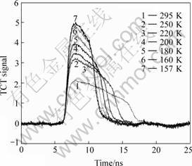
The LHe-TCT setup was constructed in 2005 in the premises of CERN��s cryolab. First measurement at the low temperatures were performed in December 2005. An example of measurement is illustrated in Fig.1.
It can be seen from Fig.1 that the current transient becomes faster with temperature decreasing, i.e. the charge collection time is shorter. This illustrates the importance of the cooling if the bunch-crossing interval is reduced to 10 ns as proposed to take place during the LHC luminosity upgrade[1]. Furthermore, it is qualitatively obvious that the trapping of the charge within the defect concentration limited time constant is reduced if the charge is collected in shorter time.

Fig.1 Example of temperature dependent TCT measurement (Sample is non-irradiated standard Fz-Si detector biased at full depletion)
3 Current injected detector(CID)
The simplest structure of current injected detector (CID) with self-limited injected current is a symmetric p+-n-p+ or p+-p-p+ structure. It can be made of n-type or p-type silicon both. The initial doping in these devices will be compensated by deep levels, thus the resistivity of the material is not an important parameter. The deep levels can be intentionally introduced during the detector processing by introducing impurities or simplied by irradiation[6].
The CID operation principle is based on the physics of current flow in heavily doped insulators[7]. In symmetric structure under applied bias, the holes are injected into the detector volume from one of the p+ contacts. The injected holes are trapped to the deep levels in the detector bulk. This affects the space charge density and the electric field distribution. The steady state density of the trapped charge is distributed in such a way that the electric field at the injecting contact (Einj) goes down, and at a certain value of the injection current, it becomes close to zero. Under these conditions, the increase of the injection current density Jinj will be limited by the low value of Einj and remains stable. This mode is known as a space-charge- limited current(SCLC) mode observed earlier in insulators.
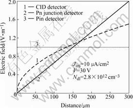
The solution of the continuity and poisson equations using the Shockley�CRead�CHall statistics as the carriers trapped by deep levels gives the charge density distribution. The solution is obtained for a deep level with activation energy Et-EV=0.48 eV and concentration (Ndl) 2.8��1012 cm-3. The resulting electric field is proportional to the square root of the distance from the injecting contact as shown in Fig.2.

Fig.2 Electric field distribution of CID detector
The electric field has a maximum at the contact opposite to the injecting contact. The magnitude of the electric field only depends on the detector thickness(d) and the bias voltage(V). Since the E(x) profile is independent on the material properties, no sensitivity to radiation influence is expected. The calculated E(x) distribution at V=30 V (Fig.2) well illustrates that the detector is fully depleted. Without charge injection, the depth of the space charge region would be only 120 ��m determined by the concentra- tion of deep levels.
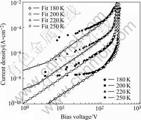
CIDs have been processed on Fz-Si wafers with high resistivity of 5-7 k��?cm and thick of 350-400 ��m. The detector active area is 10 or 25 mm2. Additionally, a set of irradiated regular p+-n-n+ detectors processed from standard high resistivity silicon and magnetic Czochralski silicon (Fz-Si 5-7 k��?cm, MCz-Si 1 k��?cm)[8]. In order to reveal the possible influence of the detector processing on the CID operation, the devices were selected from the batches processed at different institutes, i.e. Brookhaven National Laboratory (USA), Research Institute of Material Science and Technology (Russia), Helsinki Institute of Physics (Finland). The detectors were irradiated by neutrons in the range of 5��1014-3��1015 neq/cm2. The detector current voltage (IV) characteristics were measured at dry nitrogen at the temperature of 180-250 K. IV characteristics of p+-n-p+ current injected detector irradiated with a fluence of 1��1015 neq/cm2 are shown in Fig.3.
Three parts can be distinguished in the IV curve. First, nearly linear regions with a slope close to one in the range of low bias (3-40 V), then, in the medium bias valtage range of 40-200 V. After the current of the medium bias region increases sharply. It should be noted that the increasing current sharply is not breakdown. The similar IV curves were observed for regular p+-n-n+ irradiated detectors. The reproducibility of the IV characteristics was checked in the measurement with bias voltage increasing and decreasing, and no hysteresis was observed.
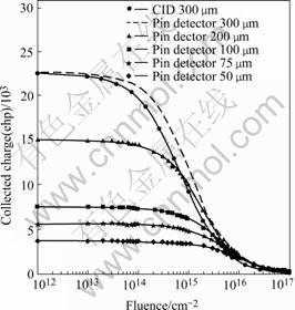
The CCE of a current injected detector has been simulated and compared with standard detectors of different thicknesses. The simulation is shown in Fig.4.

Fig.3 IV characteristics and fittings to physical model of 1��1015 cm-2 irradiated CID at different temperatures

Fig.4 Simulated CCE of CID detectors and standard detectors of different thicknesses
The simulation does not take into account the evolution of the Vfd with respect of irradiation fluence. The decrease of the CCE in this simulation is only due to trapping, i.e. degradation of the charge carrier lifetime. The minimum ionizing particles are assumed to generate 22500 electron hole pairs in 300 ��m thick silicon.
4 Conclusions
1) The most important criterion for radiation hard detectors is absolute amplitude of the signal or the value of collected charge. In super-LHC, the tracking sensors close to the interaction point will be subjected to the maximum fluence as high as 1��1016 neq/cm2 in 10 years. With such extremely high radiation level, the CCE of silicon detectors is limited not only by the electric field distribution in the detector, but also increasingly by the trapping of free carriers by shallow trap centers.
2) The electrical modeling of the sensor was verified by measurements on a series of device structures up to irradiation fluences of 5��1015 neq/cm2. Our results show that, at the very high fluences above 1��1015 neq/cm2, the symmetric p+�Ci�Cp+ structure is superior to the standard radiation hard structure p+�Ci�Cn+, and that the CCE has a broad maximum around 130 K[9].
3) The mostly optimistic estimation of the signal for standard PIN detectors irradiated to 1��1016 neq/cm2 is 1400 electrons for a fully depleted device. However, due to the extensively elevated full depletion voltage, the collected charge is in reality only 230 electrons at 300 V bias. In case of thin detectors, the full depletion is maintained and 50 ��m thick PIN device is operated at 300 V bias, the collected charge of 1 MIP will be 1370 electrons. The charge collected in 300 ��m thick CID at 1��1016 neq/cm2 and 300V bias is 1360 electrons, which is close to fully depleted PIN device. The basic property of CID is to operate in fully depleted mode irrespective of its thickness and it is unique advantage.
4) Additionally, we find that CID sensors can be operated at the temperature of 100-200 K with much improved CCE as compared to room temperature or moderate low temperatures (e.g. -100 ��) of current tracker systems. The advantage of such detector starts in the range of 100 V bias, which is significantly lower than that of the regular junction detector irradiated more than 1��1015 neq/cm2. The increase of charge collection depth is achieved without compromising the detector thickness, which potentially increases the processing related costs and lowers the signal to noise ratio.
5) Additionally, the cryogenic operation of Si detectors offers some obvious advantages, e.g. no leakage current (low electrical power from HV supply), fast charge transit (higher mobilities) and readout electronics becomes faster with less noise.
6) Future studies are developing ultra-radhard cryogenic silicon detectors for LHC upgrade. We are convinced that our approach to freeze-out detrimental trapping centers and the control of their electrical activity via charge injection is feasible for the future very high luminosity collide applications.
References
[1] GIANOTTI F, et al. hep-ph/0204087, 2002.
[2] H?RK?NEN J, et al. Recent results from the CERN RD39 collaboration on super-radiation hard cryogenic silicon detectors for LHC and LHC upgrade [J]. Nuclear Instruments and Methods in Physics Research A, 2004, A535 : 384-388.
[3] EREMIN V, LI Z. Determination of the fermi-level position for neutron irradiated high resistivity silicon detectors and materials using the transient charge technique (TChT) [J]. IEEE Transactions on Nuclear Science, 1994, 41(6): 1907-1912.
[4] EREMIN V, LI Z, ILJASHENKO I. Trapping induced Neff and electrical field transformation at different temperatures in neutron irradiated high resistivity silicon detectors [J]. Nuclear Instruments and Methods in Physics Research A, 1995, 360: 458-462.
[5] EREMIN V, et al. Development of transient current and charge techniques for the measurement of effective net concentration of ionized charges (Neff) in the space charge region of p-n junction detectors [J]. Nuclear Instruments and Methods in Physics Research A, 1996, 372: 388-398.
[6] EREMIN V, et al. Current injected detectors(CID)��a new approach for detector operation in very high radiation environment [J]. Nuclear Science Symposium Conference Record, 2004, 3: 2003-2006.
[7] LAMPERT M, MARK P. Current Injection in Solids [M]. NY, London: Academic Press, 1970.
[8] H?RK?NEN J, et al. Processing of microstrip detectors on czochralski grown high resistivity silicon substrates [J]. Nuclear Instruments and Methods in Physics Research A, 2003, 514: 173-179.
[9] BORER K, et al. Charge collection efficiency of irradiated silicon detectors operated at cryogenic temperatures [J]. Nuclear Instruments and Methods in Physics Research A, 2000, 440: 5.
(Edited by LI Yan-hong)
Corresponding author: J. H?rk?nen; Tel: +41-22-7671534; Fax: +41-22-7673600; E-mail: jaakko.haerkoenen@cern.ch