·ЕөзәПҪр»Ҝ№ӨТХФЪAA6082 Al-Mg-SiВБәПҪрұнГжНҝёІЧФИу»¬Мј»ҜОпІгөДРОіЙәНұнХч
АҙФҙЖЪҝҜЈәЦР№ъУРЙ«ҪрКфС§ұЁ(УўОД°ж)2016ДкөЪ12ЖЪ
ВЫОДЧчХЯЈәWang-Chih Chen Hung-Mao Lin Jun-Yen UAN
ОДХВТіВлЈә3205 - 3218
№ШјьҙКЈәAl-Mg-SiВБәПҪрЈ»ұнГжёДРФЈ»·ЕөзәПҪр»ҜЈ»ЧФИ󻬣»ИИҪвМјЈ»ҝ№өзҙЕёЙИЕРФДЬ
Key wordsЈәAl-Mg-Si aluminum alloy; surface modification; electrical discharge alloying; self-lubricating; pyrolytic carbon; electromagnetic interference shielding
ХӘ ТӘЈәІЙУГ·ЕөзәПҪр»Ҝ№ӨТХ¶ФAA6082 Al-Mg-SiКұР§УІ»ҜВБәПҪрҪшРРұнГжёДРФЎЈФЪ·ЕөзәПҪр»Ҝ№эіМЦРЈ¬ЧчОӘ№ӨЧчТәөДГәУНИИҪвіЙМјЈ¬ҙУ¶шРОіЙёҪЧЕУЪәПҪрұнГжөДЧФИу»¬Мј»ҜОпІгЎЈTEMҪб№ыұнГчЈ¬әПҪрұнГжРОіЙөДЧФИу»¬Мј»ҜОпІгОӘУЙМј»ҜОпәНКҜД«ЧйіЙөД¶аПаІДБПЎЈТтҙЛЈ¬ҫӯ·ЕөзәПҪр»ҜёДРФВБәПҪрөДДҰЛрВКј«РЎЈ¬ФјОӘ2ЎБ10-4 mg/mЈ¬¶шВБәПҪр»щМеөДДҘЛрВКФјОӘ1.1ЎБ10-2 mg/mЎЈПФИ»Ј¬ФЪВБәПҪрұнГжҫӯ·ЕөзәПҪр»ҜРОіЙөДМј»ҜОпОӘТ»ЦЦДЬёДЙЖәПҪрҝ№өзҙЕёЙИЕРФДЬөДИнҙЕМеЎЈ
Abstract: The surface modification on the AA6082 Al-Mg-Si aging-hardenable aluminum alloy was investigated by electrical discharge alloying (EDA) process. Kerosene, used as a dielectric fluid, was pyrolytically decomposed into carbon for the formation of a self-lubricated carbide layer on the aluminum alloy surface during EDA process. Transmission electron microscopy (TEM) image found that the self-lubricated carbide layer was a multi-phase material with carbides and graphite. As a result, the EDA-modified aluminum alloy had a negligible wear rate of ~2Ўд10-4 mg/m (c. f. ~1.1Ўд10-2 mg/m for aluminum alloy substrate). Notably, a new characteristic was found that the EDA-processed carbide layer was a soft magnet, which improved the electromagnetic interference (EMI) shielding performance of the alloy.
Trans. Nonferrous Met. Soc. China 26(2016) 3205-3218
Wang-Chih Chen1, Hung-Mao Lin2, Jun-Yen Uan1
1. Department of Materials Science and Engineering, National Chung Hsing University, 145 Xingda Rd., South Dist., Taichung City 40227, China;
2. Department of Mechanical Engineering, Far East University, Zhonghua Rd., Xinshi Dist., Tainan City 74448, China
Received 30 December 2015; accepted 11 March 2016
Abstract: The surface modification on the AA6082 Al-Mg-Si aging-hardenable aluminum alloy was investigated by electrical discharge alloying (EDA) process. Kerosene, used as a dielectric fluid, was pyrolytically decomposed into carbon for the formation of a self-lubricated carbide layer on the aluminum alloy surface during EDA process. Transmission electron microscopy (TEM) image found that the self-lubricated carbide layer was a multi-phase material with carbides and graphite. As a result, the EDA-modified aluminum alloy had a negligible wear rate of ~2ЎБ10-4 mg/m (c. f. ~1.1ЎБ10-2 mg/m for aluminum alloy substrate). Notably, a new characteristic was found that the EDA-processed carbide layer was a soft magnet, which improved the electromagnetic interference (EMI) shielding performance of the alloy.
Key words: Al-Mg-Si aluminum alloy; surface modification; electrical discharge alloying; self-lubricating; pyrolytic carbon; electromagnetic interference shielding
1 Introduction
AA6ЎБЎБЎБ Al-Mg-Si aluminum alloy has been extensively studied because of its technological importance in the automotive industry [1] and its structural applications, for which demand is high [2]. The age-strengthening response of the alloy is considerable, and appropriate precipitation heat treatment considerably improves its strength [3-5]. Among the 6ЎБЎБЎБ series of alloys, AA6082 Al alloy is one of the strongest, and its other properties are only slightly poorer than those of other alloys in the series [5]. However, the automotive industry would like to see a wider range of tribological applications of aluminum alloys as guide bars, bearing plates or seat supports; these demands could be met if the alloy surface could be made stiff, hard and wear-resistant to provide favorable wear protection [6]. Although the 6082 Al alloy has many favorable properties, its surface cannot resist wear under a large load. The wear behavior of Al alloy is generally governed by extensive material plastic flow, and its plastic deformation limits its tribological applications [7]. A few studies [6,8-10] have investigated modifications to the surface of the 6082 substrate. BARAGETTI et al [6] considered the effect of a physical-vapor-deposited (PVD) CrN film on the fatigue resistance of PVD-coated 6082 alloy. Other studies [8-10] have developed the plasma electrolytic oxidation (PEO) of 6082 alloy. PEO generally involves a pulse current at voltages up to 700 V in an alkaline silicate or aluminate electrolyte. According to KUHN [11], the PEO process consumes high energy and the process also suffers from requiring a stable electrolyte and complex equipment. This study develops a process for the metallurgical modification of the surface of 6082 substrate that does not use any electrolyte. The formed coating was thick, metallic and hard, and incorporated small graphite particles, which were hard and self-lubricated. The purpose of the coating on aluminum alloy is to improve its surface hardness and tribological properties.
Electrical discharge machining (EDM) is a non-conventional material removal process in which the electrode material is anodic (positive polarity) and the workpiece is the cathode (negative polarity) [12,13]. A series of discrete electrical discharges occur between the electrode and the workpiece, which are immersed in a dielectric fluid, and the electric energy is converted into thermal energy [14], yielding a temperature between 8000 to 12000 ЎгC [15]. The high temperature initializes the melting of the materials on the surface of each pole. The surface material at the cathode is removed relatively quickly because the electrostatic forces and stress distribution act primarily on the cathode [16]. Importantly, in this work, reversing the polarity such that the electrode becomes the cathode and the workpiece becomes the anode changes the process of material removal, such that an appreciable amount of electrode material can be deposited on the surface of the workpiece [17-26]. SPADLO et al [27] investigated mathematical modelling of the electrical discharge alloying process to estimate the material transfer rate from electrode to workpiece surface. Despite the publication of EDA investigations of various electrode materials and workpiece substrates, the combination of a solid pure iron electrode with an AA6082 workpiece substrate has not been studied. STAMBEKOVA et al [23,24] addressed the EDA alloying of Si-25%Fe alloy electrode [23] or a pure silicon electrode [24] on an AA5083 substrate. Although silicon particles are distributed in the EDA layer, the hardness of this EDA layer is only in the range HV 300-HV 500 [23,24]. To improve the hardness of such a EDA layer on an aluminum substrate, special electrodes, such as titanium- aluminum (Ti-36%Al) [19], titanium carbide-copper (TiC-Cu) [28] and titanium-boron carbide (Ti-B4C) electrodes [29] have been used. These electrodes were green compact electrodes or semi-sintered compact electrodes [19,28,29]. Apparently, the low binding energy between the powder particles in a green compact electrode promotes melting on its surface and the deposition of the molten material on the substrate [22,30]. However, green compact (semi-sintered) materials, unlike solid electrodes (such as iron), exhibit poor strength and almost no machinability. A solid iron electrode, with higher strength and machinability, can be used with a large workpiece and/or a workpiece with complex surface morphology in the electrical discharge alloying process.
In the formation of a hard EDA layer on an aluminum substrate using a solid electrode, pyrolytic carbon is a critical element. This carbon is generated by pyrolysis in an electrical sparking gap, with kerosene as the dielectric fluid. CHEN et al [31] investigated the effect of the dielectric fluid that is used in EDM; they found a hardened and carbonized layer could be formed on the machined surface when the dielectric fluid was kerosene, and that a softened layer was formed when the dielectric fluid was distilled water. In surface modification using a Cu-W semi-sintered electrode on an electrical discharge machine in kerosene, the pyrolytic carbon that was decomposed from the kerosene can be compounded with molten tungsten to form tungsten carbide (WC), which is deposited on the substrate [32]. TSUNEKAWA et al [19] and CHEN et al [32] found no Ti2AlC in the electrical discharge-alloyed layer on Al substrate when a Ti-64%Al green compact electrode was used. The above results may be due to the extremely low solubility of carbon in the molten Ti-Al electrode, based on experimental results concerning the solubility of carbon in molten metal by COX and PIDGEON [33]. In the present work, solid pure iron was used as a consumed electrode because not only does it have a relatively low melting temperature of 1538 ЎгC (which should be compared with 3422 ЎгC for tungsten and 1668 ЎгC for titanium) but also the carbon is highly soluble in molten iron. At a temperature of over 1538 ЎгC, molten iron dissolves up to ~25% carbon (mass fraction) [34]. Additionally, both Fe and Al are carbide forming elements [35]. During electrical discharge in the sparking gap to break down the dielectric fluid into pyrolyzed carbon [36], carbonization in the molten iron may occur, and the carbonized molten iron may mix with the molten aluminum on the surface of the aluminum workpiece to form Fe-Al-C carbide and/or Al-C carbide.
Briefly, this work is the first to use the EDA process to modify AA6082 aluminum alloy with solid pure iron as an electrode. The modified layer was hard (HV~1450) and self-lubricated. The EDA coating thus formed was characterized. A soft sublayer in the substrate immediately beneath the modified layer was formed, owing to the high temperature that was produced by electrical discharge sparking. An effective EDA process for forming not only a hard EDA layer but also a re-precipitation hardenable sublayer immediately beneath the EDA layer was developed. Interestingly, experimental evidence reveals that the EDA layer obtained herein was a soft magnet. The electromagnetic interference shielding performance of the EDA layers was measured.
2 Experimental
2.1 Substrate material and electric discharge alloying (EDA) process
The chemical composition (mass fraction) of the AA6082 aluminum alloy was: 0.78% Mg, 0.97% Si, 0.47% Mn, 0.22% Fe, 0.05% Cu, 0.02% Cr, 0.02% Ti and Al balance. As-received aluminum alloy 6082 (as-received 6082-T651) and solid solution-treated 6082-T4 (Solu_6082) were used as substrates herein. The hardness of the as-received 6082-T651 was about 88 on the Rockwell Hardness F scale (HRF), and that of the solid solution-treated 6082 (Solu_6082) was approximately HRF 42. Solid solution treatment was performed at 570 ЎгC for 4 h, followed by quenching in ice water.
Figure 1(a) schematically depicts the process and the equipment that were used in electrical discharge alloying. The AA6082 alloy (the workpiece) was the positive electrode, and the negative electrode was a piece of iron. The size of the workpiece specimen used herein was 13 mm in thickness, 30 mm in width and 50 mm in length. Figure 1(b) illustrates the electrical discharge waveform used herein. It is square-wave, where tp represents pulse-on duration. The surfaces of both Fe electrode and workpiece specimen were ground using 600-grit SiC sandpaper to ensure that all of the surfaces had the same roughness before EDA process. In this work, various conditions, including discharge current (15, 20 and 30 A) and pulse duration (0.5-3.0 ms), were set. Table 1 presents the experimental conditions and detail parameters. As indicated in Table 1, the working time is 30 min for each sample. At least three tests for each parameter set were performed, and an error bar for each test was determined for standard data deviation. By taking discharge current 30 A as an example, Table 2 shows the pulse durations 0.5 to 3.0 ms versus their corresponding single pulse energy in the electrical discharge alloying process.
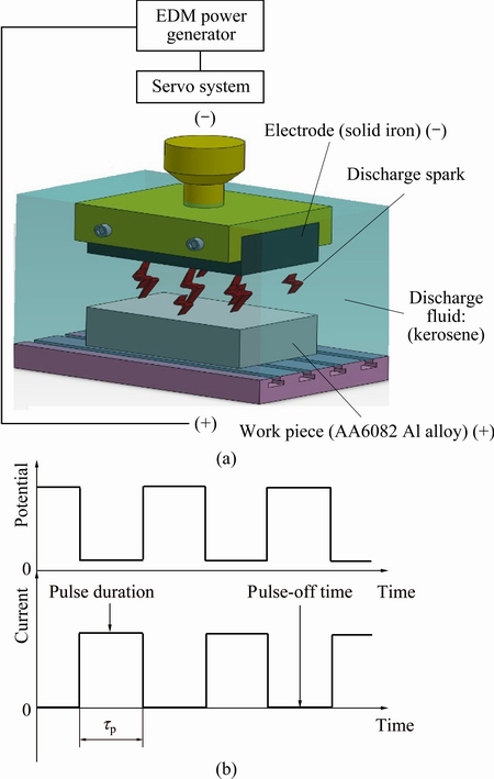
Fig. 1 Schematic of apparatus used to carry out electrical discharge alloying process, with electrical discharge occurring between solid iron electrode (-) and 6082 work piece (+) (a) and electrical discharge square waveform used (b) (Electrical discharge square wave form was used)
Table 1 Conditions of electrical discharge alloying process
Table 2 Pulse durations (0.5-3.0 ms) vs their corresponding single pulse energy in EDA process (taking discharge current 30 A as an example)
2.2 Analyses of microstructure and tribological properties
A scanning electron microscope (SEM: JEOL JSM-6700F) was used to examine the microstructure of the alloyed layer, and an electron probe microanalyzer (EPMA: JEOL 8900R) was utilized to analyze the distributions of chemical elements within the alloyed layer. The thickness of the alloyed layer was measured by SEM cross-section view.
A field emission gun (FEG) transmission electron microscope (TEM: Tecnai G2), equipped with a high-angle annular dark field (HAADF) detector, was utilized to analyze the microstructure of the alloyed layer on the specimens. The intensity of the HAADF image is strongly related to the atomic number (z contrast) [37]. In the TEM analysis, an accelerating voltage of 120 kV was used. The TEM was equipped with an energy dispersive spectrometer (EDS) system that supported semi- quantitative elemental microanalysis of a selected area. TEM samples were prepared using the focus ion bean method (FIB: JEOL JIB-4601 F). TEM foils from the alloyed layers and from positions close to the heat-affected zone were taken. Before the FIB approach was implemented, a gold (Au) film was deposited on the area of interest of the surface of the sample to protect it from ion damage. The thickness of the TEM foil sample was around 80 nm.
Surface roughness, Ra (mm), of each sample was measured by Kosaka surfcorder SE3500 (Kosaka Lab. Ltd., Tokyo, Japan). The tribological properties of AA6082 and the EDA-layered 6082 alloys were tested on a standard pin-on-disc tribotester with a load of 8 N over a total sliding distance of 2100 m. The counterface material was silicon nitride (Si3N4) with a hardness of HV 1500, in the form of a ball with a diameter of 6.35 mm (0.25 inch). This tribotester was used for pure sliding with rotational motion at a constant speed of 50 r/min. The torque that was developed between the surfaces in sliding contact was detected using a torque measuring system, so the value of the friction coefficient throughout the test was determined. The mass loss was measured for each specimen by weighing the specimen before and after each wear test. At least three tests for each kind of specimen were performed, and then their wear rates (mg/m) were calculated.
2.3 Precipitation and high-temperature re-solid solution in sublayer beneath EDA coating
As described above, the two types of substrates used herein were as-received 6082-T651 and solid solution- treated 6082-T4 (Solu_6082), both with dimensions of 50 mm ЎБ 30 mm ЎБ 13 mm. The matrix of the as-received substrate specimen contained precipitates. When electric discharge occurred between the electrodes, the precipitates in the substrates immediately beneath the newly formed alloyed layer may have been over-aged or re-dissolved into solid solution. In the latter case, the heat input during electric discharge may have been high enough to have preserved the solid solution under the alloyed layer. This work considers phase stability in relation to precipitation and solid solution, with reference to the relationship between precipitation and the hardness of the material. Discharge currents of 15, 20 and 30 A were applied. Aging treatment was performed by placing the alloy specimens in a circulating silicone oil bath at a constant temperature of 170 ЎгC for 4 h. The macro- hardness of each sample was evaluated on the Rockwell F scale by indenting the alloyed layer normal to the surface of the sample using a steel ball indenter with a diameter of 0.159 cm (1/16 inch) and a test load of 600 N. A Vickers micro-hardness tester was used to measure the hardness of cross-sections of the polished specimens. The measurements were made using a load of 25 g for 15 s at 10 ҰМm intervals from the alloyed layer to the substrate.
2.4 Hysteresis curve and EMI test of EDA layer on aluminum alloy
No previous investigation has measured the magnetic properties of an alloyed layer that is formed using an electric discharge machine. Herein, the magnetic hysteresis of an alloyed layer was analyzed using a superconducting quantum interference device (SQUID). The hysteresis loop of the substrate (AA6082) was also measured for comparison. The effectiveness of EMI shielding was measured using a vector network analyzer (R&S ZVL) at frequencies from 9 kHz to 1 GHz, based on IEC standard 61967-6. Figure 2 schematically depicts the apparatus for measuring EMI. The samples were obtained under different electric discharge conditions, and all had dimensions of 50 mm ЎБ 30 mm ЎБ 2 mm. The alloyed layer on each sample had an area of 50 mm ЎБ 30 mm.
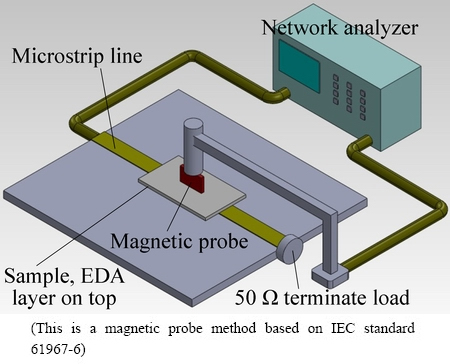
Fig. 2 Schematic of apparatus used to measure samplesЎҜ electromagnetic interference (EMI) shielding effectiveness
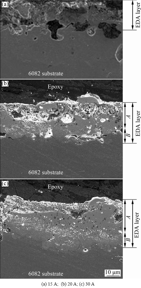
Fig. 3 SEM images of cross-section of alloying layers owing to various discharge currents used (all having the same pulse duration of 3.0 ms. The EDA layer was composed of alloy layer (denoted as A) and heat-affected zone (denoted as B))
3 Results and discussion
3.1 Cross-sectional and surface microstructural observations and analysis of EDA layer
Figure 3 shows the microstructures of the EDA layers under discharge currents of 15, 20 and 30 A with pulse duration of 3 ms. The EDA layer and the substrate are indicated in the figure. Figure 3(a) (discharge current of 15 A) shows a damaged alloyed layer on the 6082 substrate. When the discharge current was increased to 20 A (Fig. 3(b)), the thickness of the EDA layer increased; this layer contained both an alloyed layer (A) and a heat-affected zone (B). Figure 3(c) shows a relatively thick EDA layer on the sample that was processed using a discharge current of 30 A. The EDA layer comprised an alloyed layer (A) and a heat-affected zone (B). Figure 4 shows the effects of discharge current and pulse duration on the thickness of the alloyed layer. The thickness of the EDA layer increased with the increase of the pulse duration, regardless of the discharge current. The thickest alloyed layer, with a thickness of (29ЎА3) ҰМm, was obtained using a discharge current of 30 A and a pulse duration of 3.0 ms (Fig. 4). When the discharge current exceeded 30 A, surface cracks were formed on the alloyed layer (data not shown here). Therefore, a discharge current of 30 A was used to obtain the following experimental results. Figure 5(a) shows the mass loss of the Fe electrode as a function of pulse duration under the same discharge current of 30 A. For comparison, the mass loss of each workpiece under the same EDA process was also illustrated in Fig. 5(a). As shown in Fig. 5(a), the mass loss of Fe electrode is evidently larger than that of workpiece, fulfilling the basic concept of EDA process. Figure 5(b) plots the effect of pulse duration on the surface roughness of the alloyed layer that was processed using a discharge current of 30 A. The surface roughness of the specimens declined as the pulse duration increased; the roughness, which was specified as Ra value, declined from (7.5ЎА0.8) (at 30 A for 0.5 ms) to (5.6ЎА0.5) ҰМm (at 30 A for 3.0 ms) (Fig. 5(b)). STAMBEKOVA et al [24] utilized a pure Si electrode in an electrical discharge alloying process to modify 5083 aluminum alloy, and found that the surface roughness (Ra) increased from 3.1 to 3.8 ҰМm as the pulse duration increased from 0.1 to 1.0 ms at a discharge current of 30 A. KIYAK and  [38] found that, in the application of EDM to a steel sample, as the pulse duration was increased from 2 to 100 ҰМs, the surface roughness (Ra) increased from 2 to approximately 10 ҰМm. Thus, the findings of the present study, which reveal that the surface roughness declined as the pulse duration increased, differed from those obtained in previous studies. A current of 30 A and a pulse duration of 3 ms in the electric discharge alloying process between the solid Fe electrode and the 6082 aluminum alloy workpiece were found herein to yield not only a thick EDA layer but also a relatively smooth surface.

Fig. 4 EDA layer thickness of samples respectively processed by 15, 20 and 30 A, showing relationship between thickness and pulse duration
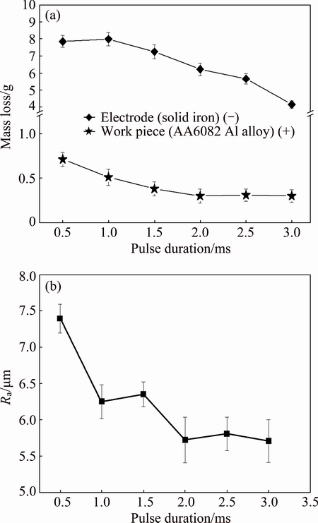
Fig. 5 Mass loss of iron electrode (-) and workpiece sample (+) as function of pulse duration after EDA process (a) and surface roughness (Ra) of EDA layer versus pulse durations 0.5 to 3.0 ms under discharge current of 30 A (b)
Figure 6 shows the distributions of Al (Fig. 6(a)), Fe (Fig. 6(b)) and C (Fig. 6(c)) elements in the EDA layer and the substrate, which were obtained by electron probe microanalysis (EPMA) of a cross-section of the sample at 30 A and 3.0 ms. At the top of the figure, Ў°AЎұ denotes the alloyed layer and Ў°BЎұ denotes the heat-affected zone. The Al intensity map that was obtained by EPMA revealed that Al exhibited a gradient from the substrate (high Al content, in red) to the heat-affected zone (reduced Al content, in green), and finally to the alloyed layer (even lower Al content, in blue). Importantly, the black spheres (indicated by arrows) in Fig. 6(a) contained almost no Al. The element Fe, as displayed in Fig. 6(b), was present at a relatively high content in the alloyed layer (red); the Fe content was lower in the heat-affected zone (green) and the lowest (blue) was close to the substrate (Fig. 6(b)). The black spheres in Fig. 6(b) are in the same positions as in Fig. 6(a)), proving that these local spherical regions contained almost no iron and no aluminum. The carbon map in Fig. 6(c) reveals that those spherical regions contained high content of carbon. The high-carbon spherical regions were observed in both the alloyed layer and the heat-affected zone. Those spherical regions were probably graphite particles because they contained nearly all carbon and almost no Fe and Al.
Figure 7(a) presents an SEM backscattered electron image (BEI) of the surface of the sample at 30 A and 3.0 ms. Some phase regions are observed in strong contrast, and some are seen in weak contrast (e.g., see the circled region in Fig. 7(a)). Figures 7(b)-(d) respectively present EPMA mappings of Fe, Al and C signals from the area that is displayed in Fig. 7(a). Signals that are associated with Fe are intense on the sample surface. Some local regions (in red) exhibited intense Fe signals. The areas that yielded intense Fe signals were those appearing bright in Fig. 7(a). Figure 7(c) presents Al signals of low intensity on the mapped surface. Again, most of the circled region yielded almost no Al signal (Fig. 7(c)). Carbon was mapped in Fig. 7(d).
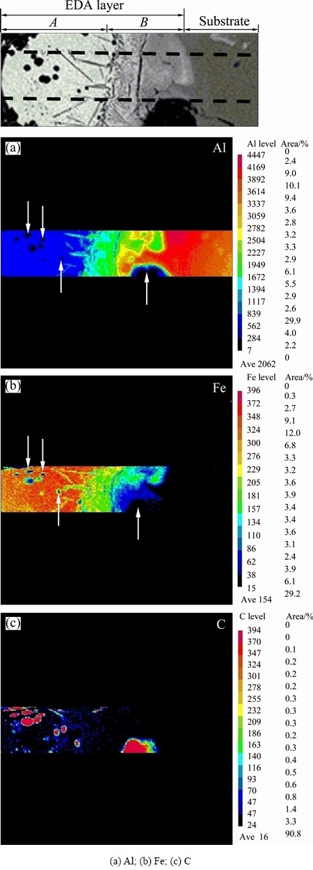
Fig. 6 EPMA mapping microanalysis of EDA layer for chemical elements (The EDA layer was composed of alloy layer (denoted as A) and heat-affected zone (denoted as B)
The dark regions (such as those in the circle in Fig. 7(a)) exhibited remarkably intense carbon signals (as shown in Fig. 7(d)). The pyrolysis of kerosene yielded the condensed carbon phase. As presented in Fig. 7(d), the condensed carbon phase was widely distributed on the EDA sample surface.

Fig. 7 Surface topography and elements distribution for EDA-processed 6082 Al alloy at 30 A with pulse duration of 3.0 ms
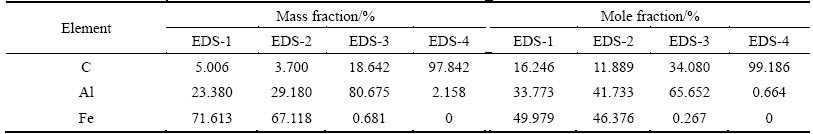
Figure 8 presents TEM images of the alloyed layer at 30 A and 3.0 ms. Figure 8(a) presents a dendritic solidified microstructure at low magnification. An HAADF image clearly reveals the differences between the Al and Fe contents of the dendritic core (dark) and those of the inter-dendritic phase (bright) (as shown in Fig. 8(b)). Figure 8(c) (a higher magnification image) clearly reveals the dendritic core (in dark) and inter-dendritic phases (in bright). Selected-area EDS analysis (Table 3) shows that the dendritic core contains ~16% C, ~16% Al and ~69% Fe (mole fraction), whereas the inter-dendritic phase contains ~16% C, ~3% Al and ~81% Fe (mole fraction). Figure 9(a) presents TEM image of the heat-affected zone, which reveal rod-like and round particles throughout the matrix. As shown in Fig. 9(b), a high-magnification image reveals that the matrix was polycrystalline, with a grain size of approximately 50 nm. EDS-1 and EDS-2 suggest that the matrix contained ~36% Al, ~48% Fe (mole fraction) (Table 4) and the remaining of carbon. EDS-3 presents the chemical composition of the white rod-like material (Fig. 9(b)), and suggests that the main chemical components are aluminum and carbon (with Fe at only ~0.27%, mole fraction). Based on the mole fractions of Al and C in EDS-3, the chemical formula of the rod-like particles is Al2C (which are denoted hereafter as Al2C-like particles). CHERTIHIN et al [39] prepared di-aluminum carbide (Al2C) by reacting pulsed-laser- evaporated Al with C and C2H2. They only examined the carbide by FTIR, and did not elucidate its microstructure or morphology. JARFORS et al [40] studied the thermodynamics and kinetics of carbides in the aluminum-rich corner of the Al-Ti-C phase diagram. They considered only the carbides Al4O4C and Al4C3 and conducted no TEM or SEM examination and presented no EDS analysis. Hence, this work firstly discovered Al2C-like particles in the EDA layer. Most importantly, Fig. 9(c) shows a high-magnification image of the microstructure of the spherical particles, which revealed that the structure was radial. The results of the EDS-4 analysis indicated that these spherical particles contained 99% C, suggesting that they were graphite. KUMAR et al [41] prepared a carbon film on a substrate at 800- 1000 ЎгC by the high-temperature pyrolysis of kerosene.
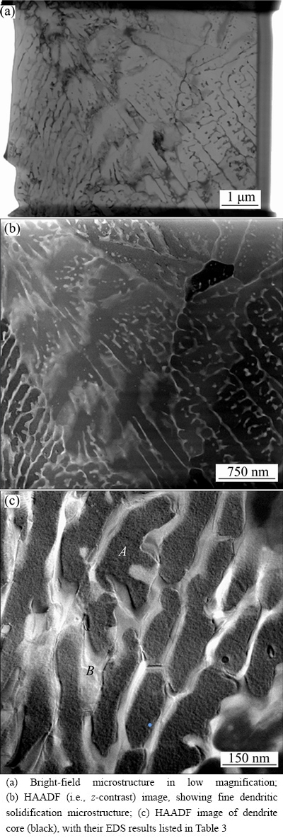
Fig. 8 TEM images and EDS analysis of alloy layer
Table 3 EDS analysis obtained from zones A and B in Fig. 8(c)
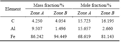
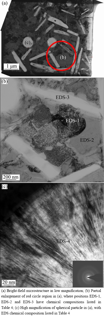
Fig. 9 TEM images and EDS analysis of TEM foil sample from heat-affected zone (see zone denoted in Figs. 3 and 6)
Herein, when electrical discharge occurred between the electrode and the workpiece, high temperature plasma (8000 and 12000 ЎгC) can be generated [15,42]. At the sparking of the discharge, the dielectric fluid (kerosene) underwent pyrolysis on account of the high temperature [22,43]. Therefore, a strong carburizing atmosphere was generated, causing carburization in the alloyed layer. Carbides were thus formed, and excess carbon became graphite (Figs. 6, 7 and 9), existing in the recast surface layer on workpiece.
Table 4 EDS analysis of TEM foil sample from heat-affected zone
3.2 Hard EDA layer on aluminum alloy and recovery of hardness in sublayer region
Figure 10(a) shows the effect of aging at 170 ЎгC on the microhardness from the alloyed layer to the substrate. The sample was as-received AA6082 aluminum alloy, which was treated by electric discharge alloying at 15 A. This sample was specified as as-received EDA-15 A before it was aged at 170 ЎгC for 4 h, after which the sample was denoted as as-received EDA-15 A/ 4 h_aging@170 ЎгC. As presented in Fig. 10(a), the EDA-modified layer had a microhardness of HV ~1450. The hardness of the EDA layer was almost equal to that of as-received EDA-15 A/4 h_aging@170 ЎгC. The hardness of the sublayer in the as-received EDA-15 A sample was much lower, being HV ~110 (which was less than that of the substrate, HV ~130). Since the as-received substrate alloy was originally precipitation hardening (HV ~130), the heating energy that was generated during a electric discharge at 15 A may have caused over-aging of the sublayer. Our earlier investigation [44] of the over-aging of Al-Mg-Si aluminum alloy found that over-aging slightly reduced the hardness of the material. Therefore, further treatment of the sample at 170 ЎгC (i.e., as-received EDA-15 A/ 4 h_aging@170 ЎгC in Fig. 10(a)) reduced the hardness of the sublayer region to HV ~100 because this sublayer was then aged twice. FARHANI et al [45] suggested that a hard surface layer may break out if the sublayer beneath it provides only weak support. For the purposes of this work, knowing how to recover the hardness of the sublayer following the EDA process on the 6082 alloy is important. A high electrical discharge current (30 A) was used in the EDA process. The heating energy that was generated during a electrical discharge at 30 A may have been sufficiently high to turn the sublayer into a solid solution. As presented in Fig. 10(b), the hardness of the sublayer in the as-received EDA-30 A was considerably reduced to HV 50, probably because the original precipitates in the sublayer dissolved into solid solution during the EDA process. The thickness of the sublayer was ~50 mm. Importantly, the hardness of the sublayer was recovered to ~HV 240 after aging treatment at 170 ЎгC for 4 h (i.e., the sample of as-received EDA-30 A/4 h_aging@170ЎгC in Fig. 10(b)), owing to precipitation hardening from solid solution. Figure 11 reveals the importance of the sublayer hardness in determining the HRF hardness of the EDA sample. The dotted line in Fig. 11 represents the HRF hardness of the 6082 aluminum alloy substrate that was firstly solution-treated and then aged at 170 ЎгC for 4 h. This sample was denoted as solu_4 h_aging@170 ЎгC, and had a hardness of HRF ~86. The solu_as EDA-30 A samples in Fig. 11 are the 6082 samples that firstly were solution-treated and then underwent the EDA process with pulse durations of 0.5-3.0 ms at a discharge current of 30 A. A Rockwell hardness indenter was pressed normally into the surface of the sample. As presented in Fig. 11, the hardness of solu_as EDA-30 A was only HRF 40, independently of the pulse duration that was used in the EDA process. Importantly, aging treatment at 170 ЎгC for 4 h was performed to improve the EDA sampleЎҜs sublayer hardness, and thus could greatly increase the sampleЎҜs hardness to HRF ~92.
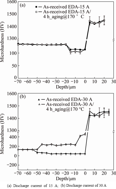
Fig. 10 Microhardness profiles from EDA layer to subsurface under pulse duration of 3.0 ms, showing effect of 170 ЎгC aging treatment on profiles
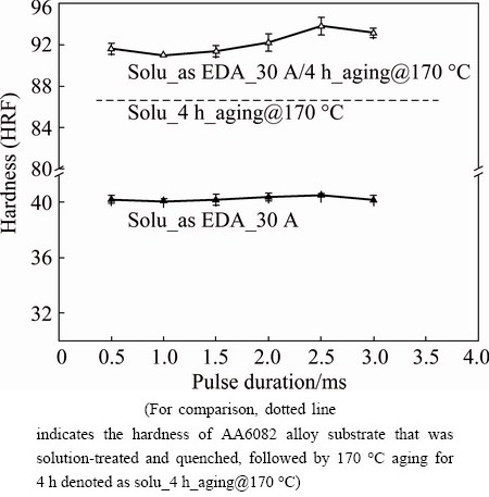
Fig. 11 Hardness data lines of solu_as EDA-30 A and solu_as EDA-30 A/4 h_aging@170 ЎгC samples showing importance of heat treatment on HRF hardness
3.3 Tribological properties of EDA-layered Al-Mg-Si aluminum alloy
Figure 12 shows the evolution of the friction coefficient during sliding tests over a distance of 2100 m with a normal load of 8 N. As presented in Fig. 12, the friction coefficient of the AA6082 aluminum substrate fluctuated as a function of sliding distance. The friction coefficients rapidly increased to 0.981 and 0.793 during the first 60 m of sliding, mainly owing to the highly plastic deformation that was caused by the sliding contact between the counterface material (Si3N4) and the Al alloy surface. Metallic aluminum adhered to the Si3N4 ball, increasing the friction coefficient. Strain hardening reduced the plastic deformation, reducing the friction coefficient during sliding through a distance from 250 to 2100 m. On the other hand, the EDA-layered sample had a much lower friction coefficient and wear rate than the Al substrate sample. The friction coefficient of the as-received EDA-30 A sample was initially ~0.054, and this very low value was maintained throughout the sliding test. The as-received EDA-30 A/4 h_aging@ 170 ЎгC sample also had a low friction coefficient of 0.112 after the first sliding distance of 60 m, descending to 0.055 at a sliding distance of 2100 m. The wear rate of the 6082 aluminum alloy substrate after the tests was (1.07ЎА0.09)ЎБ10-2 mg/m. The wear rate of the as-received EDA-30 A sample was only (2.78ЎА0.28)ЎБ10-4 mg/m and that of the as-received EDA-30 A/4 h_aging@170 ЎгC sample was as low as (1.79ЎА0.74)ЎБ10-4 mg/m, both values are two orders of magnitude less than that of the AA6082 substrate. MALAYOGLU et al [9] studied the tribological properties of plasma electrolytic oxidized (PEO) and hard-anodized (HA) coatings on 6082 Al alloy. They investigated the wear behaviors of these coatings under dry and oil-lubricated conditions by performing ball-on-plate tests using an Si3N4 ball with diameter of 12.7 mm under normal loads of 10, 20 and 100 N. The friction coefficient of the dry HA coating was ~0.8, and that of the dry PEO coating was also ~0.8 [9]. The oil-lubricated PEO and HA coatings on 6082 Al alloy had friction coefficients of only ~0.1 [9]. WANG et al [46] found a similar discrepancy between the friction coefficient of the non-lubricant anodic coating and that of the lubricated anodic coating: the anodic coating had a friction coefficient of ~0.6 and the oil-lubricated one had a coefficient of ~0.2. Based on the cited studies, lubricating hard oxide films on aluminum alloy reduces the friction coefficient to a relatively low value. In this work, the EDA process automatically generated both graphite spots on the as-EDA layer surface and graphite particles within the layer. The carbide in the layer was hard. Owing to the self-lubrication of the hard EDA layer, the friction coefficient of the EDA layer reached as low as ~0.07, following sliding wear through a distance of 2100 m. For comparison, the friction coefficient of the EDA layer obtained by LEE et al [22] and that of the EDA layer that was obtained by MORO et al [47] was one order of magnitude higher than those obtained herein. No graphite particles were generated in the modified layers in Refs. [22,47].
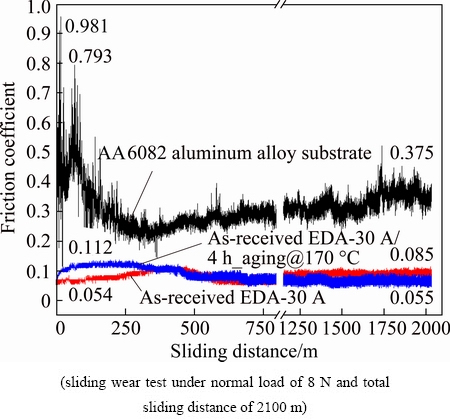
Fig. 12 Evolution of friction coefficient as function of sliding distance
3.4 Magnetic hysteresis of EDA layer and effectiveness of electromagnetic shielding by EDA-layered aluminum alloy plate
This investigation is to study the magnetism of a surface modification layer on aluminum alloy using the electric discharge process. Figure 13 shows the magnetic hysteresis loops of the EDA layers that were obtained with various electric pulse durations (0.5-3.0 ms). For comparison, Fig. 13 plots the hysteresis of the AA6082 aluminum alloy substrate. As shown in Fig. 13, AA6082 aluminum alloy (substrate) is non-magnetic. All of the hysteresis loops of the EDA layers were very thin, suggesting that the EDA layer was easily magnetized. Therefore, its coercivity was fairly low and a small reverse field sufficed to reduce its magnetization to zero. Importantly, the saturation value of the magnetism of an EDA layer depends on the electric pulse duration. The saturation values of 1.5-3.0 ms EDA layers considerably exceeded those of the 0.5 and 1.0 ms samples. This study shows that the electrical discharge process can not only improve the surface mechanical properties of aluminum alloy but also easily yield a softly magnetic layer on a non-magnetic substrate. Figure 14 shows the effect of frequency on the effectiveness of EMI shielding by the EDA-layered AA6082 plate samples. For comparison, Fig. 14 also shows the effectiveness of EMI shielding by the AA6082 sample without EDA layer. When the frequency increased from zero to 0.3 GHz (Fig. 14(a)), the effectiveness of EMI shielding by the 3.0 ms EDA-layered AA6082 sample was approximately 28 dB, which slightly exceeded that of the AA6082 substrate sample. Aluminum alloy is well known to be one of the most useful lightmass materials. With respect to EMI shielding, aluminum and aluminum alloys are commonly used to protect against 50 and 60 Hz electromagnetic fields that are generated by transformers and other devices [48]. The 3.0 ms EDA surface treatment process improves the effectiveness of EMI shielding by aluminum alloy against electromagnetic fields at relatively high frequencies of ~0.2 GHz. Figure 14(b) reveals that the electromagnetic shielding effectiveness of the EDA sample exceeds that of the AA6082 substrate sample at frequencies of 0.4-0.8 GHz. At a frequency of 0.5 GHz, the 2.0 and 2.5 ms EDA-layered 6082 exhibited shielding effectiveness of ~37 dB while the AA6082 substrate sample provided a shielding effectiveness of only ~28 dB. For frequencies between 0.55 and 0.6 GHz, the 1.5 ms-EDA layered AA6082 sample provided a shielding effectiveness of ~40 dB while AA6082 aluminum alloy exhibited a shielding effectiveness of only ~32 dB. In practice, industry typically requires an EMI effectiveness of 30-60 dB [49]. Electroless Ni-P, Ni-Co-P and Ni-P-La deposition coatings on aluminum substrates [49] and on plastic substrates [50] have been examined mostly with respect to their effectiveness in shielding against the electromagnetic waves. Coating the surface of an 6082 aluminum plate sample using by EDA process with a discharge current of 30 A and a high pulse duration increased its electromagnetic shielding effectiveness by 1-9 dB.
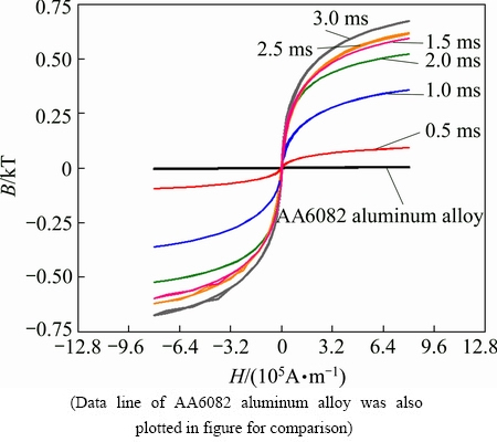
Fig. 13 Hysteresis curves of different EDA layers, each processed at discharge current of 30 A with different pulse durations

Fig. 14 EMI shielding effectiveness of 2 mm-thick AA6082 plates with and without EDA layer, tested in different frequency ranges
4 Conclusions
1) An electrical discharge alloying method, using a metallic solid pure iron as a negative electrode (the consuming electrode), was successfully developed to form a hard self-lubricated layer on AA6082 Al-Mg-Si aluminum alloy substrate. A discharge pulse duration of 3.0 ms and a discharge current of 20-30 A at ambient temperature in kerosene were found to optimize the EDA surface modification process.
2) The hard self-lubricated layer was a multi-phase material containing carbides and graphite. TEM observation verified that the carbide in the EDA layer had a fine dendritic microstructure. The chemical composition of the dendrite core was ~68.6% Fe, ~15.7% Al and ~15.7% C, while the interdendritic constituents had a chemical composition of ~81.1% Fe, ~2.7% Al and ~16.2% C. Al2C-like carbide particles (~0.27% Fe, ~65.7% Al and ~34.1% C) were found in the modified layer close to the substrate. Small graphite particles were distributed throughout the carbide layer. Moreover, irregular graphite spots on the carbide layer surface were observed.
3) The friction coefficient of the EDA layer surface remained approximately constant at a low value of ~0.07 throughout the sliding wear test with a sliding distance of 2100 m under a normal load of 8 N. The mean wear rate of the EDA-layered sample after the sliding wear test was as low as (1.79ЎА0.74)ЎБ10-4 mg/m. In contrast, owing to the heavy plastic deformation under the same loading on the AA6082 Al-Mg-Si substrate during the sliding wear test, the friction coefficient of the substrate metal reached ~0.9, and its wear rate was as high as (1.07ЎА0.09)ЎБ10-2 mg/m.
4) The bulk Rockwell hardness (HRF) of the EDA-modified sample was not only attributed to the hard surface layer on AA6082 aluminum alloy but partly assigned to a strong sublayer which exhibited sufficient strength to support the EDA surface layer. Importantly, a high discharge current must be used to prevent over-aging precipitation in the sublayer. In this work, discharge currents of 20 and 30 A yielded sublayers in solid solution, thus hardness was recovered by a simple aging treatment at 170 ЎгC for 4 h.
5) SQUID data reveal that modifying the surface of aluminum alloy by the EDA process increased its magnetization. Despite the fact that aluminum alloy is an effective EMI shielding material, the EDA coating layer on the aluminum alloy improved the EMI shielding effectiveness of the alloy by 1-9 dB.
References
[1] Belingardi G, OBRADOVIC J. Recent development in car body lightweight designЎӘA contribution toward greener environment [J]. Mobility and Vehicle Mechanics, 2012, 38: 9-23.
[2] DADBAKHSH S, KARIMI TAHERI A, SMITH C W. Strengthening study on 6082 Al alloy after combination of aging treatment and ECAP process [J]. Mater Sci Eng A, 2010, 527: 4758-4766.
[3] EDWARDS G A, STILLER K, DUNLOP G L, COUPER M J. The precipitation sequence in Al-Mg-Si alloys [J]. Acta Mater, 1998, 46: 3893-3904.
[4] MURAYAMA M, HONO K. Pre-precipitate clusters and precipitation processes in Al-Mg-Si alloys [J]. Acta Mater, 1999, 47: 1537-1548.
[5] MARIOARA C D, ANDERSEN S J, JANSEN J, ZANDBERGEN H W. The influence of temperature and storage time at RT on nucleation of the ҰВ " phase in a 6082 Al-Mg-Si alloy [J]. Acta Mater, 2003, 51: 789-796.
[6] BARAGETTI S, LA VECCHIA G M, TERRANOVA A. Variables affecting the fatigue resistance of PVD-coated components [J]. Int J Fatigue, 2005, 27: 1541-1550.
[7] VENCL A, BOBIC I, JOVANOVIC M T, BABIC M, MITROVIC S. Microstructural and tribological properties of A356 Al-Si alloy reinforced with Al2O3 particles [J]. Tribol Lett, 2008, 32: 159-170.
[8] BARIK R C, WHARTON J A, WOOD R J K, STOKES K R, JONES R L. Corrosion, erosion and erosionЁCcorrosion performance of plasma electrolytic oxidation (PEO) deposited Al2O3 coatings [J]. Surf Coat Technol, 2005,199: 158-167.
[9] MALAYOGLU U, TEKIN K C, MALAYOGLU U, SHRESTHA S. An investigation into the mechanical and tribological properties of plasma electrolytic oxidation and hard-anodized coatings on 6082 aluminum alloy [J]. Mater Sci Eng A, 2011, 528: 7451-7460.
[10] YUREKTURK Y, MUHAFFEL F, BAYDOGAN M. Characterization of micro arc oxidized 6082 aluminum alloy in an electrolyte containing carbon nanotubes [J]. Surf Coat Technol, 2015, 269: 83-90.
[11] KUHN A T. Plasma anodized aluminumЎӘA 2000/2000 ceramic coating [J]. Met Finishing, 2002, 100: 44-50.
[12] HO K H, NEWMAN S T. State of the art electrical discharge machining (EDM) [J]. Int J Mach Tools Manuf, 2003, 43: 1287-1300.
[13] KUMAR S, SINGH R, SINGH T P, SETHI B L. Surface modification by electrical discharge machining: A review [J]. J Mater Process Technol, 2009, 209: 3675-3687.
[14] TSAI Kuo-Ming, WANG Pei-Jen. Predictions on surface finish in electrical discharge machining based upon neural network models [J]. Int J Mach Tools Manuf, 2001, 41: 1385-1403.
[15] BOOTHROYD G, WINSTON A K. Non-conventional machining processes, in: Fundamentals of machining and machine tools [M]. New York: Marcel Dekker Inc, 1989: 491.
[16] SINGH A, GHOSH A. A thermo-electric model of material removal during electric discharge machining [J]. Int J Mach Tools Manuf, 1999, 39: 669-682.
[17] GANGADHAR A, SUNMUGAM M S, PHILIP P K. Pulse train studies in EDM with controlled pulse relaxation [J]. Int J Mach Tools Manuf, 1992, 32: 651-657.
[18] MOHRI N, SAITO N, TSUNEKAWA Y, KINOSHITA N. Metal surface modification by electrical discharge machining with composite electrode [J]. Anal CIRP, 1993, 42: 219-222.
[19] TSUNEKAWA Y, OKUMIYA M, MOHRI N, TAKAHASHI I. Surface modification of aluminum by electrical discharge alloying [J]. Mater Sci Eng A, 1994, 174: 193-198.
[20] TSUNEKAWA Y, OKUMIYA M, MOHRI N, KURBE E. Surface modification of aluminum matrix composites by electrical discharge alloying [J]. Mater Sci Forum, 1996, 217-222: 1661-1666.
[21] YAN Biing-Hwa, LIN Yan-Cherng, HUANG Fuang-Yuan, WANG Chen-Hung. Surface modification of SKD 61 during EDM with metal powder in the dielectric [J]. Mater Trans JIM, 2001, 42: 2597-2604.
[22] LEE H G, SIMAO J, ASPINWALL D K, DEWES R C, VOICE W. Electrical discharge surface alloying [J]. J Mater Process Technol, 2004, 149: 334-340.
[23] STAMBEKOVA K, LIN H M, UAN J Y. Surface modification of 5083 Al alloy by electrical discharge alloying processing with a 75 mass% Si-Fe alloy electrode [J]. Appl Surf Sci, 2012, 258: 4483-4488.
[24] STAMBEKOVA K, LIN H M, UAN J Y. Microstructural and corrosion characteristics of alloying modified layer on 5083 Al alloy by electrical discharge alloying process with pure silicon electrode [J]. Mater Trans JIM, 2012, 53: 1436-1442.
[25] SIDHU H S, BANWAIT S S. Analysis and multi-objective optimisation of surface modification phenomenon by EDM process with copper-tungsten semi-sintered P/M composite electrodes [J]. American Journal Mechanical Engineering, 2014, 2: 130-142.
[26] PATOWARI P K, SAHA P, MISHRA P K. An experimental investigation of surface modification of C-40 steel using W-Cu powder metallurgy sintered compact tools in EDM [J]. Int J Adv Manuf Technol, 2015, 80: 343-360.
[27]  Mathematical modelling of the electrical discharge mechanical alloying process [J]. Procedia CIRP, 2013, 6: 423-427.
[28] DAS A, MISRA J P. Experimental investigation on surface modification of aluminum by electric discharge coating process using TiC/Cu green compact tool-electrode [J]. Mater Sci Technol, 2012, 16(4): 601-623.
[29] AHMED A. Deposition and analysis of composite coating on aluminum using Ti-B4C powder metallurgy tools in EDM [J]. Mater Manuf Processes, 2016, 31(4): 467-474.
[30] MOHRI N, SAITO N, TSUNEKAWA Y, MOMIYAMA H. Metal surface modification by electrical discharge machining with composite electrode [J]. J Jpn Soc Prec Eng, 1993, 59: 625-630.
[31] CHEN S L, YAN B H, HUANG F Y. Influence of kerosene and distilled water as dielectrics on the electric discharge machining characteristics of Ti-6A1-4V [J]. J Mater Process Technol, 1999, 87: 107-111.
[32] CHEN Yuan-Feng, CHOW Han-Ming, LIN Yan-Cherng, LIN Ching-Tien. Surface modification using semi-sintered electrodes on electrical discharge machining [J]. Int J Adv Manuf Technol, 2008, 36: 490-500.
[33] COX J H, PIDGEON L M. The X-ray diffraction patterns of aluminum carbide Al4C3 and aluminum oxycarbide Al4O4C [J]. Canad J Chem, 1963, 41: 1414-1416.
[34] ASM Handbook Editing Group. Alloy phase diagram [M]. New York: American Society of Metals International, 1992.
[35] SCHICK H L. Thermodynamics of certain refractory compounds [M]. New York: Academic Press, 1966.
[36] SIMAO J, ASPINWALL D K, EL-MENSHAWY F, MEADOWS K. Surface alloying using PM composite electrode materials when electrical discharge texturing hardened AISI D2 [J]. J Mater Process Technol, 2002, 127: 211-216.
[37] PENNYCOOK S J, JESSON D E. High-resolution incoherent imaging of crystals [J]. Phys Rev Lett, 1990, 64: 938-941.
[38] KIYAK M, CAKIR O. Examination of machining parameters on surface roughness in EDM of tool steel [J]. J Mater Process Technol, 2007, 191: 141-144.
[39] CHERTIHIN G V, ANDREWS L, TAYLOR P R. Reactions of pulsed-laser-evaporated Al with C and C2H2: Infrared spectra and CASSCF calculations for AlC, Al2C, Al2C2, and AlC2H [J]. J Am Chem Soc, 1994, 116: 3513-3518.
[40] JARFORS J, FREDRIKSSON H, FROYEN L. On the thermodynamics and kinetics of carbides in the aluminium-rich corner of the Al-Ti-C phase diagram [J]. Mater Sci Eng A, 1991, 135: 119-123.
[41] KUMAR M, SHARON M, ANDO Y, ZHAO X. Electron field emission from carbon films grown from pyrolysis of kerosene [J]. Diamond and Related Materials, 2001, 10: 883-888.
[42] SHOBERT E I. What happens in EDM [M]. Dearbern, Michigan: Society of Manufacturing Engineers, 1983.
[43] ARUNKUMAR L, RAGHUNATH B K. Electro discharge machining characteristics of Mg/SiCp metal matrix composites by powder metallurgy (P/M) techniques [J]. Int J Eng Technol, 2013, 5: 4332-4338.
[44] CHEN Yue-Ting, WANG Dung-An, UAN Jun-Yen, HSIEH Tsung-Hsien, TSAI Te-Chang. Tensile strength and deformation microstructure of Al-Mg-Si alloy sheet by through-width vibration rolling process [J]. Mater Sci Eng A, 2012, 551: 296-300.
[45] FARHANI M, AMADEH A, KASHANI H, SAEED-AKBARI A. The study of wear resistance of a hot forging die, hard faced by a cobalt-base superalloy [J]. Mater Forum, 2006, 30: 212-218.
[46] WANG Hui, WANG Hao-Wei. Fabrication of self-lubricating coating on aluminum and its frictional behaviour [J]. Appl Surf Sci, 2007, 253: 4386-4389.
[47] MORO T, MOHRI N, OTSUBO H, GOTO A, SAITO N. Study on the surface modification system with electrical discharge machine in the practical usage [J]. J Mater Process Technol, 2004, 149: 65-70.
[48] TONG X C. Advanced materials and design for electromagnetic interference shielding [M]. New York: CRC Press, 2009.
[49] GAO Y, HUANG L, ZHENG Z J, LI H, ZHU M. The influence of cobalt on the corrosion resistance and electromagnetic shielding of electroless Ni-Co-P deposits on Al substrate [J]. Appl Surf Sci, 2007, 253: 9470-9475.
[50] XUAN Tian-peng, YANG Guang-zhou, YANG Li-lin, JU Zheng-ting. Study on electromagnetic shielding effectiveness of Ni-P-La alloy coatings [J]. Journal of Rare Earths, 2006, 24: 389-392.
Wang-Chih Chen1, Hung-Mao Lin2, Jun-Yen Uan1
1. Department of Materials Science and Engineering, National Chung Hsing University, 145 Xingda Rd., South Dist., Taichung City 40227, China;
2. Department of Mechanical Engineering, Far East University, Zhonghua Rd., Xinshi Dist., Tainan City 74448, China
ХӘ ТӘЈәІЙУГ·ЕөзәПҪр»Ҝ№ӨТХ¶ФAA6082 Al-Mg-SiКұР§УІ»ҜВБәПҪрҪшРРұнГжёДРФЎЈФЪ·ЕөзәПҪр»Ҝ№эіМЦРЈ¬ЧчОӘ№ӨЧчТәөДГәУНИИҪвіЙМјЈ¬ҙУ¶шРОіЙёҪЧЕУЪәПҪрұнГжөДЧФИу»¬Мј»ҜОпІгЎЈTEMҪб№ыұнГчЈ¬әПҪрұнГжРОіЙөДЧФИу»¬Мј»ҜОпІгОӘУЙМј»ҜОпәНКҜД«ЧйіЙөД¶аПаІДБПЎЈТтҙЛЈ¬ҫӯ·ЕөзәПҪр»ҜёДРФВБәПҪрөДДҰЛрВКј«РЎЈ¬ФјОӘ2ЎБ10-4 mg/mЈ¬¶шВБәПҪр»щМеөДДҘЛрВКФјОӘ1.1ЎБ10-2 mg/mЎЈПФИ»Ј¬ФЪВБәПҪрұнГжҫӯ·ЕөзәПҪр»ҜРОіЙөДМј»ҜОпОӘТ»ЦЦДЬёДЙЖәПҪрҝ№өзҙЕёЙИЕРФДЬөДИнҙЕМеЎЈ
№ШјьҙКЈәAl-Mg-SiВБәПҪрЈ»ұнГжёДРФЈ»·ЕөзәПҪр»ҜЈ»ЧФИ󻬣»ИИҪвМјЈ»ҝ№өзҙЕёЙИЕРФДЬ
(Edited by Wei-ping CHEN)
Corresponding author: Jun-Yen UAN; Tel: +886-4-22854913; Fax: +886-4-22857017; E-mail: jyuan@dragon.nchu.edu.tw
DOI: 10.1016/S1003-6326(16)64453-9

