Trans. Nonferrous Met. Soc. China 25(2015) 3258-3264
Characterization of SiC nanowires prepared on C/C composite without catalyst by CVD
Yi-cheng GE, Yun-qi LIU, Shuai WU, Huang WU, Pei-ling MAO, Mao-zhong YI
State Key Laboratory of Powder Metallurgy, Central South University, Changsha 410083, China
Received 17 November 2014; accepted 10 June 2015
Abstract: SiC nanowires were prepared on C/C composite surface without catalyst by chemical vapor deposition (CVD) using CH3SiCl3 as precursor. SEM images of the CVD-product reveal that some long nanowires have grown to tens of micrometers with some gathered as a ball. Some short nanowires agglomerate like chestnut shell with many thorns accompanied by some deposited nano-particles. XRD, Raman-spectrum and FTIR patterns indicate that the product is a typical ��-SiC. TEM images show that the nanowires have a wide diameter range from 10 to 100 nm, and some thin nanowires are bonded to the thick one by amorphous CVD-SiC. A SiC branch generates from an amorphous section of a thick one with an angle of 70�� between them, which is consistent with the [111] axis stacking angle of the crystal. SAED and fast Fourier transform (FFT) patterns reveal that the nanowires can grow along with different axes, and the bamboo-nodes section is full of stacking faults and twin crystal. The twisted SiC lattice planes reveal that the screw dislocation growth is the main mechanism for the CVD-SiC nanowires.
Key words: SiC nanowires; C/C composite; chemical vapor deposition; growth mechanism; characterization
1 Introduction
Carbon fiber reinforced carbon matrix composite (C/C composite) has been widely used as thermal structural material, for example, brake material, seal ring, rocket nozzle and throat insert, which is benefited from low density, low coefficient of thermal (COF), high special strength and thermal conductivity [1]. But one obvious defect, easily being oxidized in air above 450 ��C, has limited the application of C/C composite. Therefore, oxidation-resistance is a key technology for C/C composite to ensure the properties in harsh surrounding [2].
After decades of research, SiC has become a kind of good material to prepare oxidation- and ablation-resistant coating for C/C composite [3,4]. But thermal residual stress, caused by different COFs between C/C composite and SiC, would induce micro-crack and be a fatal defect for the coating to deteriorate the property when facing severe temperature changes [5].
SiC nanowires, with high elastic modulus and decent chemical stability, have been widely used to reinforce ceramic-matrix composite [6,7]. LI et al [8] prepared the nanowires to reinforce SiC coating for C/C composite using Ni or Co as catalyst and proved good effect. Therefore, it is worth preparing SiC nanowires at first, which could improve the bonding between C/C composite and the coating [9].
SiC nanowires can be gotten by chemical vapor deposition (CVD), hydrothermal reaction, in-situ reaction, precursor pyrolysis and so on. For example, QING et al [10] prepared SiC nanowires at low temperature using silica sol, glucose, urea, PAM and nitric acid as raw materials, but the oxygenated chemicals would react with carbon material and influence the property of C/C composite. EICK and YOUNGBLOOD [11] produced the SiC nanowires from the spinning of poly (carbomethylsilane) with pyrolysis to ceramic, LI et al [12] also got it by using the off-gas from polycarbosilane-derived SiC. It is an interesting and good challenge for the coating-preparation on C/C composite. LIU et al [13] prepared the nanowires by deposited silicon on carbon nanotube and then annealed it at 1200 ��C. KIM et al [14] synthesized the nanowires by a solid-vapor reaction between carbon nanowires and SiO vapor using Ni-Fe, Fe-Al and Ni-Fe-Al as catalysts. XU et al [15] and LIU et al [16] also got the nanowires by using CH3SiCl3 as raw materials and Ni as catalyst. Those technologies have produced the nanowires with good properties, but the catalyst is difficult to be removed thoroughly and the coating might be impure. Thus, it is necessary to prepare the nanowires on C/C composite surface without such residual metal- impurity.
Therefore, in this work, we prepared SiC nanowires on C/C composite surface without catalyst, and analyzed their nano-structure and CVD mechanism.
2 Experimental
C/C composite with the density of 1.83 g/cm3 was provided by Hunan Boyun New Material Company Limited, China. It was machined to dimensions of 30 mm �� 30 mm �� 5 mm firstly, followed by being polished with 3000# SiC abrasive paper, cleaned in alcohol using ultrasonic cleaner and then dried prior to the test.
The preparation of SiC nanowires was conducted in a home-made isotherm and isopiestic CVD furnace. CH3SiCl3 was used as a precursor with H2 as carrier- and dilution-gas. CVD temperature was selected in the range of 1000-1100 ��C under pressures of 0.5-1.0 kPa in the deposited area. The deposited time was chosen as 1-3 h.
The morphology and structure of the CVD-product were detected using an FEI-Nova Nano 230 SEM, a JEM2100F TEM and a D/max2550 XRD, respectively. Infrared spectrum of the product was detected using an AVATAR-360-FTIR Fourier transform infrared spectrometer with a resolution of 2 cm-1 and a scanning range of 500-4000 nm-1. Raman spectrum was detected using an ALMEGA confocal micro-Raman spectrometer with wave length of 32.81 nm.
3 Results and discussion
Figure 1 presents FESEM images of the product on C/C composite surface. As shown in Fig. 1(a), some SiC nanowires gather into a ball, some straight or curved nanowires are distributed on the surface randomly. Similar to this study, many researches using catalyst also produced such randomly-deposited SiC nanowires [12-15]. This indicates that similar nanowires can be obtained with or without catalyst. As shown in Fig. 1(b), the short aggregated nanowires, prepared using a modified CVD technique, look like some tightly accumulated Chinese chestnut shell with many thorns. As shown in Fig. 1(c), the short nanowires form an irregular multi-dimensional network. Furthermore, many nano-particles are found on the surface of nanowires, which indicates that the nanowires are favorable deposited sites for the following CVD matter. At the same time, we found many tiny pieces bonded with several crossed nanowires. This demonstrated that the flowing CVD-matter was blocked in the crossed nanowires region, which had to be deposited directly on the nanowires surface and grew, and then connected to form a large one [15]. However, it should be pointed out that the grown piece might block the following CVD-gas from infiltrating into the beneath layer, which would result in some closed-holes in the coating. As shown in Fig. 1(d), the randomly-deposited nanowires were bonded with C/C composite surface tightly. It might be a good 3D reinforcement phase for the following CVD coating [8]. In the meantime, many nano-hemispheric particles with different sizes are found to be deposited on C/C composite surface. It also revealed that some SiC particles nucleated and deposited directly on C/C composite surface, which could be the cores for the following nanowires or coating [13,15]. Thereafter, it is good supplement for the nanowires to reinforce the bonding between the coating and C/C composite.
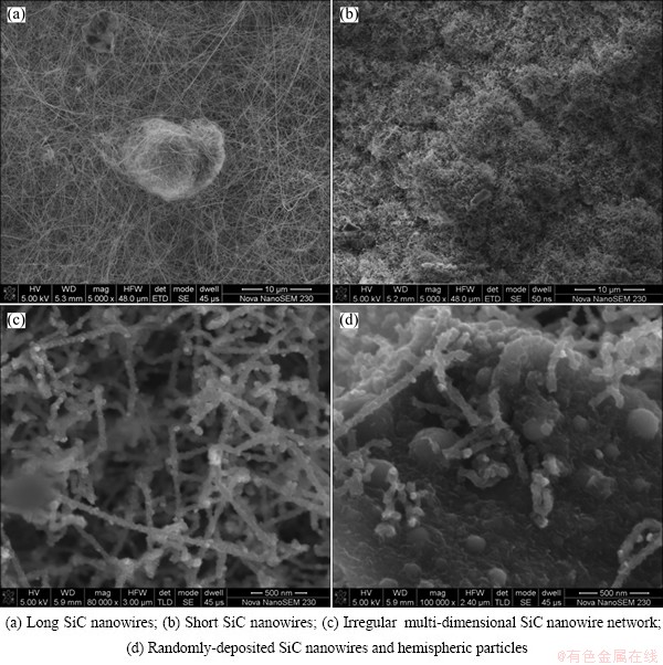
Fig. 1 FESEM images of SiC nanowires on C/C composite surface
Figure 2 shows XRD pattern of the product. It reveals that the nanowire is a typical ��-SiC with the diffraction peaks (2��) located at 35.6��, 59.9�� and 71.5��, which correspond to the (111), (220) and (311) crystal faces, respectively [6,7].

Fig. 2 XRD pattern of SiC nanowires
��-SiC has two peaks in Raman spectrum. One is a transverse optical (TO) mode at 796 cm-1, the other is longitudinal optical (LO) one at 972 cm-1 [6]. As shown in Fig. 3, two peaks present at 795 cm-1 and 972 cm-1, which are corresponding accurately to the TO and LO of ��-SiC, respectively.
Figure 4 shows a FTIR spectrum of SiC nanowires. It agrees with the results in Refs. [7,8]. A strong absorption peak at 804 cm-1 and a wide acromion close to 874 cm-1, correspond to the TO and LO of Si��C, respectively. BOROWIAK-PALEN et al [7] found that the peak at 804 cm-1 is shifted to low wave of 6 cm-1, which can be attributed to the small size effect of nano-material. Several weak peaks correspond to that of H2O and CO2 which are introduced during the testing.

Fig. 3 Raman spectrum of SiC nanowires

Fig. 4 FTIR spectrum of SiC nanowires
Figure 5 shows TEM and SAED images of the nanowires taken from C/C composite surface. As shown in Fig. 5(a), one straight large nanowire with the diameter of 100 nm can be found. A twisted one with similar diameter, which seems to generate from the straight one and connects with the straight one again can also be found. In addition, some small nanowires with the diameter of 10 nm, are bonded with a large one by extra-CVD-SiC. SAED pattern in Fig. 5(b), reveals that the wires are a face-centered cubic SiC. One pattern system shows that the nanowires have typical structure corresponding to [011] axis. The other pattern, corresponding to [111] axis, indicates that the nanowires can grow along with different directions. HRTEM image of the amorphous area near the branch, shown in Fig. 5(c), indicates that the normal deposition- process is disturbed due to the fluctuation or supersaturation of local CVD gas [17]. But the angle of 70��, between the trunk and the branch, is consistent with 70.53�� of any two adjacent (111) faces in cubic SiC crystal [18,19]. As shown in Fig. 5(d), two nanowires with bamboo-shape trunk are attached by some nano-particles. The interlamellar spacing of 0.25 nm in Fig. 5(e) reveals a typical (111) crystal plane of 3C-SiC in the trunk. As shown in Fig. 5(f), one FFT image (small inserted figure (f1)) gotten from Area A in the bamboo node, indicates a typical stacking faults or twin crystal due to the prolonged scattered spots [18]. The small figure (f2) from Area B, indicates a perfect 3C-SiC structure. But the SAED pattern for all areas, shown in small figure (f3), reveals that the nanowires grow along  axis. The rough edge is partly caused by the mixed arrangement of amorphous and regular SiC layer. It might be induced by the dangling bond, from silicon or carbon atoms, which resulted in an unbalance stress state for the surface atoms [19] and then forced some atoms or cells to deviate from the perfect lattice position. As shown in Fig. 5(g), a nano-particle with perfect 3C-SiC structure, is bonded with the trunk tightly by extra- amorphous CVD-SiC in the junction (marked with black arrow). The angle of 70��, measured from the lattice plane between the bonding SiC and the trunk, is also accorded with the growth rule of the (111) face. The amplified image, as shown in Fig. 5(h), reveals that the ball has grown along
  face.
face.
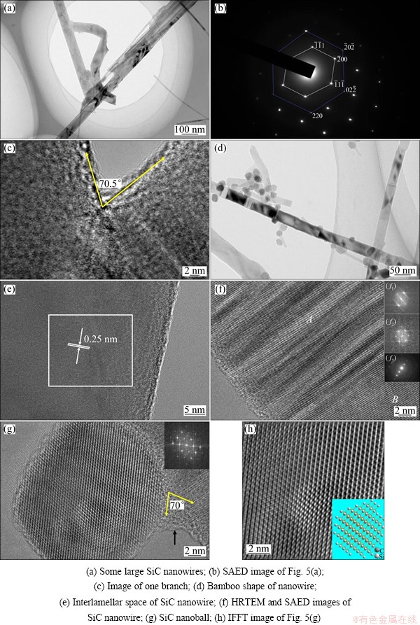
Fig. 5 TEM images and SAED pattern of SiC nanowires and nanoball
Figure 6 presents a magnified, IFFT and simulated images taken from the white block in Fig. 5(e). As shown in Figs. 6(a) and (b), a lot of stacking faults, dislocations and disordered area scatter randomly. This suggests that the residual stress induced by highly curved surface, irregularly arranged atom or atomic clusters near the surface and high free surface energy, would be released by such defects in the nanowires [20-22]. Therefore, it introduces tiny amorphous phase into the nanowires during the CVD process.
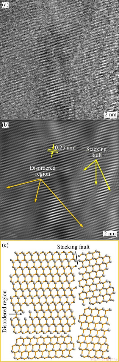
Fig. 6 Magnified (a), IFFT (b) and sketched (c) images of SiC nanowire taken from Fig. 5(e)
JIN et al [19] and KOH et al [23] found that screw dislocation growth was the main mechanism for SiC nanowires produced in vapor deposited process. HE et al [24] considered that anisotropic growth was the main reason and suggested that the nanowires were anisotropic materials and grew preferentially in a certain direction.
During the CVD process, MTS is decomposed into carbon, silicon, hydrogen atom or other different compounds as the following chemical equation [15]:
CH3SiCl3(g)��C��Hm(g) +Si��Cln(g) +HCl(g)��C��Hx(ad)+C(ad)+Si��Cln(ad)+H(g)��
C(ad)+ Si(ad)+xH(g)+nCl(g)��HCl(g)+SiC(s) (1)
where m, n, x=0, 1, 2, 3; ad represents adsorbed atoms; g represents gas; s represents solid.
According to the heterogeneous nucleation mechanism, it is easier for the new-generated atoms, cells or clusters to deposit, arrange and grow regularly on solid surface than to nucleate and grow only by themselves. Therefore, as shown in Fig. 1 and Fig. 5(e), most of the nanowires and hemispheric particles can be found to be deposited on the surface of C/C composite or the advanced-formed nanowires.
For the SiC nanowires, the tightest arrangement of atoms is along (111) and screw dislocation growth is the main mechanism [15]. Therefore, it is easy for the deposits, for example, carbon and silicon atoms, SiC- cell and cluster to deposit and grow along this plane due to the lowest energy. At the same time, the deposits would diffuse and topo-gather at the top of growing nanowires due to the concentration difference in the boundary layer [18], which restrains the nanowires to grow thick or only omit a little CVD-matter to deposit on the side surface. Some curved SiC crystal planes near the edge grow with screw dislocation which is similar to that of graphene [25]. The growth process of nanowires is presented in Fig. 7.
4 Conclusions
1) SEM images show that many straight or curved nanowires with length of tens of micrometers are distributed on the surface randomly with some gathered as a ball. Some short nanowires, gotten by a modified CVD technique, are agglomerated like chestnut shell with some deposited nano-particles. XRD, Raman and FTIR results reveal that the CVD-product is a typical ��-SiC.
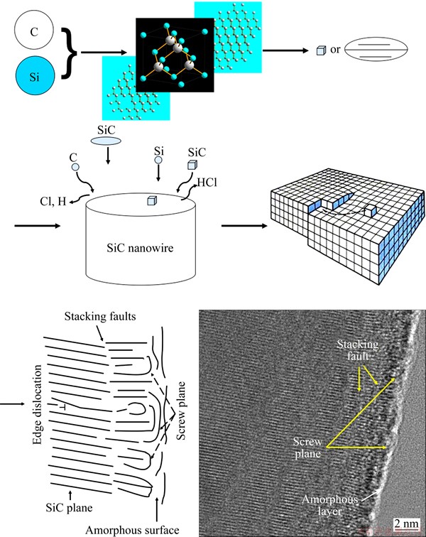
Fig. 7 Schematic diagrams of screw dislocation growth of SiC nanowires and their TEM image
2) TEM images show that the nanowires have a wide diameter from 10 to 100 nm. Some thin nanowires are bonded to thick one by amorphous SiC. SAED image indicates that the nanowires grow along different axes. In the bamboo node section, FFT image reveals that it is full of stacking faults or twin crystal, which can be proved by the prolonged scattered spots.
3) The intersection angle of 70��, measured from the amorphous section of branched SiC nanowires or from the bonded particle and nanowire trunk, is consistent with the (111) face growth mechanism of 3C-SiC crystal.
4) The screwed SiC lattice planes near the rough surface indicate the main mechanism of screw dislocation growth for the CVD nanowires.
References
[1] LEI Bao-ling, HE Lian-long, YI Mao-zhong, RAN Li-ping, XU Hui-juan, GE Yi-cheng, PENG Ke. New insights into the microstructure of the friction surface layer of C/C composites [J]. Carbon, 2011, 49(13): 4554-4562.
[2] GE Yi-cheng, YANG Ling-yun, WU Shuai, LI Chan, LUO Jian, YI Mao-zhong. Influence of heat-treatment on oxidation-resistance of phosphate-coating for C/C composite [J]. Transactions of Nonferrous Metals Society of China, 2014, 24(2): 455-461.
[3] LONG Y, JAVED A, SHAPIRO I, CHEN Z K, XIONG X, XIAO P. The effect of substrate position on the microstructure and mechanical properties of SiC coatings on carbon/carbon composites [J]. Surface and Coatings Technology, 2011, 206(2�C3): 568-574.
[4] XU Y J, ZHANG W H, CHAMORET D, DOMASZEWSKI M. Minimizing thermal residual stresses in C/SiC functionally graded material coating of C/C composites by using particle swarm optimization algorithm [J]. Computational Materials Science, 2012, 61(8): 99-105.
[5] QUAN G C, CONLON K T, WILKINSON D S. Investigation of whisker orientation in SiC whisker-reinforced alumina composites using neutron diffraction [J]. Journal of the European Ceramic Society, 2007, 27(1): 389-396.
[6] GOUADEC G, COLOMBAN P. Non-destructive mechanical characterization of SiC fibers by Raman spectroscopy [J]. Journal of the European Ceramic Society, 2001, 21(9): 1249-1259.
[7] BOROWIAK-PALEN E, RUEMMELI M H, GEMMING T, KNUPFER M, BIEDERMANN K, LEONHARDT A, PICHLER T, KALENCZUK R J.Bulk synthesis of carbon-filled silicon carbide nanotubes with a narrow diameter distribution [J]. Journal of Applied Physics, 2005, 97(5): 056102.
[8] LI Jun, TAN Zhou-jian, LIAO Ji-qiao, ZHANG Xiang, LI Bing-ju. Technology of in-situ growing SiCw on surface of C/C composites [J]. The Chinese Journal of Nonferrous Metals, 2012, 22(2): 427-433. (in Chinese)
[9] KAZAN M, TABBAL M, MASRI P. Infrared analysis of the effect of Ge at the interface between 3C-SiC and Si [J]. Diamond and Related Materials, 2012, 22(2): 23-28.
[10] QING Ming-li, CHU Ai-min, QU Xuan-hui, CAO Zhiq-qin, WU Hao-yang. A process for preparing silicon carbide nanowires: China, CN 103145129 A [P]. 2013-06-12. (in Chinese)
[11] EICK B M, YOUNGBLOOD J P. SiC nanowires by pyrolysis of electrospun preceramic polymers [J]. Journal of Materials Science, 2009, 44: 160-165.
[12] LI Gong-yi, LI Xiao-dong, WANG Hao, LIU Lin. Long SiC nanowires synthesized from off-gases of the polycarbosilane-derived SiC preparation [J]. Applied Physical A, 2010, 98: 293-298.
[13] LIU J W, ZHONG D Y, XIE F Q, SUN M, WANG.E G, LIU W X. Synthesis of SiC nanowires by annealing carbon nanotubes covered with Si [J]. Chemical Physics Letters, 2001, 348(5): 357-360.
[14] KIM J P, CHA H M, MYOUNG S W, LEE P H, LEE J H, JUNG Y G. Synthesis and microstructural characterization of silicon carbide nanowires from different carbon templates in a solid-vapor reaction [J]. Journal of Ceramic Processing Research, 2009, 10(3): 325-329.
[15] XU Xian-feng, XIAO Peng, XIONG Xiang, HUANG Bai-yun. Effects of Ni catalyzer on growth velocity and morphology of SiC nanowires [J]. Transactions of Nonferrous Metals Society of China, 2009, 19(5): 1146-1150.
[16] LIU Ye-qun, HE Lian-long, LU Xue-feng, XIAO Peng. Transmission electron microscopy study of the microstructure of carbon/carbon composites reinforced with in situ grown carbon nanowires [J]. Carbon, 2012, 50(7): 2424-2430.
[17] HAN X D, ZHANG Y F, ZHENG K, ZHANG X N, ZHANG Z, HAO Y J, GUO X Y, YUAN J, WANG Z L. Low-temperature in situ large strain plasticity of ceramic SiC nanowires and its atomic-scale mechanism [J]. Nano Letters, 2007, 7(2): 452-457.
[18] KUDRENKO E, RODDATIS A, ZHOKHOV A, ZVERKOVA I, KHODOS I, EMELCHENKO G. Morphology of SiC nanowires grown on the surface of carbon fibers [J]. RSC Advances, 2012(2): 4913-4919.
[19] JIN S, BIERMAN M J, MORIN S A. A new twist on nanowire formation: Screw-dislocation-driven growth of nanowires and nanotubes [J]. Journal of Physical Chemistry Letter, 2010, 1(9): 1472-1480.
[20] LIN M, LOH K P. Nanocantilevers made of bent silicon carbide nanowire-in-silicon oxide nanocones [J]. Applied Physics Letters, 2004, 85(22): 5388-5391.
[21] HAO X D, ZHANG Y F, LIU X Q, ZHANG Z, HAO Y J, GUO X Y. Lattice bending, disordering, and amorphization induced plastic deformation in a SiC nanowire [J]. Journal of Applied Physics, 2005, 98(12): 124307.
[22] ZHANG Yue-fei, HAN Xiao-dong, ZHENG Kun, ZHANG Ze, ZHANG Xiao-na, FU Jing-young, JI Yuan, HAO Ya-juan, GUO Xiaog-yun, WANG Zhong-lin. Direct observation of super-plasticity of beta-SiC nanowires at low temperature [J]. Advanced Functional Materials, 2007, 17(17): 3435-3440.
[23] KOH T L, O��HARA E C, GORDON M J. Microplasma-based synthesis of vertically aligned metal oxide nanostructures [J]. Nanotechnology, 2012, 23(42): 425603.
[24] HE J T, WANG Y W, FENG Y H, QI X Y, ZENG Z Y, LIU Q, TEO W S, GAN C L, ZHANG H, CHEN H Y. Forest of gold nanowires: A new type of nanocrystal growth [J]. ACS Nano, 2013, 7(3): 2733-2740.
[25] TERRONES H, LV R, TERRONES M, DRESSELHAUS M S. The role of defects and doping in 2D graphene sheets and 1D nanoribbons [J]. Reports on Progress in Physics, 2012, 75: 062501.
C/C���ϲ��ϱ�������CVD�Ʊ�SiC�����ߵĽṹ����
����ɣ����������� ˧���� �ʣ�ë���֣���ï��
���ϴ�ѧ ��ĩұ������ص�ʵ���ң���ɳ 410083
ժ Ҫ�������������£���CH3SiCl3Ϊǰ���壬���û�ѧ�����������(CVD)��C/C���ϲ��ϱ����Ʊ�SiC�����ߡ�SEM��ò������CVD�����д�����ʮ�׳��������ߣ������������ž۳���״��ͬʱҲ�������ƴ��̰�����ǵĶ������߾ۼ���������������������������XRD���������ͺ������������������˲���Ϊ���͵Ħ�-SiC��TEM��ò���������������ߵ�ֱ���ֲ���ΧΪ10~100 nm��һЩ��ϸ�������߿�ͨ������SiC��ϴֵ������߽����һ����һ���ϴ�SiC�����ߵ���������һ������ֱ������ķ�֧������֮��ļн�Ϊ70�㣬�����-SiC������[111]��Ѷ�н�һ�¡�SAED��FFT��������������ߵ��������߽϶࣬�������ߵ����״������ڴ����Ѷ������Ͼ�����Ե������SiC�����߾��������������λ������Ϊ����Ҫ���������ơ�
�ؼ��ʣ�SiC�����ߣ�C/C���ϲ��ϣ���ѧ����������������ƣ�����
(Edited by Wei-ping CHEN)
Foundation item: Project (201206375003) supported by the China Scholarship Council
Corresponding author: Yi-cheng GE; Tel: +86-731-88877700; E-mail: hncsgyc@163.com
DOI: 10.1016/S1003-6326(15)63962-0

