
Controlled synthesis of highly ordered CuO nanowire arrays by template-based sol-gel route
SU Yi-kun(苏轶坤)1, 2, 3, SHEN Cheng-min(申承民)2, YANG Hai-tao(杨海涛)2,
LI Hu-lin(力虎林)3, GAO Hong-jun(高鸿均)2
1. Shenzhen Key Laboratory of Special Functional Materials,College of Materials Science and Engineering, Shenzhen University, Shenzhen 518060, China;
2. Institute of Physics, Chinese Academy of Sciences, Beijing 100080, China;
3. School of Chemistry and Chemical Engineering, Lanzhou University, Lanzhou 730000, China
Received 1 February 2007; accepted 14 May 2007
Abstract: The highly ordered CuO nanowire arrays of composite-oxides were synthesized within a porous anodic aluminum oxide(AAO) template by a citrate-based sol-gel route. A vacuum system was applied to draw the gel into the template pores, which conquers the only driving force of this technique―capillary action, then the gel was thermally treated to prepare desired CuO nanowires. The results of scanning electron microscopy(SEM) indicate that the CuO nanowires are very uniformly assembled and parallel to each other in the pores of the anodic aluminum oxide(AAO) template membranes. The results of X-ray diffraction(XRD) and the selected-area electron diffraction(SAED) indicate that the CuO nanowires are monoclinic-type crystalline structure. Furthermore, X-ray photoelectron spectroscopy (XPS) demonstrates that the stoichiometric CuO is formed.
Key words: CuO; nanowire; anodic aluminum oxide(AAO) template
1 Introduction
In the past decade, metal oxide nanowires of wide band gap n-type semiconductors, such as TiO2[1-2], CdS[3], ZnO[4] and SiO2[5], have attracted much attention because of their novel optical, catalytic and magnetic properties. There is considerablely scientific and technological interest in developing nanostructured metal oxides with p-type semiconductivity. Cupric oxide(CuO) is one of the most important p-type semiconductor as it exhibits a stable narrow band gap (1.2 eV) and other interesting properties[6-8]. It was demonstrated that CuO could exist in three different magnetic phases[9-10]. It also can be used potentially in gas sensors, solar cells, FE emitters, electronic cathode materials and catalysts[11-12]. Based on these applications, many methods have been developed to prepare CuO with various morphologies.
Several groups attempted to synthesize CuO nanowires. WANG et al[13] proposed that CuO nanowires might be involved as a by-product when Cu2O nanowires were formed by reducing copper sulfate with hydrazine in a basic solution. WANG et al[14] observed the formation of polycrystalline containing both CuO and Cu2O when Cu2S nanowires were oxidized by O2 at elevated temperatures. In this work, we describe a simple sol-gel template method for the synthesis of uniform CuO nanowires.
2 Experimental
2.1 Membrane preparation
High purity aluminum foil (99.999 %) employed in this experiment was electropolished in a mixed solution of V(HClO4)?V(CH3CH2OH)=1?4 for 5 min to provide a smooth surface. Afterwards, the resulted clean aluminum foil was anodized at 80 Vdc for 2 h in 0.5 mol/L phosphoric acid solution. Each sample was then placed into a saturated HgCl2 solution for 1 h to separate the template membrane from the aluminum substrate.
2.2 Preparation of CuO nanowire arrays
Cu2+ sols were prepared in advance as follows [15-17]: 6 mol/L ammonia was added dropwise at room temperature to an aqueous cupric nitrate solution (0.9 mol/L). The final pH value of the solution was about 8.5. The hydrated precipitate so formed was separated centrifugally, washed three times with distilled water and peptized with nitric acid (0.25 mol/L) to obtain a translucent, homogenous and stable sol. The final pH value was kept in the range of 2.4-2.5. The Cu2+ gel (about 1 mL) was placed on the top side of the template membrane (1.2 cm2 surface area) and a vacuum (a water aspirator) was applied to the bottom of the membrane. The sol-containing membrane was then dried in air for 30 min and then this sample was annealed in air at 850 K for 7 h. As a result, the membrane with gel was obtained.
2.3 Apparatus
An atomic force microscope (SOLVER scanning probe microscope, Russia) was employed to characterize the morphology of the template membrane.
TEM images were obtained using a HATACHI-600 microscope.
The XRD patterns for CuO nanowires were recorded with a diffractometer (Rigaku, Model D/max 2400) using Cu Kα radiation (λ=0.154 05 nm). XPS data were obtained with a ESCA LAB5 X-ray photoelectron spectrometer with Mg X-ray at 10 kV.
3 Results and discussion
3.1 AFM, SEM and TEM analysis
The AAO template with pores in a parallel arrangement throughout was fabricated using the two-step anodization process. The pore diameter depends on the anodization voltage. The pores depth of the AAO template is proportional to the second anodization time [18]. A longer anodization time favors not only increasing the pore depth but also extending the uniformity of the AAO membrane. Fig.1 shows the AFM top-view micrograph of the as-prepared AAO with pores of 70 nm in diameter. Almost perfect hexagonally arranged pore domains can be seen. The pores with a narrow size distribution are surrounded by six columnar oxides, which are interconnected to form a network structure.
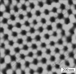
Fig.1 AFM photograph of AAO template
Fig.2 shows SEM images of the CuO nanowires grown in the AAO template. These photographs show that the nanowires are uniformly distributed, highly ordered, parallel to each other. Fig.2(a) shows planforms from which we can find several clusters of nanowires. The clusters can result from the situation in which the nanowires are uncovered from the framework of the AAO template but freestanding incompletely. When the top alumina of the AAO template is dissolved away, the nanowires embedded in the template release gradually and incline to agglutinate together. It is conceivable that the surface energy of the nanowires causes this interesting phenomenon. Fig.2(a) also shows that the CuO nanowires are abundant, uniform and highly ordered in large area. Fig.2(b) reveals a cross-section where the alumina matrix of the AAO template has been partially dissolved away. It can be seen that the nanowires deposited inside the nanochannel of the AAO template are parallel, tidily aligned and uniformly distributed. It is correlative to that the AAO template has an array of densely parallel nanoholes arranged in a hexagonal fashion. We can see that these nanowires have a fiber-brush aspect. From these figures, the CuO nanowire arrays can be produced in large areas within the pores of the AAO template. At the same time, it also can be estimated that the length of CuO nanowires is about 50 μm, which is corresponding with the thickness of the AAO template. The outside diameters of these nanowires are about 70 nm, which are equivalent to the pore diameter of the template membrane.
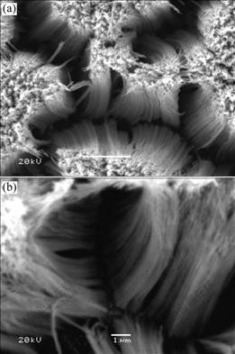
Fig.2 SEM images of CuO nanowires with AAO template partly dissolved: (a) Whole morphology of CuO/AAO composite; (b) CuO stripping from CuO/AAO composite
TEM images of CuO nanowires formed within the AAO template are shown in Fig.3. Fig.3(a) shows several CuO nanowires, in which some of these nanowires cross and overlap with each other. This image also shows that the diameter of CuO nanowires is about 70 nm, which approximately equals to those of the nanochannels of the employed AAO template. Although the length of nanowires is much less than 50 μm, it does not mean that the nanowires are only so short, because during the preparation of samples for TEM observation, the nanowires are easily broken by the ultrasonic stirring. These nanowires are uniformly distributed, which indicates that the alumina matrix is dissolved completely. In Fig.3(b) there is only a single one, the image shows that these nanowires are, in fact, microporous, resulting in a large surface area. Longer sintering time (up to 18 h) does not remove this microporosity[19]. The corresponding electron diffraction pattern shows continuous rings that are indexed to monoclinic CuO (insert of Fig.3(b)). The rings are sharp and continuous, which shows that although the nanowires are highly crystalline, they are not single crystals, and the various crystalline domains show no preferred orientation.

Fig.3 TEM image of dispersed CuO nanowires (a) and single CuO nanowires and corresponding selected area diffraction pattern (b) of nanowires
3.2 XRD analysis
Fig.4 shows XRD pattern of CuO nanowires. Although the background diffraction peaks of the Al2O3 template exist, the major diffraction peaks of CuO are observed. Four observed peaks with 2θ values of 35.57?, 38.75?, 49.01?, 66.44? and 67.92? correspond to diffraction from the  (111),
 and (220) planes of crystalline CuO, respectively. The reason for weaker diffraction peaks of CuO is the relatively small quantity of CuO in the template and the lack of CuO on the surface of the template. The XRD results not only reveal that the nanowires of CuO are crystalline as anticipated from the annealing temperatures, but also show no additional impurity diffraction from cubic Cu2O, indicating the phase purity of these nanowires[20].
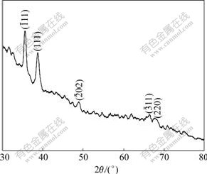
Fig.4 XRD pattern of CuO/alumina composite membrane
3.3 XPS analysis
Fig.5(a) shows XPS data for the CuO nanowires. The chemical composition of CuO nanowires (within the AAO template for a CuO/AAO composite) is obtained by XPS measurements. In order to see clear data, the AAO is partly removed. The C1s peak lies at 297.4 eV, which should be corrected to 285.0 eV. All the other peaks are corrected accordingly. No peaks of other elements except C, Cu and O are observed in the picture, indicating the high purity of the product. In the high-resolution XPS spectra (Figs.5(b) and (c)) of the as-prepared CuO nanowires, the Cu 2p3/2 and Cu 2p1/2 peaks lie at 933.7 eV and 953.6eV with a satellite feature respectively, the broad peak that lies at 530.9 eV is assigned to O 1s. No impurity peaks are observed in the XPS results for CuO, and this is in accordance with the XRD analysis.
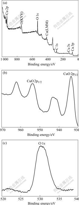
Fig.5 XPS spectra of CuO/alumina composite membrane wide spectrum (a), high-resolution Cu 2p (b) and high-resolution O1s (c)
References
[1] SHYUE J J, PADTURE N P. Template-directed, near-ambient synthesis of Au-TiO2-Au heterojunction nanowires mediated by self-assembled monolayers (SAMs)[J]. Materials Letters, 2007, 61(1): 182-185.
[2] WU R J, SUN Y L, LIN C C, CHEN W H, MURTHY C. Composite of TiO2 nanowires and Nafion as humidity sensor material[J]. Sensors and Actuators B: Chemical, 2006, 115(1): 198-204.
[3] ZHOU Shao-min. Fabrication and optical properties of Sb-doped CdS nanowires [J]. Materials Letters, 2007, 21(1): 119-122.
[4] WANG Zen, LI Hu-lin. Highly ordered zinc oxide nanotubular synthesized within the anodic aluminum oxide template [J]. Appl Phys A, 2002, 74: 201-203.
[5] BUDAK S, MIAO G X, OZDEMIR M, CHETRY K B, GUPTA A.Growth and characterization of single crystalline tin oxide (SnO2) nanowires [J].Journal of Crystal Growth, 2006, 2: 405-411.
[6] HE Yong-jun. A novel solid-stabilized emulsion approach to CuO nanostructured microspheres [J]. Materials Research Bulletin, 2007, 42(1): 190-195.
[7] UMBRAJKAR S M, SCHOENITZ M, DREIZIN E L. Exothermic reactions in Al-CuO nanocomposites [J]. Thermochimica Acta, 2006, 451: 34-43.
[8] NORMAN M R, FREEMAN A. Model supercell local density calculations of the 3d excitation spectra in NiO [J]. J Phys Rev B, 1986, 33: 8896-8898.
[9] SUKHORUKOV Y P, LOSHKAREVA N N, TUGUSHEV S N. Great magnetic linear dichroism in HgCr2Se4 and construction of an IR modulator based on it (great MLD in HgCr2Se4) [J]. J Magn Magn Mater, 1996, 159: 342-344.
[10] REITZ J B, SOLOMON E I. Propylene oxidation on copper oxide surfaces: Electronic and geometric contributions to reactivity and selectivity [J]. J Am Chem Soc, 1998, 120: 11467-11458.
[11] ISHIHARA T, HIGUCHI M, TAKAGI T, ITO M, NISHIGUCHI H, TAKITA T. Preparation of CuO thin films on porous BaTiO3 by self-assembled multibilayer film formation and application as a CO2 sensor [J]. J Mater Chem, 1998, 8: 2037-2042.
[12] JIANG Xu-chuan, HERRICKS T S, XIA You-nan. CuO nanowires can be synthesized by heating copper substrates in air [J]. Nano Lett, 2002, 2(12): 1333-1338.
[13] WANG W Z, WANG G H, WANG X S. Synthesis and characterization of Cu2O nanowires by a novel reduction route [J]. Adv Mater, 2002,14: 67-69.
[14] WANG Su-hua, HUANG Qun-jian, WEN Xiao-gang, LI Xiao-yuan, YANG Shi-he. Thermal oxidation of Cu2S nanowires: A template method for the fabrication of mesoscopic CuxO (x=1, 2) wires [J]. Phys Chem Chem Phys, 2002, 4: 3425-3429.
[15] MIAO Zheng, XU Dong-sheng, OUYANG Jian-hua, GUO Guo-lin, ZHAO Xin-sheng, TANG You-qi. Electrochemically induced sol-gel preparation of single- crystalline TiO2 nanowires [J]. Nano Lett, 2002, 2(7): 717-720.
[16] CEPAK V M, MARTIN C R. Preparation of polym eric micro-and nanostructures using a template-based deposition method [J]. Chem Mater, 1999, 11: 1363-1367.
[17] CHENG B, SAMULSKI E T. Fabrication and characterization of nanotubular semiconductor oxides In2O3 and Ga2O3 [J]. J Mater Chem, 2001, 11: 2901-2902.
[18] HUBER C A, HUBER T E, SADOQI M, LUBIN J A, MANALIS S, PRATER C B. Nanowire array composites [J]. Science, 1994, 263: 800-802.
[19] LAKSHMI B B, PATRISSI C J, MARTIN C R. Sol-gel template synthesis of semiconductor oxides micro-and nano-structures [J]. Chem Mater, 1997, 9: 2544-2548.
[20] ZHOU Ying-ke, LI Hu-lin. Sol-gel template synthesis and structural properties of a highly ordered LiNi0.5Mn0.5O2 nanowire array [J]. J Mater Chem, 2002, 12: 681-686.
Foundation item: Project(200623) supported by the Science Foundation of Shenzhen University, China
Corresponding author: SU Yi-kun; Tel: +86-755-26538536; E-mail: yikun@szu.edu.cn
(Edited by HE Xue-feng)

