Trans. Nonferrous Met. Soc. China 25(2015) 832-837
Electroplating mechanism of nanocrystalline NdFeB film
Zhong-nian YANG1,2, Cui WANG2, Yan ZHANG1, Yan XIE1
1. Department of Chemical Engineering, Binzhou University, Binzhou 256603, China;
2. College of Chemistry, Chemical Engineering and Materials Science, Shandong Normal University, Ji’nan 250014, China
Received 10 February 2014; accepted 20 January 2015
Abstract: Nanocrystalline NdFeB film was fabricated onto the copper substrate through direct current electroplating method, and characterized by scanning electron microscope (SEM) coupled with energy dispersive X-ray spectroscope (EDS), vibrating sample magnetometer and potentiodynamic polarization techniques. The initial electroplating behavior was investigated by cyclic voltammetry (CV) and electrochemical impedance spectroscopy (EIS) techniques. Results revealed that the corrosion resistance of the NdFeB film was better than that of the traditional sintered NdFeB magnet. The depositing process of the NdFeB film followed the three-dimensional nucleation and subsequent grain growth mechanism, and was controlled by charger transfer. With the increase of the negative potential bias, the deposition mechanism of NdFeB film changed from heterogeneous to homogeneous nucleation/growth, which consequently resulted in the decrease of charge-transfer-resistance.
Key words: NdFeB film; electrodeposition; corrosion; magnetic property
1 Introduction
The development of rare earth permanent magnet materials has experienced three stages according to their performance since 1980s [1-3]: the appearance of SmCo5 (1-5 samarium cobalt alloy), the occurrence of Sm2Co17 (2-17 samarium cobalt alloy) and the invention of NdFeB. Because of the superior performance of permanent magnet NdFeB, such as high saturation magnetization, high coercive force, large magnetic energy product (the theoretical magnetic energy product is as high as 512 kJ/m3 [4-6], NdFeB has been considered as an ideal substitution for samarium cobalt permanent magnet [7], which has been widely used in automobiles, household appliances and other fields. However, the poor anti-corrosion performance of the traditional sintered polycrystalline NdFeB [8,9] limits its application in many environments.
Nowadays, many techniques have been proposed to increase the corrosion resistance, of which the common ground is to form a layer of protective film onto the surface of NdFeB [1]. Among them, electrodeposition is an attractive method for film preparation and possesses many advantages, such as low processing temperature, normal handling pressure and high purity of deposits. On the other hand, electrodeposition is also well known to be an important technique for fabricating nano-structured materials with high corrosion resistance [10-12]. Therefore, it is rational to deduce that the electrodeposited NdFeB should possess good anti- corrosion performance.
During the electroplating process of materials, the electrocrystallization nucleation/growth mechanism has great influence on the structure and performance of coatings [13-15]. Thus, it is particularly important to research their initial electroplating behavior.
The aim of this work is to fabricate NdFeB nanocrystalline film onto copper substrate with direct current deposition technique, especially investigate its initial electro-crystallization behaviors by cyclic voltammetry (CV) and electrochemical impedance spectroscopy (EIS) techniques. Furthermore, its corrosion behavior was also studied by EIS and potentiodynamic polarization tests.
2 Experimental
The nanocrystalline NdFeB film was electro- deposited onto copper substrates from the electrolyte (Tables 1 and 2), which was prepared with AR grade reagents and double-distilled water. The pH value of solution was adjusted to 3.15-3.30 with diluted HCl and NaOH solution. The experimental temperature was controlled at (50±1) °C by the thermostat water tank.
Table 1 Composition of electroplating solution
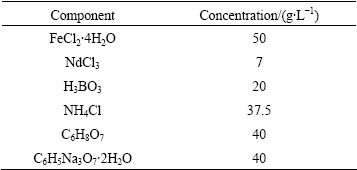
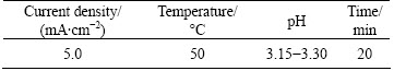
Table 2 Electroplating conditions for fabricating NdFeB film
ZF-9 constant voltage/current meter (China) was used to provide the electroplating DC current. The copper cylinder was used as the cathode, and a large bright platinum foil was used as the anode. Before each experiment, the exposed surface of the copper working electrode was polished to mirror using 2.5 mm diamond paste, rinsed with acetone and double-distilled water and then dried in air.
All electrochemical measurements were carried out in a conventional three-electrode configuration at (25±1) °C. A saturated calomel electrode (SCE) connected through a salt bridge and a large platinum foil served as reference and counter electrode, respectively. In this work, all potentials were referred to SCE unless otherwise stated. EIS measurements were taken at different cathodic potential biases (relative to the open circuit potential, OCP) with PARSTAT2273 electro- chemical workstation over the frequency range from 10000 to 0.005 Hz with the voltage amplitude of 10 mV. Z-view software was used to analyze the EIS data. CV and the potentiodynamic polarization tests were performed with a commercial Model 660C electrochemical workstation (China). The sweep rate of potentiodynamic polarization is 1 mV/s in the potential range from OCP -0.3 V to OCP 0.3 V, while the sweep rates of CV are 2, 5 and 10 mV/s respectively. Before all tests,the bath solution was hold still for 10 min and the working electrode was polished as mentioned above.
The surface morphology of the film was characterized using SEM (SUPRATM 55) and the film composition was analyzed with Oxford energy detective spectrometer (EDS). The crystallographic structure of the films was identified by an X-ray diffractometer (XRD, Panalytical, X’pert PRO) by employing Cu Kα radiation as the incident radiation.
The magnetic properties were analyzed with vibrating sample magnetometer (VSM, VSM7407, US), which possessed a measurement accuracy of as high as 5×10⁻¹⁰ A・m.
3 Results and discussion
3.1 Characters of obtained NdFeB film
The SEM images of the obtained NdFeB films are shown in Fig. 1. It can be seen that the film surface was relatively smooth (see Fig. 1(a)) and possessed nanocrystalline structure (see Fig. 1(b)). The maximum grain diameter was less than 100 nm. Figure 2 shows the energy dispersive X-ray spectroscopy (EDS) analysis result of the film. It can be observed that the film contained Fe, Nd and B. The peaks observed for C and O were attributed to contamination caused by air exposure. The Cu peak was derived from the substrate.
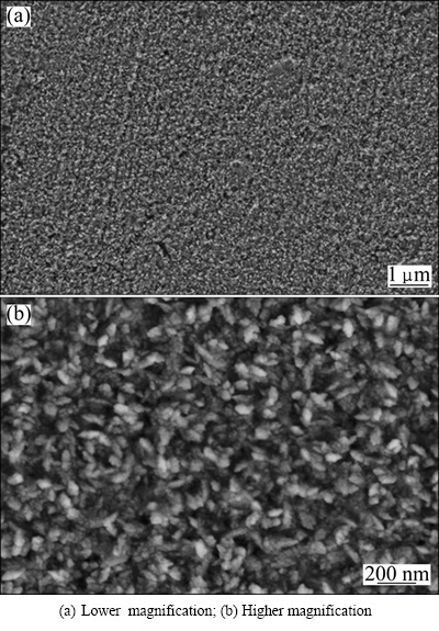
Fig. 1 SEM images of nanostructured NdFeB film

Fig. 2 EDS result for as-prepared NdFeB film
The XRD pattern of the film is displayed in Fig. 3. The result indicated that there was a sharp peak which corresponded to the α-Fe [16]. No diffraction peaks related to NdFeB could be observed since there was only little amount of NdFeB in the prepared film.
From the XRD pattern, the average of crystallites was calculated using the Debye-Scherrer equation:
D=kλ/(βcos θ) (1)
where D is the grain size, k=0.89, λ is the wavelength of the X-rays (λ=0.1542 nm), β is the full width at half maximum and θ is the half diffraction angle of crystal orientation peak. The calculated result indicated that the average size of crystallites was 1.15 nm. Therefore, the XRD result confirmed that the film possessed nanocrystalline structures.
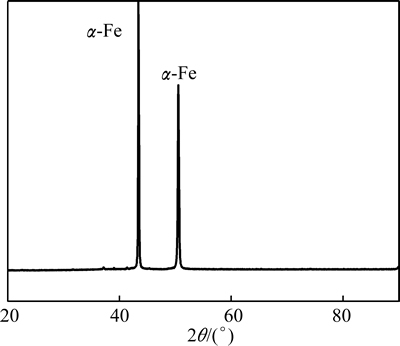
Fig. 3 XRD pattern of NdFeB film
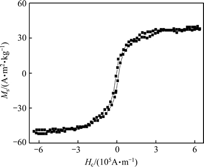
Fig. 4 Magnetic hysteresis loop of nanocrystalline NdFeB film
The film magnetic properties of main interest are the saturation flux density Ms and the coercivity Hc. Figure 4 shows that the Ms and Hc of the obtained nano-crystalline NdFeB film were 38.67 A・m2/kg and 1457.6 A/m, respectively, suggesting it may be a good soft magnetic material.
Figure 5 shows the anti-corrosion properties of the obtained NdFeB film and the traditional sintered NdFeB. It can be seen that the corrosion potential of the obtained NdFeB film was much positive than that of the traditional sintered NdFeB, while the corrosion current of the former was much smaller than that of the latter. The results indicated that the obtained NdFeB film possessed higher corrosion resistance than the traditional sintered NdFeB.

Fig. 5 Potentiodynamic polarization curves of obtained NdFeB film and traditional sintered NdFeB
3.2 Electroplating behavior of NdFeB film
The electroplating behavior of NdFeB film was investigated using cyclic voltammetry at different sweep rates of 2, 5 and 10 mV/s. The cyclic voltammetry sweep always initiated negatively from OCP to -1.7 V. It is apparent that the CV curves were much similar (Fig. 6). In the cathodic branch, the current density sharply increased at about -0.9 V, which can be attributed to the reduction of Fe and Nd. In the anodic branch, an anodic peak appeared at about -0.28 V, which maybe corresponded to the oxidation of deposit. It can also be seen that there was a typical current loop in the cathodic branch of the voltammogram, which indicated that the co-deposition of NdFeB film followed the three dimensional (3-D) nucleation/grain growth mechanism [17-20]. Due to the phenomenon of hydrogen evolution, the current possessed some fluctuations during the potential less than -1.2 V [21].

Fig. 6 Cyclic voltammetry curves of NdFeB film in electroplating solutions
Figure 7 shows the EIS plots in the electroplating process at different cathodic potential biases (vs OCP), including Nyquist and Bode plots. It can be seen that all plots were composed of only one high-frequency capacitive loop caused by the electrochemical process. All centers of the high-frequency capacitive circles were below the real axis, which indicated that the electroplating process of nanocrystalline NdFeB film was under activation control. The low frequency data of EIS plots were much discrete due to the hydrogen evolution, which occurred concurrently with the co-depositing of NdFeB and can be proved by the observation of some bubbles on the substrate, especially at high cathodic potential bias. The effect of H2 can be ignored under low deposition potential, while at high potential bias, it may cause the instability on the electrode surface [22], resulting in the discreteness in the impedance spectra.
Black film was observed when the potential bias was lower than -0.88 V, which may be related to the co-electrodeposition process of Nd and Fe. This phenomenon agreed well with the results of CV measurements as mentioned above. With the increase of the negative potential bias, the radius of the high frequency capacitive loop (related to the charge transfer resistance) decreased rapidly, and the corresponding phase angle moved to a higher frequency range, indicating that the rate of charge transfer process increased greatly.
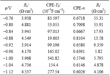
According to the above analysis, the electrochemical equivalent circuit model is shown in Fig. 8. In Fig. 8, Rs is the electrolyte resistance, Rt is the charge transfer resistance, and CPE1 is a constant phase angle element associated with the electric double layer capacitance. The fitted parameters are summarized in Table 3.
It can be seen from Table 3 that the electrolyte resistance basically remained unchanged. With the increase of negative potential bias, Rt decreased gradually. In the case of low cathodic potential bias, the nucleation and growth reaction mainly occurred on the heterogeneous copper matrix, the activation energy was large and the Rt was high as well. With the increase of the cathodic potential bias, the Fermi level of the matrix increased [9,23], and the number of the nucleation active sites on the surface also increased, therefore the electroplating reaction transferred from heterogeneous nucleation/growth gradually into homogeneous nucleation/growth and resulted in the decrease of Rt.
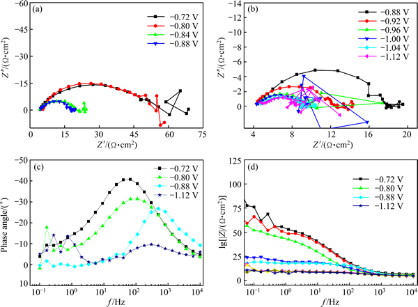
Fig. 7 Impedance spectra recorded during NdFeB deposition at different cathodic potential biases

Fig. 8 Electrochemical equivalent circuit model for NdFeB coating deposition
Table 3 Parameters of equivalent circuit during NdFeB deposition at different potential biases
The influence of the cathodic potential bias or the overpotential (η) on Rt is plotted in Fig. 9. It can be seen that Rt decreased with η exponentially. According to the secondary thermal dynamic law, the electrochemical activation energy (ΔH*) of unit electrode process O+ ne→ R is
 (2)
(2)
where O and R represent the oxidation and reduction state of the electrochemically reactive species, respectively; ΔH and ΔG* are the pure thermochemical activation energy and free enthalpy of the unite electrode reaction O+ne→R respectively; F is the Faradaic constant and η is the overpotential.
Therefore, based on the Arrhenius equation, the electrochemical reaction rate constant κ of the unite electrode reaction O+ne→R can be obtained.
 (3)
(3)
where A is the pre-exponential factor, T is the thermodynamic temperature and R is the mole gas constant. At a constant electroplating bath temperature T and under ambient pressure, ΔH is also a constant. Therefore, the electrochemical reaction rate constant κ of the unit electrode reaction O+ne→R increased exponentially with the applied potential bias (or overpotential η), which caused the exponential decay of Rt with the applied potential bias.
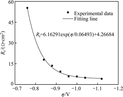
Fig. 9 Variation of Rt with applied cathodic potential bias η
4 Conclusions
1) Nanocrystalline NdFeB film with both soft magnetic properties and high corrosion resistance was prepared onto the copper electrode through direct current electroplating method. The surface of the film was sufficiently smooth with an average grain diameter of about 50 nm.
2) The co-deposition of NdFeB film followed the 3-D nucleation/grain growth mechanism. With the increase of negative potential bias, the type of the reaction changed from heterogeneous nucleation/growth gradually to homogeneous nucleation/growth, and the charge transfer resistance decreased exponentially.
References
[1] MA Cheng-bin, CAO Fa-he, ZHANG Zhao, ZHANG Jian-qing. Electrodeposition of amorphous Ni-P coatings onto Nd-Fe-B permanent magnet substrates [J]. Applied Surface Science, 2006, 253(4): 2251-2256.
[2] ALI A, AHMAD A, DEEN K M. Multilayer ceramic coating for impeding corrosion of sintered NdFeB magnets [J]. Journal of Rare Earths, 2009, 27(6): 1003-1007.
[3] SONG Lai-zhou, YANG Zhi-yong. Corrosion resistance of sintered NdFeB permanent magnet with Ni-P/TiO2 composite film [J]. Journal of Iron and Steel Research International, 2009, 16(3): 89-94.
[4] CHEN Bi-qing, WANG Jian-chao, GUO Cheng-yu. Preparation of rare earth magnetic materials and mechanism of electrodeposition [J]. Journal of Qinghai Normal University, 2011(1): 30-31. (in Chinese)
[5] YAN Wen-long, YAN Shi-hong, YU Dun-bo, XU Jing, YANG Hong-chuan, HU Quan-xia, LU Yang. Development and application of NdFeB status [J]. Metallic Functional Materials, 2008, 15(6): 33-37. (in Chinese)
[6] LI Qing, YANG Xiao-kui, ZHANG Liang, WANG Ju-ping, CHEN Bo. Corrosion resistance and mechanical properties of pulse electrodeposited Ni-TiO2 composite coating for sintered NdFeB magnet [J]. Journal of Alloys and Compounds, 2009, 482(1-2): 339-344.
[7] KOLCHUGINA N B. Distillation purification of cerium-group rare-earth metals for fundamental research and design of new materials [J]. Inorganic Materials: Applied Research, 2012, 3(2): 75-80.
[8] WEI Cheng-fu, TANG Jie, YANG Li-rong, ZHAO Dao-wen, LIN Hong, DENG Cheng-xian. Research and application of NdFeB progress [J]. Rare Metals and Cemented Carbides, 2010, 38(1): 47-49. (in Chinese)
[9] CHEN E, PENG Kun, ZHU Jia-jun, LI De-yi, ZHOU Ling-ping. Effect of Al coating on corrosion resistance of sintered NdFeB magnet [J]. Transactions of Nonferrous Metal of Society of China, 2014, 24(9): 2864-2869.
[10] WANG Sheng-gang, SHEN Chang-bin, LONG Kang, ZHANG Tao, WANG Fu-hui, ZHANG Zhi-dong. The electrochemical corrosion of bulk nanocrystalline ingot iron in acidic sulfate solution [J]. The Journal of Physical Chemistry B, 2006, 110(1): 377-382.
[11] WANG Sheng-gang, SHEN Chang-bin, LONG Kang, YANG Huai-yu, WANG Fu-hui, ZHANG Zhi-dong. Preparation and electrochemical corrosion behavior of bulk nanocrystalline ingot iron in HCl acid solution [J]. The Journal of Physical Chemistry B, 2005, 109(7): 2499-2503.
[12] JUNG H, ALFANTAZI A. An electrochemical impedance spectroscopy and polarization study of nanocrystalline Co and Co-P alloy in 0.1 M H2SO4 solution [J]. Electrochimica Acta, 2006, 51(8-9): 1806-1814.
[13] MIRANDA-HERNANDEZ M, PALOMAR-PARDAVE M, BATINA N, GONZALEZ I. Identification of different silver nucleation processes on vitreous carbon surfaces from an ammonia electrolytic bath [J]. Journal of Electroanalytical Chemistry, 1998, 443(1): 81-93.
[14] PALOMAR-PARDAVE M, MIRANDA-HERNANDEZ M, GONZALEZ I, BATINA N. Detailed characterization of potentiostatic current transients with 2D-2D and 2D-3D nucleation transitions [J]. Surface Science, 1998, 399(1): 80-95.
[15] BARRERA E, PALOMAR-PARDAVE M, BATINA N, GONZALEZ I. Formation mechanisms and characterization of black and white cobalt electrdeposition onto stainless steel [J]. Journal of Electrochemical Society, 2000, 147(5): 1787-1796.
[16] GAO Da-qiang, FU Jun-li, XU Yan, XUE Da-sheng. Preparation and magnetic properties of Nd5Fe95-xBx nanowire arrays [J]. Materials Letters, 2008, 62(17-18): 3070-3072.
[17] JAYA S, PRASADA RAO T, PRABHAKARA RAO G. Electrochemical phase formation (I): The electrodeposition of copper on glassy carbon [J]. Electrochimica Acta, 1986, 31(3): 343-348.
[18] PALOMAR-PARDAVE M, GONZALEZ I, BATINA N. New insights into evaluation of kinetic parameters for potentiostatic metal deposition with under potential and over potential deposition process [J]. The Journal of Physical Chemistry B, 2000, 104(15): 3545-3555.
[19] GRUJICIC D, PESIC B. Electrodeposition of copper: The nucleation mechanisms [J]. Electrochimica Acta, 2002, 47(18): 2901-2912.
[20] MENDOZA-HUIZAR L H, ROBLES J, PALOMAR-PARDAVE M. Nucleation and growth of cobalt onto different substrates: Part II. The upd-opd transition onto a gold electrode [J]. Journal of Electroanalytical Chemistry, 2003, 545(27): 39-45.
[21] SONG Li-Xiao, ZHANG Zhao, ZHANG Jian-qing, CAO Chu-nan. Electroplating mechanism of nanostructured black Ni films [J]. Acta Metallurgica Sinica, 2011, 47(1): 123-127. (in Chinese)
[22] WANG Qiu-ping. The electrochemical preparation of the nanocrystalline CoNiFe soft magnetic thin films and the research of its structure and performance [D]. Hangzhou: Zhejiang University, 2010: 56-60. (in Chinese)
[23] JUNEGHANI M A, FARZAM H, ZOHDIRAD H. Wear and corrosion resistance and electroplating characteristics of electrodeposited Cr-SiC nano-composite coatings [J]. Transactions of Nonferrous Metals Society of China, 2013, 23(7): 1993-2001.
纳米晶NdFeB薄膜的电沉积机理
杨仲年1,2,王 萃2,张 岩1,谢 彦1
1. 滨州学院 化学工程系,滨州 256603;
2. 山东师范大学 化学化工与材料科学学院,济南 250014
摘 要:采用直流电沉积法在铜基体表面制备纳米晶NdFeB薄膜。利用扫描电镜、能谱、振动样品磁强计和动电位极化技术对样品进行表征。采用循环伏安和电化学阻抗技术对NdFeB膜电沉积初期的电化学行为进行研究。结果表明,电沉积制备的NdFeB膜的耐蚀性能优于传统烧结法制备的NdFeB膜的耐蚀性能。纳米晶NdFeB磁性薄膜的电沉积初期遵循3D瞬时成核/生长机制,电荷转移为速控步骤。随着外加沉积电位的增大,异质成核/生长逐渐转变为同质成核/生长,因此电沉积过程的电荷转移电阻减小。
关键词:NdFeB薄膜;电沉积;腐蚀;磁性能
(Edited by Xiang-qun LI)
Foundation item: Project (2008BS04030) supported by Research Award Fund for Outstanding Young Scientists in Shandong Province, China
Corresponding author: Zhong-nian YANG; Tel: +86-15963078773; E-mail: yangzhongnian@126.com
DOI: 10.1016/S1003-6326(15)63670-6

