J. Cent. South Univ. Technol. (2011) 18: 2031-2035
DOI: 10.1007/s11771-011-0938-5
Improved direct power injection model of 16-bit microcontroller for electromagnetic immunity prediction
GAO Xue-lian(��ѩ��), TIAN Cong-ying(���ӱ), LAO Li-yuan(������),
CHEN Yin-hong(������), CHEN Yan-yu(������)
School of Electrical and Electronic Engineering, North China Electric Power University, Beijing 102206, China
? Central South University Press and Springer-Verlag Berlin Heidelberg 2011
Abstract: To promote the modeling standardization process of the integrated circuits, an improved electrical simulation model for a direct power injection (DPI) setup which was used to measure the conducted immunity of a 16-bit microcontroller to radio frequency aggression was investigated. Based on the existing model of the same microcontroller, the PDN module was modified by adding the core, PLL and A/D network models, which could reflect the actual electric distribution situation within the microcontroller more accurately. By comparing the simulation results with the measurement results, the effectiveness of the modified model can be improved to 500 MHz, and its uncertainty is within ��1.8 dB (��2 dB is acceptable). Then, to improve the simulation accuracy of the complete model in the high frequency range, the I/O model which contained the dynamic and nonlinear characteristics reflecting the variation of the internal impedance of the microcontroller with increasing the frequency of the external noise was introduced. By comparing the simulation results with the measurement results, the effectiveness of the second modified model can be improved up to 1.4 GHz with the uncertainty of ��1.8 dB. Thus, a conclusion can be reached that the proposed model can be applied to a much wider frequency range with a smaller uncertainty than the latest model of the similar type. Furthermore, associated with the electromagnetic emission testing platform model, the PDN module can also be used to predict the electromagnetic conducted and radiated emission characteristics. This modeling method can also be applied to other integrated circuits, which is very helpful to the standardization of the IC electromagnetic compatibility (EMC) modeling process.
Key words: electromagnetic immunity; microcontroller; direct power injection; passive distribution network
1 Introduction
The electromagnetic compatibility problems at IC level cannot be ignored in recent years. On one hand, ICs are more and more susceptible to higher radio frequency interference (RFI) with the increase of the integration density and the rise of the IC operating frequency. On the other hand, the supply voltages become lower and lower, which reduces the static noise margin of electrical signals and thus increases the IC susceptibility to RFI. With the multiplication of powerful parasitic sources, such as mobile phones, high speed networks, and wireless systems, which can affect the behavior of circuits, immunity to RFI is becoming a major concern for integrated circuits [1-2]. Under this situation, both IC vendors and customers have the potential demand to predict if an IC can meet the EMC standards at an early stage of its design cycle.
In the field of IC immunity, a few dedicated simulation methodologies or models have been proposed [3-6]. The approaches to immunity simulation of an IC are much more complex than those to emission simulation because it is hard to observe and evaluate the real impact of external perturbations on complex ICs and to get reasonable results from time-consuming iterative simulations [7]. In the recent years, a conducted immunity model for a microcontroller has been proposed by the French workgroup [5], which could simulate the conducted immunity of the I/O ports accurately under the radio frequency interference below 900 MHz. However, large error appeared when the simulation reached a higher frequency.
To solve these problems mentioned above, the model in Ref.[5] was improved in this work. First, based on the existing model of the same microcontroller, the PDN module was modified by adding the core, PLL and A/D network models, which could reflect the actual electric distribution situation within the microcontroller more accurately. Besides, it has been proved that the PDN module could also predict the input impedance, the
electromagnetic conducted and radiated emission characteristics of the microcontroller effectively [8], and the extraction method of the PDN was conductive to the standardization progress of the EMC modeling for IC. Second, to reflect the variation of the internal impedance of the microcontroller with increasing the frequency of the external noise, the I/O module considered the dynamic and non-linear factors.
The accuracy is much higher by using this proposed model instead of IC element in PCB overall simulation structure than the IBIS model. From the viewpoint of semiconductor manufacturers, they can provide customers with a non-confidential model and get an EMC guideline for the IC circuit designers. As for users, the simulation of the electromagnetic compatibility of an IC completed by discrete component model is much better than that finished by IBIS in high frequency. And for both of the semiconductor manufacturers and users, they all wish to get a unified EMC model which can simulate the electromagnetic emission and immunity characteristics effectively at the same time. So, the immunity modeling process of a special 16-bit microcontroller will be introduced.
2 Test chip and DPI method
The research was focused on a commercial chip, Freescale Semiconductor 16-bit microcontroller MC9S12XDP512. This TQFP 144-pin IC has eight pairs of power and ground pins to supply power to the Input/ Output (I/O) ports, the Analog-to-Digital (A/D) converter, the oscillator, the Phase-Locked-Loop (PLL), and the digital core. The digital core is fed by the internal voltage regulator which is supplied by VDDR1/VSSR1 and VDDR2/VSSR2 pins. The VDD1 and VDD2 power supply pins are connected to the internal 2.5 V core voltage, and two 100 nF on-board CMS capacitances are connected through VDD1/VSS1 and VDD2/VSS2 pins. Some I/O ports such as J, K, M, P, S and T are fed by VDDX1/VSSX1 and VDDX2/VSSX2 pins while the others are supplied by VDDR1/VSSR1 and VDDR2/ VSSR2 pins.
An important standard test method used to characterize the immunity of integrated circuits is the direct power injection [9] which applies a conducted RF interference to the I/O pin under test via a 6.8 nF coupling capacitance. The RF disturbances are generated from an RF generator followed by a 10 W power amplifier. In this approach, one of I/Os named PT3 was configured as the test pin for its conducted immunity characteristics of the microcontroller. When the output voltage reached the failure limit, the related RF disturbance was monitored through the directional coupler by measuring the forward power as the immunity threshold.
3 Immunity simulation environment and methodology
To simulate the immunity threshold of the microcontroller, a free software named IC-EMC 2.0 [10], developed at LESIA-Toulouse, with an analog simulator Winspice [11] was used in the simulation process. IC-EMC 2.0 is a professional EMC simulation software that can accurately extract the relevant electromagnetic emission, immunity and other EMC characteristics in IC level.
Figure 1 shows the general flow for the immunity simulation of the microcontroller. Before the automatic immunity simulation process, users had to configure the amplitude sweeping, frequency sweeping and the transient simulation length of the RF disturbances, then ran Winspice. At the end of the simulation, forward powers required to induce a failure were extracted at each frequency. The measured and extracted forward powers could be compared in the immunity window of IC-EMC 2.0.
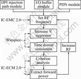
Fig.1 Immunity simulation flow
4 Improved conducted immunity model for microcontroller
The overall structure of the conducted immunity model is composed of three segments: the DPI injection path module, the I/O module and the PDN module.
4.1 DPI injection path module
The DPI injection path has a direct impact on the immunity of the microcontroller, whose model includes the SMA connector, the DPI capacitor, the PCB track, and the lead and bonding of the package (Fig.2). The package model structure and parameters were set according to the IBIS model structure and its data-sheet. The DPI injection path module was the same as the one illustrated in Ref.[5], and the validation of the module has been demonstrated in Ref.[12].
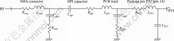
Fig.2 DPI injection path module
4.2 I/O module
Three components are essential to the I/Os immunity model, as described in Ref.[5]: the input equivalent capacitance, the electrostatic discharge (ESD) protection diodes and the input buffer models [13]. The input equivalent capacity was set to 6 pF according to the IBIS file, and could also be evaluated by the measurement of the input impedance of the coupling path. The power clamp diode models and the ground clamp diode models were extracted from their I(V) characteristic curves given by the IBIS file of S12x. Furthermore, the clamp diode information could be tested by using the Transmission Line Pulse (TLP) method, if it was not provided by the IBIS [14]. The input buffer aimed at converting the input voltage into a logic state. Actually, the buffer switching had an impact on the I/O immunity, but there was no information about it in the IBIS. In this approach, the input transfer function was tested by applying a triangular signal to the input buffer and observing the output state of the I/O, then the output voltage curves in time domain could be gotten at different frequencies. The result shows that the buffer is triggered synchronously with the action of ESD protection, and confirms the presence of a Schmitt trigger which has a hysteresis cycle of 0.5 V. A feedback loop could be used to simulate the hysteresis characteristics of the Schmitt trigger.
4.3 Passive distribution network module
Although the PDN module described in Ref.[5] with only the VDDX and VDDR network structures could fulfill the immunity simulation work, the simplified module could not predict the emission characteristics. So, the PDN module was unable to meet the EMC standardization needs. Based on the PDN module in Ref.[5], a more complex PDN structure with additive core, PLL and A/D networks was linked to the I/O module, which could reflect the actual electric distribution situation within the microcontroller more accurately. The improved PDN module described the major power network of the microcontroller, which consisted of the VDDR networks, the core, PLL, A/D networks, and the inter-block coupling model that reflected the parasitic substrate coupling between each block. The PDN parameters were computed from electrostatic formula and tuned to ?t with the measurement results such as the amplitude and phase matrixes of the S-parameter and the impedance matrixes between each power and ground pins [15]. In the model, some inductive coupling coef?cients were added to reflect the inductive coupling effect between adjacent leads, in which values were computed by the ?nite element method (FEM). Moreover, the improved PDN module could also simulate the S-parameters, impedance, electromagnetic conducted and radiated emission characteristics of the microcontroller with wonderful outcomes by comparing with the measurement results. Therefore, the application of this module is very useful for the EMC standardization process.
4.4 Complete model
A combination of different parts of the model is eventually carried out to predict the conducted immunity as shown in Fig.3. The simulation process was based on the same principle of the DPI configuration. The disturbance level was increased linearly at a given frequency during the simulation, which thanked for a sinusoidal programmable source. The output voltage of the I/O was selected to describe the immunity characteristics of the microcontroller, and its failure criterion was set to be 2.5 V, which meant that the output voltage exceeding this limit would cause a change of the logical state of the input I/O and would exhibit the error information at the output I/O simultaneously.
Figure 4 gives the comparison between measurement and simulation results of the impedance seen from the RF inject port, which shows a very close correlation between simulated curve and measured curve up to 2 GHz. Meanwhile, in Fig.5, a good agreement between measured and simulated immunity threshold results is obtained up to 500 MHz. At 850 MHz, the uncertainty even reaches ��6 dB. One of the reasons is that the internal impedance of the microcontroller varies with increasing the frequency dynamically and nonlinearly.
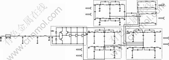
Fig.3 Complete model of microcontroller
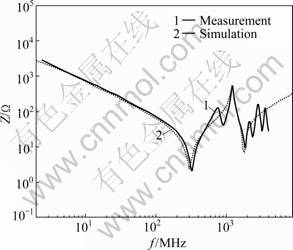
Fig.4 Comparison between measurement and simulation results of impedance
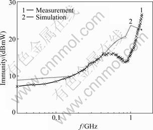
Fig.5 Comparison between measurement and simulation results of immunity threshold
5 Secondary modified immunity model for microcontroller
Experiments show that the input impedance of the I/O varies with the increasing frequency of RF noise dynamically and nonlinearly. To describe this phenomenon, two variable resistors Rvar1, Rvar2 and a capacitor Cadj are added between the power and ground path at the end of the I/O buffer model introduced in Ref.[5] as the dynamic and nonlinear factors (Fig.6). The values of the resistors Rvar1 and Rvar2 are dependent on the frequency of RF interference. The capacitor Cadj represents the capacitive coupling effect between I/O under test and the substrate of the microcontroller.
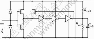
Fig.6 Modified I/O model with dynamic and nonlinear elements
Figure 7 presents the comparison between the measured and simulated immunity threshold given in terms of forward power. The simulation curve provides a good correlation with the measurement up to 1.4 GHz. The uncertainty of the simulation result is within ��1.8 dB over the whole frequency range. As errors do exist during the DPI immunity measurement process, and the discrete components used in the model cannot completely represent the actual physical construction of the microcontroller, a gap of ��2 dB is not a vital concern. Experiment results show that the consideration of the variation of the I/O input impedance with the external RF interference at different frequencies and the expansion of the PDN module can significantly improve the effectiveness of the model in high frequency band.
Furthermore, it must be pointed out that the current source can be added in the PDN module of the complete immunity model for the microcontroller to represent the internal activity of the core, which can be described in the form of formulas, graphics, documents and other formats. However, the software configured in this immunity measurement is very simple, in which the function is just to read the state of the I/O under test regularly and to copy the logic state to another I/O. Experiments show that not only the small action of the core but also the whole core network has an insignificant effect on the whole immunity simulation process, so they can be ignored in this modeling approach.
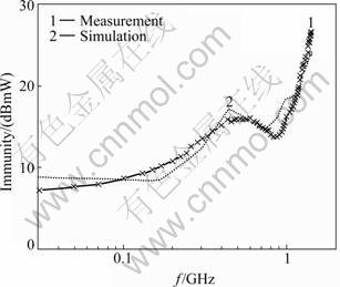
Fig.7 Comparison between measurement and simulation results of immunity threshold
6 Conclusions
1) According to an existing model of the international research work, an improved conducted immunity model with a modified PDN module is applied to a microcontroller, which is very useful in the standardization of the IC electromagnetic compatibility modeling process. This model is validated by the agreement of the simulation and measurement results up to 500 MHz with an acceptable uncertainty.
2) A secondary improved conducted immunity model is achieved by considering the dynamic and nonlinear factors which reflect the variation of the internal impedance of the microcontroller with increasing the frequency of the external noise. The simulation results prove that the improved model can well characterize the conducted immunity of the microcontroller up to 1.4 GHz with an acceptable uncertainty.
3) The conducted immunity model can be directly applied to the electromagnetic emission and immunity simulation in PCB level, and the simulation results can be used as a reference for chips choosing. This modeling method can also be applied to other integrated circuits, which is very helpful in the standardization of the IC electromagnetic compatibility modeling process.
References
[1] SKETOE J G. Integrated circuit electromagnetic immunity handbook [M]. Seattle: NASA, 2000: 64.
[2] BENDHIA S, RAMDANI M, SICARD E. Electromagnetic compatibility of integrated circuits��Techniques for low emission and immunity [M]. New York: Springer, 2006: 1.
[3] ICHIKAWA K. Simulation of integrated circuit immunity with LECCS model [C]// 17th International Zurich Symposium on Electromagnetic Compatibility. Singapore, 2006: 308-311.
[4] LENANT J L, RAMDANI M, PERDRIAU R, DRISSI M. EMC assessment at chip and PCB level: Use of the ICEM model for jitter analysis in an integrated PLL [J]. IEEE Trans on Electromagnetic Compatibility, 2007, 49: 182-191.
[5] BOYER A, BENDHIA S, SICARD E. Modelling of a direct power injection aggression on a 16 bit microcontroller input buffer [C]// EMC Compo 07. Torino, 2007: 35-39.
[6] SU T, UNGAR M, STEINECK T, WEIGEL R. Dynamic, nonlinear and passive model of microcontroller for immunity simulation [C]// Electromagnetic Compatibility and 19th International Zurich Symposium on Electromagnetic Compatibility. Singapore, 2008: 28- 31.
[7] RAMDANI M, SICARD E, BOYER A, BEN DHIA S, WHALEN J J, HUBING T, COENEN M and WADA O. The electromagnetic compatibility of integrated circuits��Past, present and future [J]. IEEE Trans on Electromagnetic Compatibility, 2009, 51: 78-100
[8] LABUSSI?RE C, BENDHIA S, SICARD E. Modeling the electromagnetic emission of a microcontroller using a single model [J]. IEEE Trans on Electromagnetic Compatibility, 2008, 50: 22-34.
[9] IEC 62132-4: Integrated circuits�Cmeasurement of electromagnetic immunity, 150 KHz to 1 GHz: Part 4. Direct RF power injection method [S]. International Electrotechnical Commission, Geneva: IEC, 2004.
[10] SICARD E, BOYER A. Software: Ic-emc2.0 [EB]. [2010-07-22]. http://www.ic-emc.org/
[11] Ousetech Ltd. Software: Winspice [EB]. [2010-07-22]. http:// www.winspice.com
[12] SICARD E, BOYER A. IC-EMC v2.0 user��s manual [M]. INSA Toulouse, 2009: 90.
[13] LAMOUREUX E. Research on the susceptibility of digital integrates circuits with high frequency aggressions [C]// INSA. 2006: 132. (in French)
[14] MALONEY T J, KHURANA N. Transmission line pulsing techniques for circuit modeling of ESD phenomena [C]// EOS/ESD Symposium Proceedings. Minneapolis, MN, 1985: 49-54.
[15] LABUSSI?RE C, SICARD E, LOCHOT C, BOUISSE G, TAO Jun-wu. Characterization and modeling of the supply network from an integrated circuit up to 12 GHz [C]// EMC Europe. Barcelona, 2006: 894-899.
(Edited by YANG Bing)
Foundation item: Project(2007dfa71250) supported by the International Science and Technology Cooperative Program of China; Project(20062250) supported by the Doctor Fund of North China Electric Power University, China
Received date: 2010-09-17; Accepted date: 2011-04-20
Corresponding author: GAO Xue-lian, PhD; Tel: +86-10-51971418; E-mail: xuelian_gao@ncepu.edu.cn

