˫�дſؽ������Cu-W��Ĥ��֯�ṹ���������ݱ�
��Դ�ڿ����й���ɫ����ѧ��(Ӣ�İ�)2012���11��
�������ߣ�����ƽ ������ �� �� ��ҿ� �� �� �� ��
����ҳ�룺2700 - 2706
�ؼ��ʣ�Cu-W��Ĥ������������Ǿ��ࣻ��״�ṹ�����ܶȣ�Vegard����
Key words��Cu-W thin film; sputtering deposition; amorphous phase; layer structure; solid solubility; Vegard law
ժ Ҫ������˫�дſؽ������Cu-W�Ͻ�Ĥ��ͨ��XRD��TEM��HRTEM�ȷ�������������Ĥ��֯�ṹ�����ݱ���ɡ��ڳ������ڣ�Cu-W��Ĥ�ʷǾ�̬�����ų������̵Ľ��У��ڽ������ӵĺ�����ѳ�����Ĥ�������γ�������ṹ���Ӷ��ڳ�����ɵ���Cu-W��Ĥ�г��ֱ���Ϊ�Ǿ�̬���ײ�Ϊ��̬�IJ�״�ṹ������Vegard�����������ṹ�Ĺ��ܶȽ��м��㣬Cu-13.7%W��Ĥ���ɹ��ܶȷֱ�Ϊ11%W��37%W��Cu(W)�����弰��Cu����ɣ�Cu-14.3%W��Ĥ���ɹ��ܶȷֱ�Ϊ15%W��38%W��Cu(W)�����弰��Cu����ɣ�Cu-18%W��Ĥ���ɹ��ܶȷֱ�Ϊ19%W��36%W��Cu(W)�����弰��Cu����ɡ�
Abstract: Immiscible Cu-W alloy thin films were prepared using dual-target magnetron sputtering deposition process. The structure evolution of Cu-W thin films during preparation was investigated by X-ray diffraction��transmission electron microscopy and high resolution transmission electron microscopy. In the initial stage of dual-target magnetron sputtering deposition process, an amorphous phase formed; then it crystallized and the analogy spinodal structure formed due to the bombardment of the sputtered particles during sputtering deposition process, the surface structure of the film without the bombardment of the sputtered particles was the amorphous one, the distribution of the crystalline and amorphous phase showed layer structure. The solid solubility with the analogy spinodal structure was calculated using the Vegard law. For Cu-13.7%W (mole fraction) film, its structure was composed of Cu-11%W solution, Cu-37%W solution and pure Cu; for Cu-14.3%W film, it was composed of Cu-15%W solution, Cu-38%W solution, and pure Cu; for Cu-18.1%W film, it was composed of Cu-19%W solution, Cu-36% W solution and pure Cu.
Trans. Nonferrous Met. Soc. China 22(2012) 2700-2706
ZHOU Ling-ping1, 2, WANG Ming-pu1, 3, PENG Kun2, ZHU Jia-jun2, FU Zhen1, LI Zhou1
1. School of Materials Science and Engineering, Central South University, Changsha 410083, China;
2. College of Materials Science and Engineering, Hunan University, Changsha 410082, China;
3. Key Laboratory of Nonferrous Metal Materials Science and Engineering, Ministry of Education, Changsha, 410083, China
Received 6 January 2012; accepted 10 July 2012
Abstract: Immiscible Cu-W alloy thin films were prepared using dual-target magnetron sputtering deposition process. The structure evolution of Cu-W thin films during preparation was investigated by X-ray diffraction��transmission electron microscopy and high resolution transmission electron microscopy. In the initial stage of dual-target magnetron sputtering deposition process, an amorphous phase formed; then it crystallized and the analogy spinodal structure formed due to the bombardment of the sputtered particles during sputtering deposition process, the surface structure of the film without the bombardment of the sputtered particles was the amorphous one, the distribution of the crystalline and amorphous phase showed layer structure. The solid solubility with the analogy spinodal structure was calculated using the Vegard law. For Cu-13.7%W (mole fraction) film, its structure was composed of Cu-11%W solution, Cu-37%W solution and pure Cu; for Cu-14.3%W film, it was composed of Cu-15%W solution, Cu-38%W solution, and pure Cu; for Cu-18.1%W film, it was composed of Cu-19%W solution, Cu-36% W solution and pure Cu.
Key words: Cu-W thin film; sputtering deposition; amorphous phase; layer structure; solid solubility; Vegard law
1 Introduction
Metastable Cu�CW alloys have been formed by non-equilibrium techniques such as ball milling [1-3], irradiation [4], sputtering decomposition [5-8], and simultaneous electron beam evaporation [9]. The microstructure of the Cu-W alloy films has been studied [5,6]. Cu-W films formed by deposition of alternating Cu-W nano multilayers were normally amorphous and have been transformed to metastable solid solutions after ion beam irradiation [10,11]. Cu-W films formed by co-deposition of Cu and W were metastable solid solutions or combinations of a solid solution and an amorphous phase. For example, RADI��C [5] prepared amorphous Cu-W alloys using a co-sputtering deposition technique, whose content of W is from 25% to 66% (mole fraction, the same below if not mentioned) [5]. RIZZO et al [6] reported that the initial amorphous Cu-W phase transformed to a BCC structure phase through a polymorphic transformation, with the stability of the amorphous Cu-W phase being very sensitive to deposition parameters and heat treatment. The Cu-W thin film with micron-thickness has been widely applied as electronic packaging, wear and corrosion resistance, and diffusion barrier materials due to its specific properties. Its properties were closely connected with the composition and structure [12,13]. RIZZO et al [6] pointed out that the Knoop micro-hardness of the Cu-W thin film increased linearly with the increase of W content, and the micro-hardness of crystalline Cu(W) solid solution was higher than that of the amorphous phase with the same W content. The Knoop micro-hardness of the Cu-11.1%W thin film was up to 582, twice higher that of Cu, and its abrasion resistance was significantly improved as well [14]. The Knoop micro-hardness of the Cu(W) thin film decreased linearly with increasing the Cu content [6], the resistivity of the crystalline Cu-W solid solution was much lower than that of the Cu-W amorphous phase [15]. The Cu-W thin film with amorphous phase or metastable solid solution during preparation has been reported [5,6,9,14]; however, fine structures such as the distribution of crystalline and amorphous structures and composition of solid solutions in the Cu-W film prepared using dual-target magnetron sputtering deposition, have not been investigated. In this work, the Cu-W film with micron-thickness was prepared using the dual-target magnetron sputtering deposition, and the structure characteristic and its evolution during preparing were investigated.
2 Experimental
Cu1-xWx films (13.7%��x��18.1%) were deposited onto water-cooled substrates by direct-current magnetron sputtering from tungsten (99.95% purity) and copper (99.99% purity) targets. The polycrystalline Fe, Cu and single crystal NaCl substrates were used. The three kinds of substrates were placed on the sample cooled by water with
The microstructure of the films was analyzed by X-ray diffraction (XRD) using a Siemens D5000, the section morphology of sample was observed using FEI Quanta 200 Environmental scanning electron microscope, the composition of the sample was measured using EDAX GENESIS 60S X-ray spectrometer. The microstructure of the thin films was also observed by TEM and HRTEM. TEM and HRTEM observations were performed using a JEM 3010 high-resolution electron microscope.
3 Results
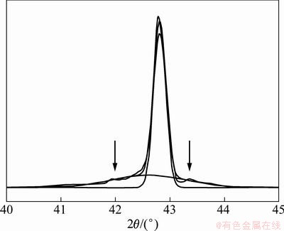
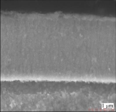
Figure 1 shows the X-ray diffraction spectrum of the Cu-14.3%W thin film prepared on the Fe-substrate. The XRD pattern containing crystalline diffraction peaks superimposed on the top of broad background. This broad background was associated with amorphous phase. The structure of the prepared thin film was composed of crystalline and amorphous phase. In order to detect the distribution of the mixed two-phase, the section morphology of Cu-14.3%W thin film prepared on the Cu-substrate was observed using SEM and the result is shown in Fig. 2. The morphology of the thin film was the same as that of Cu-substrate except the surface morphology of the thin film which was indistinct. To discover the characteristics of the structure, the Cu-14.3%W thin film prepared on the NaCl-substrate was used and the NaCl was removed using alcohol. The film was either ion-milled from the bottom side (near the substrate) for the analysis of the microstructure of the film surface, or ion-milled from the top surface of the film for the analysis of the microstructure of the film bottom. The thickness of the TEM sample was about 100 nm. The non-crystalline maybe occurred during ion-milling process; however, it did not affect the observing results of the original sample because the non-crystalline formed by ion-milling was only several nanometers [16].

Fig. 1 X-ray diffraction spectrum of Cu-14.3%W thin film prepared on Fe-substrate

Fig. 2 Section morphology of Cu-14.3%W thin film prepared on Cu-substrate
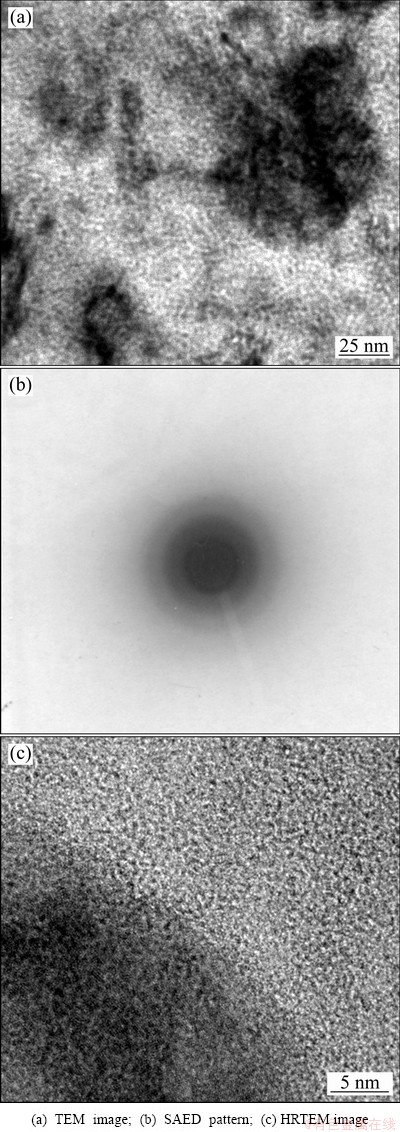
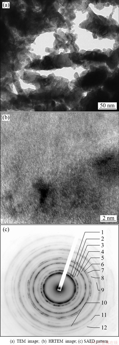
Figure 3 shows the TEM micrograph and the corresponding selected-area electron diffraction (SAED) pattern for Cu-14.3%W film deposited on NaCl- substrate for 100 min. The sample was taken from the surface of the film, which was regarded as the initial stage of sputtering. The SAED result showed only an amorphous diffraction halo, indicating that the surface structure of the deposited film was mainly amorphous. The HRTEM micrograph (Fig. 3(c)) for Cu-14.3%W film confirmed that the structure of the film was a predominantly amorphous matrix. TEM micrograph and SAED pattern from the bottom of Cu-14.3%W film deposited on NaCl-substrate for 100 min are shown in Fig. 4. The SAED result shows a polycrystalline diffraction ring, indicating that the structure of the bottom of deposited film is polycrystalline.

Fig. 3 Surface structures of Cu-W film deposited on NaCl-substrate for 100 min
Figure 5 shows the XRD patterns of the Cu1-xWx alloy films (x=13.7%, 18.1%). The sideband effect appeared on both sides of the (111) peak of Cu (W) solid solution, which was similar to the diffraction pattern caused by spinodal decomposition.

Fig. 4 Bottom structures of Cu-W film deposited on NaCl- substrate for 100 min
4 Discussion
As we know, spinodal decomposition was one of the way for the decomposition of supersaturated solid solution��where poverty- and rich-solute atoms areas form. The sideband effect of X-ray diffraction appeared on both or one sides of the main peak. The sideband peak can also be clearly found out in Fig. 1, referred as arrows. It illustrated that the different compositions of solid solution formed during preparation. The calculated results of the electron diffraction pattern shown in Fig. 4(c) are listed in Table 1, which confirmed that the Cu-14.3%W thin film was composed of Cu(W) solid solutions with different compositions. Diffraction rings were formed by the fine grains in the Cu (W) solid solution. The sidebands in XRD and diffraction rings in SAED illustrated that the analogy spinodal structure formed in the Cu-W thin film during sputtering deposition process. The data of X-ray diffraction of Cu1-xWx alloy films (x=13.7%, 14.3%, 18.1%) are listed in Table 2. The position of main peak located between 42.987�� and 42.631��. Positions of the peaks on the right side of main peak were all higher 43.295�� than that of the (111)Cu of the Cu-PDF (4-836), and these peaks were not formed by Cu(W)solid solution because the atom radius of W was larger than that of Cu. The lattice parameter and interplanar distance of Cu should expand if W dissolved in the Cu-matrix. Therefore, the peaks on the right side of main peaks were formed by pure Cu. The 2�� was higher than that of pure Cu and can be attributed to the compressive stress formed during preparation. The main peak and that of the left side of main peak were formed by Cu (W) solid solution with different contents of W.

Fig. 5 X-ray diffraction spectra of Cu1-xWx film deposited for 100 min
Table 1 Index results of polycrystalline diffraction ring

Table 2 Estimated results of solid solubility of Cu-W alloy films with different W contents

The position change of the diffraction peaks of Cu-W film was caused by solid solubility and the internal stress of thin films. The 2�� of (111)Cu from the dual-target magnetron sputtering deposition film was higher than that in PDF, which can be attributed to the compressive stress formed during preparation.
In general, the lattice parameter of solid solution varied with the concentration of solute atoms and obeys the Vegard law, which can be expressed as follows:
 (1)
(1)
where ax is the lattice parameter of solid solution; aA is the lattice parameter of solute A atom; aB is the lattice parameter of solvent B atom; and x is the concentration of A atoms in the B(A) solid solution.
The lattice parameters of W should adopt the parameter of FCC structure as the W atoms replace the Cu atoms in the Cu (W) solid solution. However, under normal conditions, the crystal structure of Cu was FCC and that of W was BCC, and W with FCC structure did not exist. Different models have been established to calculate the lattice parameters of W with FCC structure. The lattice parameters of W with FCC structure have been calculated using the atomic stacking model��which was similar to calculating the lattice parameters of Mo with FCC structure [17], and the results are listed in Table 3.
Table 3 Lattice parameters of Cu and W with FCC and BCC crystal structure

In order to estimate the solid solubility using the Vegard law, the position change of the diffraction peaks of Cu-W film caused by internal stress should be deduced. The changing angle of the (111) Cu in the X-ray diffraction profile was taken as that caused by the internal stress and the estimated results are listed in Table 2. Based on the calculated FCC-W lattice parameters, the relationship between lattice parameter and concentration of the solute atoms has been established using the Vegard law, the solid solubility was estimated, and the results are listed in Table 2. From Table 2, Cu-W films with the designed W content less than 18.2% formed a mixture of three kinds of solid solution with different components. For Cu-W films with the average W content of 13.7%, the solid solution was composed of Cu(W) solution with 37% of W, Cu(W) solution with 11% W and pure Cu. For Cu-W films with the average W content of 14.3%, it was composed of Cu(W) solution with 38% W, Cu(W) solution with 15% W and pure Cu. For Cu-W films with the average W content of 18.1%, it was composed of Cu(W) solution with 36%W, Cu(W) solution with 19% W and pure Cu.
A negative heat of mixing was generally considered a necessary condition for the formation of amorphous materials in solid-state reactions. However, in some non-equilibrium processes, such as rapid quenching and sputtering, amorphous alloys can be formed regardless of positive or negative values of heat of mixing. In an immiscible system, a thermodynamic driving force can lead to the interfacial mixing of the clusters of the constituent elements, as long as the driving force is greater than the positive heat of mixing of the system. The Gibbs free energy diagram of the Cu-W multilayer system established using Miedema��s model gave a reasonable interpretation; the observed solid-state alloying was driven by the interfacial energy [18].
In dual-target magnetron sputtering deposition process, Cu and W atoms or small clusters broke away from the target and formed clusters during the flight from the target to the substrate. MA [19] described the clustering and amorphizing process in immiscible systems by MD simulation. When these clusters landed on the substrate, the phase transition can be determined by their surface diffusivity. At a low substrate temperature, the atoms or clusters were largely immobilized on the substrate with finite diffusion distances. These clusters can randomly form islands on the substrate, leading to an amorphous state. A general expression used to estimate average diffusion distance of a deposited atom was [20]
 (2)
(2)
where v is the vibrational frequency; a is the individual jump distance; R is the deposition rate, which depends on the sputter condition; Qs is the activation energy for surface diffusion; k is the Boltzmann��s constant; and T is the substrate temperature (K). RIZZO et al [6] derived formulae for estimating the activation energy from the sublimation energy (��Hsub1). Qs is 0.24 ��Hsub1 for FCC metals and Qs is 0.33��Hsub1 for BCC metals, when the temperature is less than 0.75 of the melting temperature of the metal. The values of Qs estimated using these formulae for Cu and W were that:  =~0.78 eV and
  =~2.94 eV. The average diffusion distances of W and Cu atoms were estimated to be 10-16 nm and 1 nm, respectively. In other words, at a low deposition temperature, surface diffusion of W virtually did not take place while the Cu atoms can move a short distance. Therefore, amorphous phases on an atomic or cluster scale formed at low deposition temperatures. Whereas, the surface of the deposited film (Fig. 3) was an amorphous layer embedded with small crystalline phase regions, the microstructure of the bottom of the deposited film was mainly crystalline (Fig. 4). From the micrograph of Cu-W film deposited for 100 min, it can be deduced that the structure of the initial film on the substrate was amorphous and gradually transformed into a metastable solution during the deposition process. The transformation from amorphous to metastable solution was due to the additional energy provided by the continuous magnetic sputtering.
During dual-target magnetron sputtering deposition process, the atoms in the initially amorphous phase can gain extra energy due to the bombardment of the subsequent sputtering particles generated by further magnetic sputtering. The mobility of the atoms in the amorphous phase was improved. Nuclei for crystallization were easier to form, leading to crystallization of the pre-deposited amorphous layer. MIEDEMA et al [21] reported that the heat of solution of Cu in W was +86 kJ/mol (0.89 eV) and the heat of solution of W in Cu was +107 kJ/mol (1.11 eV). During the sputtering process, the kinetic energy of the sputtered particles (clusters or atoms) was about 10 eV [22,23], which is much higher than the heat of solution between Cu and W. The kinetic energy of the sputtering particles is sufficient to overcome the heat of solution and the formation of a solution of the two metals can readily take place. The initially amorphous Cu-W phase in the bottom of the deposited film therefore crystallized, and the initially amorphous Cu-W phase transformed into solid solution with different W contents due to the diffusion of Cu atoms. The average diffusion distances of W- and Cu-atom were estimated to be 10-16 nm and 1 nm, respectively. The W atoms almost fixed and the Cu atoms shortly diffused due to the bombardment of the subsequent sputtering particles generated by further magnetic sputtering. The Cu-crystal with FCC structure was formed owing to its short distance diffusion. Cu atoms moved around W atoms or W atoms cluster into their positions of FCC stacking structure, and formed the substitutional solid solution. Cu atoms and W atoms could not be evenly mixed at the atomic level, therefore, analogy spinodal structure of the solid solution with different W contents deformed. The surface region of the film, however, had not been subjected to sufficient bombardment of the sputtering particles. Therefore, it remained amorphous.
5 Conclusions
1) Immiscible Cu-W alloy thin films were prepared using dual-target magnetron sputtering deposition process. The structure of the prepared thin film is composed of crystalline and amorphous phase. The distribution of the crystalline and amorphous phase shows the layer structure.
2) In the dual-target magnetron sputtering deposition process, the Cu and W atoms or clusters deposited on the substrate first form an amorphous phase, then crystallize by the bombardment of the post- sputtering energetic particles, and form the analogous spinodal structure. The surface region of the film remains amorphous because of no further bombardment.
3) The solid solubility was calculated using the Vegard law. For Cu-W film with W content of 13.7%, it is composed of Cu( W) solution with 11% W, Cu( W) solution with 37% W and pure Cu; for Cu-W film with W content of 14.3%, it is composed of Cu(W) solution with 15% W, Cu(W) solution with 38% W and pure Cu; for Cu-W film with the W content of 18.1%, it is composed of Cu(W) solution with 19% W, Cu(W) solution with 36% W and pure Cu.
References
[1] RYU S S, KIM G S, KIM J C, OH S T, KIM Y D. The influence of annealing temperature on the microstructural development of W-Cu composite powder prepared by high-energy ball milling [J]. Journal of Alloys and Compounds, 2006, 424(1-2): 209-212.
[2] RAPE A, CHANTHAPAN S, SINGH J, KULKARNI A. Engineered chemistry of Cu-W composites sintered by field-assisted sintering technology for heat sink applications [J]. Journal of Materials Science, 2011, 46(1): 94-100.
[3] VENUGOPAL T, PRASAD RAO K, MURTY B S. Synthesis of Cu-W nanocomposite by high-energy ball milling [J]. Journal of Nanoscience and Nanotechnology, 2007, 7(7): 2376-2381.
[4] TAI K P, AVERBACK R S, BELLON P, ASHKENAZY Y, STUMPHY B. Temperature dependence of irradiation-induced creep in dilute nanostructured Cu-W alloys [J]. Journal of Nuclear Materials, 2012, 422(1-3): 8-13.
[5] RADI��C N, GRZETA B, GRACIN D, CAR T. Preparation and structure of Cu-W thin films [J]. Thin Solid Films, 1993, 228(1-3): 225-228.
[6] RIZZO H F, MASSALSKI T B, NASTASI M. Metastable crystalline and amorphous structures formed in the Cu-W system by vapor deposition [J]. Metallurgical and Materials Transactions A, 1993, 24(5):1027-1037.
[7] RADI��C N, STUBICAR M. Microhardness properties of Cu-W amorphous thin films [J]. Journal of Materials Science, 1998, 33(13): 3401-3405.
[8] ZONG R L, WEN S P, ZENG F, GAO Y, PAN F. Nanoindentation studies of Cu�CW alloy films prepared by magnetron sputtering [J]. Journal of Alloys and Compounds, 2008, 464(1-2): 544-549.
[9] DIRKS A G, van den BROEK J J. Metastable solid solutions in vapor deposited Cu-Cr, Cu-Mo, and Cu-W thin films [J]. Journal of Vaccum Science and Technology A: Vacuum, Surface, and Films, 1985, 3(6): 2618-2622.
[10] ZHANG R F, LI Z G, LIU B X. Metastable phase formed in immiscible Cu-W multilayers by ion mixing [J]. Japanese Journal of Applied Physics, 2003, 42(1): 7009-7012.
[11] GAO Y, YANG T F, XUE J M, YAN S, ZHOU S Q, WANG Y G, KWOK D T K,
[12] BUKHANOVSKY V V, GRECHANYUK N I, MINAKOVA R V, MAMUZICH I, KHARCHENKO V V, RUDNITSKY N P. Production technology, structure and properties of Cu-W layered composite condensed materials for electrical contacts [J]. International Journal of Refractory Metals & Hard Materials, 2011, 29(5): 573-581.
[13] BUKHANOVSKY V V, MINAKOVA R V, GRECHANYUK I N, MAMUZIAE I, RUDNITSKY N P . Effect of composition and heat treatment on the structure and properties of condensed composites of the Cu-W system [J]. Metal Science and Heat Treatment, 2011, 53: 14-23.
[14]
[15] WANG Y, XU K W. Cu-W Thin film characterized by surface fractal and resistivity [J]. Acta Physical Sinica, 2004, 53(3): 900-904.
[16] MCCAFFREY J P, PHANEUF M W, MADSEN L D. Surface damage formation during ion-beam thinning of samples for transmission electron microscopy [J]. Ultramicroscopy, 2001, 87(3): 97-104.
[17] XI S Q, ZUO K S, LI X G, RAN G, ZHOU J G. Study on the solid solubility extension of Mo in Cu by mechanical alloying Cu with amorphous Cr (Mo) [J]. Acta Materialia, 2008, 56(20): 6050-6060.
[18] CHEN Y G, LIU B X. Interface-driven solid-state alloying in an immiscible Cu-W system [J]. Journal of Physics D: Applied Physics, 1997, 30(12): 1729-1730.
[19] MA E. Alloys created between immiscible elements [J]. Progress in Materials Science, 2005, 50(4): 413-509.
[20] SAUNDERS N, MIODOWNIK A P. Phase formation in co-deposited metallic alloy thin films [J]. Journal of Materials Science, 1987, 22(2): 629-637.
[21] MIEDEMA A R, de  P F, de BOER F R. Cohesion in alloys-Fundamentals of a semi-empirical model [J]. Physica B, 1980, 100(1): 1-28.
[22] SMITH D L. Thin films deposition [M]. New York: McGraw-Hill Inc, 1995: 132.
[23] MUSIL J,  J. Magnetron sputtering of alloy and alloy-based films [J]. Thin Solid Films, 1999, 343-344: 47-50.
����ƽ1, 2��������1, 3���� ��2����ҿ�2���� ��1���� ��1
1. ���ϴ�ѧ ���Ͽ�ѧ�빤��ѧԺ����ɳ 410083��
2. ���ϴ�ѧ ���Ͽ�ѧ�빤��ѧԺ����ɳ 410082��
3. ��������ɫ�������Ͽ�ѧ�빤���ص�ʵ���ң���ɳ 410083
ժ Ҫ������˫�дſؽ������Cu-W�Ͻ�Ĥ��ͨ��XRD��TEM��HRTEM�ȷ�������������Ĥ��֯�ṹ�����ݱ���ɡ��ڳ������ڣ�Cu-W��Ĥ�ʷǾ�̬�����ų������̵Ľ��У��ڽ������ӵĺ�����ѳ�����Ĥ�������γ�������ṹ���Ӷ��ڳ�����ɵ���Cu-W��Ĥ�г��ֱ���Ϊ�Ǿ�̬���ײ�Ϊ��̬�IJ�״�ṹ������Vegard�����������ṹ�Ĺ��ܶȽ��м��㣬Cu-13.7%W��Ĥ���ɹ��ܶȷֱ�Ϊ11%W��37%W��Cu(W)�����弰��Cu����ɣ�Cu-14.3%W��Ĥ���ɹ��ܶȷֱ�Ϊ15%W��38%W��Cu(W)�����弰��Cu����ɣ�Cu-18%W��Ĥ���ɹ��ܶȷֱ�Ϊ19%W��36%W��Cu(W)�����弰��Cu����ɡ�
�ؼ��ʣ�Cu-W��Ĥ������������Ǿ��ࣻ��״�ṹ�����ܶȣ�Vegard����
(Edited by LI Xiang-qun)
Corresponding author: LI Zhou; Tel: +86-731-88830264; Fax: +86-731-88876692; E-mail: lizhou6931@163.com
DOI: 10.1016/S1003-6326(11)61520-3

