Trans. Nonferrous Met. Soc. China 22(2012) s127-s132
Microstructure and electrical properties of sol-gel derived Ni-doped CaCu3Ti4O12 ceramics
ZHANG Cheng-hua1, 2, 3, 4, 5, ZHANG Ke1, 5, XU Hong-xing1, SONG Qi1, 5, YANG Yong-tao1, 6, YU Ren-hong1, 6, XU Dong1, 2, 3, 4, 5, CHENG Xiao-nong1, 5
1. School of Material Science and Engineering, Jiangsu University, Zhenjiang 212013, China;
2. Key Laboratory of Semiconductor Materials Science, Institute of Semiconductors, Chinese Academy of Sciences, Beijing 100083, China;
3. State Key Laboratory of Electrical Insulation and Power Equipment, Xi’an Jiaotong University, Xi’an 710049, China;
4. State key Laboratory of Electronic Thin Films and Integrated Devices, University of Electronic Science and Technology of China, Chengdu 610054, China;
5. Changzhou Engineering Research Institute of Jiangsu University, Changzhou 213000, China;
6. Changzhou Ming Errui Ceramics Co., Ltd., Changzhou 213102, China
Received 9 July 2012; accepted 20 August 2012
Abstract: Dielectric properties and varistor performance of sol-gel prepared Ni-doped calcium copper titanate ceramics (CaCu3NixTi4O12+x, x=0, 0.1, 0.2, 0.3) were investigated. SEM and XRD were used in the microstructural studies of the specimens and the electrical properties were investigated for varistors. XRD patterns show that the CCTO ceramics were single phase with no Cu-rich phase. SEM results indicated that the samples had smaller grain sizes than those synthesized by traditional solid-state reaction methods. The experimental results show that the highest dielectric constant and lower dielectric loss occur when x=0.2. When x=0.3, the lowest leakage current is obtained and the maximum value reaches 0.295; meanwhile, the lowest threshold voltage and nonlinear coefficient are found, the minimum values of them are 1326 V/mm and 3.1, respectively.
Key words: CaCu3Ti4O12; sol-gel; capacitors; memory devices; electrical properties; microstructure; phase transition
1 Introduction
The perovskite titanate CaCu3Ti4O12 (CCTO) has generated ever-increasing attention because of its high dielectric constant (~104) and weak temperature dependence between 100 K and 400 K without any structural phase transition [1-5]. Such unusual physical features make it a promising material for microelectronics including capacitors and memory devices. It was reported by HOMES et al [6] that the relative dielectric constant εr of single crystalline CCTO is close to 105 at frequency below 20 kHz when the temperature is 250 K. Giant dielectric constant has been ascribed to barrier layer formation at grain boundaries or due to formation of twin boundaries [3-5, 7-9], whereas, some researchers attributed it to local dipole moments associated with off center displacement of Ti ions [10]. So far there is still some dispute on the mechanism of the giant dielectric constant.
Besides the giant dielectric properties, CCTO has also been provided with the non-ohmic response. CHUNG et al [11] discovered that the bulk CCTO ceramics showed nonlinear current-voltage characteristics and the nonlinear coefficient was about 900, which was much greater than that of conventional ZnO varistor. Atomic force microscopy revealed the presence of an intrinsic electrostatic potential barrier at the grain boundaries that is considered to be responsible for the varistor properties [11]. This outstanding electrical performance is quite unusual since CCTO exhibits a body centered cubic perovskite structure with slightly tilted [TiO6] octahedra facing each other, in other words, the compound is not ferroelectric. Compared to the traditional methods,the sol-gel method has many advantages, such as simple process, preparation process, no pollution, low energy consumption, may obtain higher degree (molecular scale) uniformity.
Doping is the common means in materials research. The electrical properties can be greatly affected by appropriate doping and elements substitution [12,13]. According to the reports [14], NiO is also high dielectric material, and the reports about Ni-doped CCTO ceramics have been seen. So in this work, sol-gel process is used to fabricate the Ni-doped CCTO ceramics. And the influences of the Ni amount on the microstructure and dielectric properties of CCTO have been investigated.
2 Experimental procedure
The sol-gel method was used to prepare the powders following the composition of CaCu3NixTi4O12+x, for x=0, 0.1, 0.2, 0.3 (sample labeled ZB0, ZB1, ZB2, ZB3 respectively). The reagent-grade raw materials were calcium acetate [Ca(CH3COO)2・H2O], copper nitrate [Cu(NO3)2・3H2O], NiNO2 and tetrabutyl titanate [Ti(OC4H9)4]. Firstly, an appropriate amount of Ca(CH3COO)2・H2O, Cu(NO3)2・3H2O, NiNO2 and Ti(OC4H9)4 in the stoichiometric ratio were dissolved in ethanol separately with some glacial acetic acid. Secondly, proper amount of deionized water and little nitric acid were added when the sol was stirred. After continual stirring for about 20 min, a cyan precursor sol was obtained. And then, after aging for 24 h at 50 °C, the gel precursor was dried at 150 °C in a drier. Finally, the dried gel was decomposed at 900 °C for 8 h to obtain the CCNTO powders. Then the obtained powders were ground with polyvinyl alcohol solution (PVA) and compacted into pellets that were 12 mm in diameter and about 1.5 mm in thickness. The samples were sintered in air at 1050 °C for 16 h. For the characterization of DC current-voltage, the silver paste was coated on both faces of samples and the silver electrodes were formed by heating at 600 °C for 10 min. The electrodes were 5 mm in diameter.
The voltage-current (V-I) characteristics were measured using a V-I source/measure unit (CJP CJ1001). The nominal varistor voltages (VN) at 0.1 and 1.0 mA were measured [4, 15-21] and the threshold voltage VT (V/mm). VT= /d, where, d is the thickness of the sample (mm); is the nominal varistor voltage at 1 mA. The leakage current (IL) was measured at 0.75VN (1 mA). The measurement accuracy for voltage was ±0.5% and for electric current ±2%. In addition, the nonlinear coefficient α values (α=1/lg(V1/V2), V1 and V2 are the voltages at 1.0 mA and 0.1 mA, respectively) were determined with relative error of ±5% [16-18, 21-27]. The crystalline phases were identified by an X-ray diffraction (XRD, Rigaku D/max 2500, Japan) using a Cu Kα radiation. The dielectric characteristics, such as the apparent dielectric constant (ε) and dissipation factor (tan δ) at different frequencies were measured by an HP4294A impedance analyzer (Agilent).
3 Results and discussion
Figure 1 shows XRD patterns of various Ni-doped CCTO varistors. These patterns are essentially similar to that of undoped CCTO ceramic. The XRD data were indexed on the basis of a cubic unit cell similar to CCTO. Moreover, no secondary phases containing Ni are detected up to x=0.30, because XRD is not sensitive to concentrations under 0.5% (mass fraction) [12-14, 20], which confirm the good crystallinity of these samples. The XRD peaks intensify with the increasing of Ni doping concentration, which suggest that dopant promotes the formation of the main crystalline phase of CCTO ceramic.
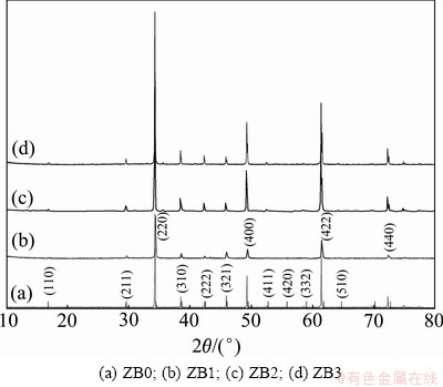
Fig. 1 XRD patterns of various Ni-doped CCTO varistors sintered at 1050 °C in air for 16 h
The SEM images of the samples are shown in Fig. 2. It is clear that the samples have porous structures. There are no secondary phases observed in the undoped CaCu3Ti4O12, such as a Cu-rich precipitate composition, as is often reported in the Refs. [28,29], and these are in accordance with the XRD analysis. The same average grain sizes were approximately 2 μm. In comparison to traditional solid-state reaction methods [24,28,29], smaller grain sizes can be obtained from samples which are synthesized by the sol-gel method. In previous work [3], the grain size decreased obviously with increase of amount of dopant. However, such an obvious change trend of the grain size can’t be acquired in this work. Even so, it could not be ignored that the Ni doping is helpful to increase the uniformity of CCTO samples. The grain size of sample ZB3 is more homogeneous than that of other samples. Moreover, some small white dots can be observed in the sample ZB3 (x=0.3) image, which are not observed in the samples ZB1 and ZB2. We believe that the small white dots are Ni doping.
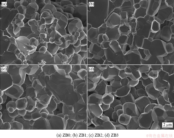
Fig. 2 SEM images of fracture of samples
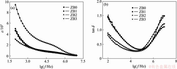
Fig. 3 Frequency dependence of dielectric constant (εr) and dielectric loss (tan δ) at room temperature
Figure 3 illustrates the dielectric constant and dielectric loss with frequency from 100 Hz to 30 MHz at room temperature. The εr of the pure CCTO is about 1700 at 1 kHz which is close to that reported by some reports [27-29]. But it is much less than that reported in some other papers [30]. We consider the powders decomposed from the dried gel are smaller than that obtained from solid-state reaction. More cavities will be produced in the samples without the PVA addition. Thus, smaller grain will be obtained for that the pores impede the growth of the grain. According to the previous work [3], the larger grain size will help to obtain a higher dielectric constant. The reason of the relatively small dielectric constant can be easily understood. The dielectric constant decreases as the frequency increases. In addition, sample ZB2 has the highest dielectric constant among these samples, while other samples have the similar dielectric constant. As Ni content increases, the dielectric loss tends to decrease in the low frequency region and increase in the high frequency region. Lower dielectric loss can be observed in samples ZB2 and ZB3. Obviously, the highest dielectric constant and lower dielectric loss occur when x=0.2, that is to say, sample ZB2 has better dielectric property.
XPS analysis was carried out to investigate the valence states of ions in CCTO ceramics [31]. Figure 4 shows the XPS spectra of O1s, Ca 2p, Ti 2p and Cu 2p. The shift of core-level spectra due to charging effect was calibrated using the contaminated C 1s peak located at 285 eV. As seen from Fig. 4(a), O1s peak can be spitted into two peaks, one is due to Cu―O bonds and the other is due to Ca―O bonds [32]. It is revealed that presence of calcium in +2 oxidation state is clear from the shape, the symmetry of the peak and the bonding energy of Ca 2p in Fig. 4(b) [33]. Fig. 4(c) shows the XPS pattern of Ti 2p. Titanium is in the +4 state, which is evident from the shape, the symmetry of the peak and the bonding energy of Ti 2p. Copper exists mostly in the +2 oxidation state observed from Fig. 4(d), and sample ZB2 illustrates that some copper exists in +1 state. The presence of most copper in +2 oxidation states is evidenced from the bonding energy of the 2p3/2 level and also the peak of O 1s in Fig. 4(a).
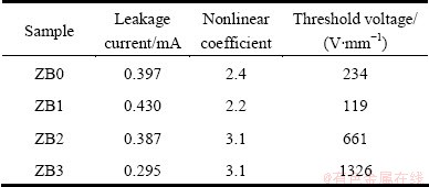
As seen from Table 1, Ni doping shows remarkable influences on the nonlinear current-voltage properties of CCTO samples. As the Ni doping increases, the leakage current increases firstly and then decreases, while nonlinear coefficient and threshold voltage present an opposite tendency. When x=0.1, the highest leakage current is obtained and the maximum value reaches 0.43; meanwhile, the lowest threshold voltage and nonlinear coefficient are found, the minimum values of them are 119 V/mm and 2.2, respectively. Sample ZB3 displays good synthetical properties which has the lowest leakage current, and shows better nonlinear V-I characteristics than other samples. It can be accounted for that the Ni doping increases CCTO grain boundary barrier, leading to nonlinear coefficient and threshold voltage rising up and leakage current reducing. The electrical characteristics of the varistor ceramics are at their best when x= 0.3.
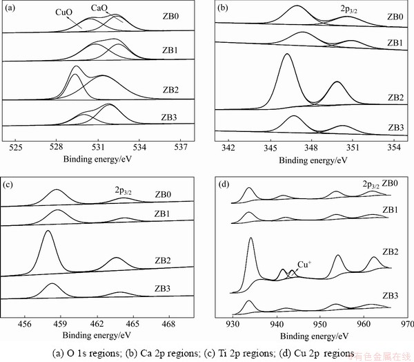
Fig. 4 X-ray photoelectron spectroscopy spectra of CCTO ceramics
Table 1 Electrical properties of Ni-doped CCTO ceramics
4 Conclusions
1) The CaCu3NixTi4O12+x (x=0, 0.1, 0.2, 0.3) ceramics can be prepared by the sol-gel method. XRD patterns show that there is only one phase (CCTO phase) in different samples, along with dopant promotes the formation of the main crystalline phase of CCTO ceramic. SEM results reveal that the same average grain sizes of samples were approximately 2 μm, which are much smaller than that synthesized by the traditional solid-state reaction methods. And Ni doping is helpful to increase the uniformity of CCTO samples.
2) The electrical measurements demonstrate that the CaCu3Ni0.2Ti4O12.2 (the sample with x=0.2) has the best dielectric property due to its highest dielectric constant and lower dielectric loss. The CaCu3Ni0.3Ti4O12.3 (the sample with x=0.3) displays good varistor properties, which can be accounted for that the Ni doping increases CCTO grain boundary barrier, leading to nonlinear coefficient and threshold voltage rising up and leakage current reducing.
References
[1] SUBRAMANIAN M A, LI D, DUAN N, REISNER B A, SLEIGHT A W. High dielectric constant in ACu3Ti4O12 and ACu3Ti3FeO12 phases[J]. Journal of Solid State Chemistry, 2000, 151(2): 323-325.
[2] RAMIREZ A P, SUBRAMANIAN M A, GARDEL M, BLUMBERG G, LI D, VOGT T, SHAPIRO S M. Giant dielectric constant response in a copper-titanate [J]. Solid State Communications, 2000, 115(5): 217-220.
[3] XU D, ZHANG C, CHENG X N, FAN Y E, YANG T, YUAN H M. Dielectric properties of Zn-doped CCTO ceramics by sol-gel method[J]. Advanced Materials Research, 2011, 197-198: 302-305.
[4] XU D, ZHANG C, LIN Y H, JIAO L, YUAN H M, ZHAO G P, CHENG X N. Influence of zinc on electrical and microstructural properties of CaCu3Ti4O12 ceramics prepared by sol-gel process [J]. Journal of Alloys and Compounds, 2012, 522: 157-161.
[5] XU D, WANG B, LIN Y H, JIAO L, YUAN H M, ZHAO G P, CHENG X N. Influence of Lu2O3 on electrical and microstructural properties of CaCu3Ti4O12 ceramics [J]. Physica B: Condensed Matter, 2012, 407(13): 2385-2389.
[6] HOMES C C, VOGT T, SHAPIRO S M, WAKIMOTO S, RAMIREZ A P. Optical response of high-dielectric-constant perovskite-related oxide [J]. Science, 2001, 293(5530): 673-676.
[7] LUNKENHEIMER P, FICHTL R, EBBINGHAUS S G, LOIDL A. Nonintrinsic origin of the colossal dielectric constants in CaCu3Ti4O12 [J]. Physical Review B, 2004, 70(17210217).
[8] SINCLAIR D C, ADAMS T B, MORRISON F D, WEST A R. CaCu3Ti4O12: One-step internal barrier layer capacitor [J]. Applied Physics Letters, 2002, 80(12): 2153-2155.
[9] LIN Y H, CAI J N, LI M, NAN C W, HE J L. High dielectric and nonlinear electrical behaviors in TiO2-rich CaCu3Ti4O12 ceramics [J]. Applied Physics Letters, 2006, 88(17290217).
[10] KE S, HUANG H, FAN H. Relaxor behavior in CaCu3Ti4O12 ceramics [J]. Applied Physics Letters, 2006, 89 (182904).
[11] CHUNG S Y, KIM I D, KANG S. Strong nonlinear current-voltage behaviour in perovskite-derivative calcium copper titanate [J]. Nature Materials, 2004, 3(11): 774-778.
[12] LIU X Q, WU S Y, CHEN X M. Enhanced giant dielectric response in Al-substituted La1.75Sr0.25NiO4 ceramics [J]. Journal of Alloys and Compounds, 2010, 507(1): 230-235.
[13] LIN Y H, WANG J F, JIANG L, CHEN Y, NAN C W. High permittivity Li and Al doped NiO ceramics [J]. Applied Physics Letters, 2004, 85(23): 5664-5666.
[14] LIN Y H, LI M, NAN C W, LI J F, WU J B, HE J L. Grain and grain boundary effects in high-permittivity dielectric NiO-based ceramics [J]. Applied Physics Letters, 2006, 89(0329073).
[15] WU Z H, FANG J H, XU D, ZHONG Q D, SHI L Y. Effect of SiO2 addition on the microstructure and electrical properties of ZnO-based varistors [J]. International Journal of Minerals, Metallurgy and Materials, 2010, 17(1): 86-91.
[16] XU D, CHENG X N, WANG M S, SHI L Y. Microstructure and electrical properties of La2O3-doped ZnO-Bi2O3-based varistor ceramics [J]. Advanced Materials Research, 2009, 79-82: 2007-2010.
[17] XU D, SHI L Y, WU Z H, ZHONG Q D, WU X X. Microstructure and electrical properties of ZnO-Bi2O3-based varistor ceramics by different sintering processes[J]. Journal of the European Ceramic Society, 2009, 29(9): 1789-1794.
[18] XU D, SHI L Y, WU X X, ZHONG Q D. Microstructure and Electrical properties of Y2O3-doped ZnO-Bi2O3-based varistor ceramics[J]. High Voltage Engineering, 2009, 35(9): 2366-2370.
[19] XU D, CHENG X N, ZHAO G P, YANG J, SHI L Y. Microstructure and electrical properties of Sc2O3-doped ZnO-Bi2O3-based varistor ceramics [J]. Ceramics International, 2011, 37(3): 701-706.
[20] XU D, CHENG X N, YUAN H M, YANG J, LIN Y H. Microstructure and electrical properties of Y(NO3)3・6H2O-doped ZnO-Bi2O3-based varistor ceramics [J]. Journal of Alloys and Compounds, 2011, 509(38): 9312-9317.
[21] XU D, SHI X F, CHENG X N, YANG J, FAN Y E, YUAN H M, SHI L Y. Microstructure and electrical properties of Lu2O3-doped ZnO-Bi2O3-based varistor ceramics [J]. Transactions of Nonferrous Metals Society of China, 2010, 20(12): 2303-2308.
[22] BERNIK S, DANEU N. Characteristics of ZnO-based varistor ceramics doped with Al2O3 [J]. Journal of the European Ceramic Society, 2007, 27(10): 3161-3170.
[23] BERNIK S, MACEK S, BUI A. The characteristics of ZnO-Bi2O3-based varistor ceramics doped with Y2O3 and varying amounts of Sb2O3 [J]. Journal of the European Ceramic Society, 2004, 24(6): 1195-1198.
[24] LEACH C, LING Z, FREER R. The effect of sintering temperature variations on the development of electrically active interfaces in zinc oxide based varistors [J]. Journal of the European Ceramic Society, 2000, 20(16): 2759-2765.
[25] PEITEADO M, FERNANDEZ J F, CABALLERO A C. Varistors based in the ZnO-Bi2O3 system: Microstructure control and properties [J]. Journal of the European Ceramic Society, 2007, 27(13-15): 3867-3872.
[26] XU D, CHENG X N, YAN X H, XU H X, SHI L Y. Sintering process as relevant parameter for Bi2O3 vaporization from ZnO-Bi2O3-based varistor ceramics [J]. Transactions of Nonferrous Metals Society of China, 2009, 19(6): 1526-1532.
[27] CHANG L, LEE D, HO C, CHIOU B. Thickness-dependent microstructures and electrical properties of CaCu3Ti4O12 films derived from sol-gel process [J]. Thin Solid Films, 2007, 516(2-4): 454-459.
[28] CHANG L, YANG C, KAO H. Influence of carrier injection on resistive switching of CaCu3Ti4O12 thin films with Ni electrode [J]. Thin Solid Films, 2011, 519(15): 5095-5098.
[29] JHA P, ARORA P, GANGULI A K. Polymeric citrate precursor route to the synthesis of the high dielectric constant oxide, CaCu3Ti4O12 [J]. Materials Letters, 2003, 57(16-17): 2443-2446.
[30] LI T, CHEN Z P, CHANG F G, HAO J H, ZHANG J C. The effect of Eu2O3 doping on CaCu3Ti4O12 varistor properties [J]. Journal of Alloys and Compounds, 2009, 484(1-2): 718-722.
[31] NI L, CHEN X M. Enhancement of giant dielectric response in CaCu3Ti4O12 ceramics by Zn substitution [J]. Journal of the American Ceramic Society, 2010, 93(1): 184-189.
[32] MAI Y J, TU J P, XIA X H, GU C D, WANG X L. Co-doped NiO nanoflake arrays toward superior anode materials for lithium ion batteries [J]. Journal of Power Sources, 2011, 196(15): 6388-6393.
[33] RAI A K, MANDAL K D, KUMAR D, PARKASH O. Characterization of nickel doped CCTO: CaCu2.9Ni0.1Ti4O12 and CaCu3Ti3.9Ni0.1O12 synthesized by semi-wet route [J]. Journal of Alloys and Compounds, 2010, 491(1-2): 507-512.
溶胶-凝胶法制备Ni掺杂CaCu3Ti4O12陶瓷的显微组织及电性能
张成华1, 2, 3, 4, 5, 张 柯1, 5, 徐红星1, 宋 琪1, 5, 杨永涛1, 6,于仁红1, 6,徐 东1, 2, 3, 4, 5, 程晓农1, 5
1. 江苏大学 材料科学与工程学院,镇江 212013;
2. 中国科学院半导体研究所 半导体材料科学重点实验室,北京 100083;
3. 西安交通大学 电力设备电气绝缘国家重点实验室,西安 710049;
4. 电子科技大学 电子薄膜与集成器件国家重点实验室,成都 610054;
5. 常州江苏大学工程技术研究院, 常州 213000;
6. 常州明尔瑞陶瓷有限公司,常州 213102
摘 要:采用溶胶凝胶法制备掺杂不同含量NiO(CaCu3NixTi4O12+x,x=0, 0.1, 0.2, 0.3)的CCTO陶瓷,通过扫描电镜和X射线衍射对其显微组织和相成分进行了分析,并研究了NiO掺杂对CCTO介电和压敏性能的影响。研究结果表明:Ni对CCTO陶瓷的相位成分没有影响,与用传统固相法制得的样品相比,用溶胶-凝胶法制成的样品具有更小的晶粒尺寸。从介电测量结果来看,当x=0.2时,样品具有最高的介电常数和最低的介电损耗。当x=0.3时,得到最低的漏电流,最小值为0.295,同时,具有最高的阀值电压与非线性系数,最大值分别为1326 V/mm和3.1。
关键词:钛酸铜钙;溶胶-凝胶法;电容器;记忆装置;电性能;显微组织;相变
(Edited by ZHAO Jun)
Foundation item: Projects (BK2011243, BK2012156) supported by the Natural Science Foundation of Jiangsu Province; Project (EIPE11204) supported by the State Key Laboratory of Electrical Insulation and Power Equipment; Project (KF201104) supported by the State Key Laboratory of New Ceramic and Fine Processing; Project (KFJJ201105) supported by the Opening Project of State key Laboratory of Electronic Thin Films and Integrated Devices; Project (10KJD430002) supported by the Universities Natural Science Research Project of Jiangsu Province; Project (CJ20125001) supported by the Application Program for Basic Research of Changzhou; Project (11JDG084) supported by the Research Foundation of Jiangsu University
Corresponding author: XU Dong; Tel: +86-511-88797633; E-mail: frank@ujs.edu.cn

