���±�ţ�1004-0609(2007)09-1470-05
CuxAlO2 (0.92��x��1.0)�մɵ���������
���������š���������ΰ�����������ϡ���
(������ҵ��ѧ ���Ͽ�ѧ�빤��ѧԺ, ���� 100022)
ժ Ҫ��ʹ�ø��¹����սᷨ�Ʊ���ͬ��ѧ�����ȵ�CuAlO2�մɣ��о�CuxAlO2(0.92��x��1.0)��Cu��AlĦ���ȵ���Ա仯����ṹ�͵������ܵ�Ӱ�졣���������CuxAlO2(0.92��x��1.0)�մ�Ƭ�Ľṹ���ܶ�����xֵ��������Ʒ�Ľᾧ����ã��ܶ�Ҳ��������xΪ0.98ʱ���õ��ܶ����(5.02 g/cm3)�ҽᾧ���õĴ���CuAlO2����Ʒ�Ĺ�ѧ��϶��ԼΪ3.44 eV������xֵ�����ӣ����µ絼��������Ȼ���С����xΪ0.98ʱ�õ����絼��Ϊ8.03��10?3 S/cm���絼�����¶ȵ����߶�����������������100~300 K֮��ܺõط���Arrhenius��ϵ��xΪ0.98ʱ��������ͣ���Ϊ0.085 eV�������о��ijɷַ�Χ�ڣ�CuAlO2�մɵĵ���������Ҫȡ�����մ�Ƭ�����ܶȡ�
�ؼ��ʣ�CuAlO2�մɣ�ͭ����ṹ�����ܶȣ��絼�ʣ��ȼ�����
��ͼ����ţ�TN 304���� ���ױ�ʶ�룺A
Electrical transport properties of CuxAlO2 ceramics
DONG Guo-bo, ZHANG Ming, LAN Wei, ZHU Man-kang, YAN Hui
(College of Materials Science and Engineering, Beijing University of Technology, Beijing 100022, China)
Abstract: The nonstoichiometric CuxAlO2 ceramics were successfully prepared by solid state sintering at high temperature. The effects of the x value on the band gap and electrical conductivity were investigated. The results show that the structure and density of CuxAlO2 ceramic plates show a notable improvement with the increasing content of Cu. The maximum value of density is 5.02 g/cm3 for CuxAlO2 ceramic with x=0.98 and the XRD pattern indicates that it is a pure CuAlO2 phase. The optical band gap of CuxAlO2 ceramics is about 3.44 eV. The conductivity at room temperature increases first and then reduces with the increasing content of Cu. The maximum conductivity is about 8.03��10?3 S/cm with x=0.98. The temperature dependence of electrical conductivity agrees well with the Arrhenius relationship, indicating that the electrical conducting is ascribed to thermal activation in the range of 100?300 K. The minimal value of the activation energy is estimated 0.085 eV. The electrical conductivity of CuxAlO2 ceramics mainly depends on the density of the samples in the investigating range.
Key words: CuAlO2 ceramics; delafossite; density; electrical conductivity; activation energy
1997�꣬Kawazoe��[1]������p��CuAlO2��Ĥ����������˼۴���ѧ��������(CMVB)���Ӷ�Ϊp��������������(TCO)������һ���µ��о�;����ҲΪ����ʵ�ֵ�������������[2]�춨�����ۺ�ʵ�������p�͵����������Ĥ���Ʊ������������Լ���Ϊ��Ѩע������缫������л�����������Ч�ʵ��Ƿdz���Ҫ��[3?5]������ĿǰΪֹp��CuAlO2��Ĥ�ĵ絼����Ȼ�ܵͣ��뷢չ�Ƚϳ����n��TCO���С3~4������������Ҳͬʱ��p��TCO���о��ṩ�˽ϴ�Ŀռ䡣���ڶ��Ʊ�p��CuAlO2��Ĥ�ķ� ��[6?10]�У��ſؽ��䷨������жвĵ������ԡ���Ĥ��ȵĿɿ��ԡ������Ʊ��������Ա�Ĥ�Լ����㾭��[11]���ص��Ϊ�����õķ��������������İв��ǽ��䷨��Ĥ���������Ļ������⡣��CuxAlO2�մ��У��մɵĽṹ�������Զ��ܹ�Ӱ���䵼��������Ŀǰ�ⷽ����о����١�
��������ͨ���ı�CuxAlO2�մ��е�xֵ (0.92��x��1.0)�о��մ���ϵ�ṹ�������Եı仯���Լ����մɵ��������ܷ����Ӱ�졣
1 ʵ��
�Է�����Cu2O��Al(OH)3��ĩΪԭ�ϣ����ù����սᷨ�Ʊ�CuxAlO2�մ�[12?13]�����Ƚ�����ԭ�ϰ���ͬ��ѧ�����Ȼ����ĥ24 h����ɺ�����Al2O3�մɹ��У��ڹ�̼������¯�����ա�����500 ���±���1 h��ʹAl(OH)3��ȫ�ֽ⣬Ȼ��������1 100 �棬�ս�10 h�����ս�õķ�ĩ����ĥ24 h����ɺ��������[14]������ѹ����ѹ����(��ʵ����õ�ѹǿΪ500 MPa)������PVA����1 100 �������ս�4 h��ʵ����֤ʵ������ѵ��ս���������ս���ԲƬ��Ʒ���澫ĥ������������Ϳˢ���缫���е����ܲ��ԡ�
CuxAlO2�մɵĽṹʹ��BRUKER?AXS D8 Advance X����������(Cu K������=0.154 056 nm��40 kV�� 40 mA)���в��ԡ����þ���Ϊ0.02 mm���α꿨�߲����մ���Ʒ�ĺ�Ⱥ�ֱ������METTLER TOLEDO �ܶȲ����Dz�����Ʒ���ܶȡ���������ʹ��SHIMADZU��˾��UV?3101PC�Dz���������Agilent E5273��Lakeshore 340�����Զ����Ʊ��µ�ѹ��������ϵͳ�������ºͱ��µ����ʡ�
2 ���������
2.1 �մɵ�XRD����
��ʹ��Cu2O��Al(OH)3��ĩ������������CuAlO2�Ĺ����У������¶ȵ����߷����Ļ�ѧ��Ӧ ��[12?13]
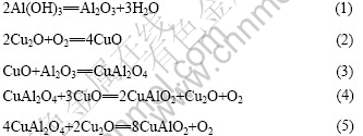
�����Ϸ�Ӧ����ʽ���Կ������ڸ���ϵ�У���Ӧ�ڽϵ��¶�ʱ�����ɼ⾧ʯ�͵�CuAl2O4���ڽϸ��¶������ȶ���ͭ����ṹ��CuAlO2����Щ����ڱ任�ս�ʱ����ս��¶ȵ�ʵ���еõ�����֤��ͼ1��ʾΪ�Ʊ���CuxAlO2�մɵ�XRD�ף���ͼ��ȫ����CuAlO2 PDF 35?1401������ס����Կ�����ֻ����x=1.0ʱ������������CuO��������Ϊ���������Cu������������ӣ��ڿ������������ŷ�Ӧ�Ľ������ɵ�Cu2O���������¡�����������ս���մ���Ʒ���õ��˽ϴ���ͭ����ṹ��CuxAlO2��
ͼ1 CuxAlO2�մɵ�XRD��
Fig.1 XRD patterns of CuxAlO2 ceramics
2.2 �մɵ������Է���
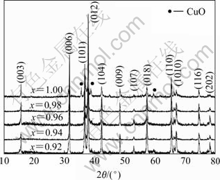
ͼ2��ʾΪCuxAlO2�մ�ϵ�е��ܶ���xֵ�ı仯���ɣ��մɵ�����ܶȲ���Archimedes��ˮ�����������㹫ʽ���£�

ͼ2 CuxAlO2�մɵ��ܶ�
Fig.2 Density of CuxAlO2 ceramics
��ͼ2�ɼ����ڸ���ϵ(0.92��x��1.0)������xֵ�������մɵ��ܶ��������ӡ���x=0.98ʱ���մ��ܶȴﵽ���ֵ5.02 g/cm3��������Ϊxֵ��Сʱ���մ��ڲ���Ϊ�������϶࣬��Ȼ�����ս���մ��ܶ��½�������xֵ�����ӣ��ᾧ�Ը��ƣ��������ʱ�����ܣ��ڲ������٣��մɵ��ܶ���ߣ��Ӷ�ʹ�մɵ��ս��ܶ����ӡ�����x=1.0ʱ���մ���Ʒ�Ľᾧ���½���ͬʱ��Ʒ�а�����������CuO���ɣ���ʹ�ܶ��������½���
ͼ3��ʾΪx=0.92��0.98��1.00ʱ3���մ���Ʒ�Ķ���ɨ���������(SEM)����ͼ�ɼ����ڸ���ϵ��SEM���о��������ԵĽᾧ��, x=1.0ʱ���������ǺͶྦྷ����Ͻ����ɣ����紦���ڵ����϶ࡣx=0.92��0.98ʱ������֮���ϽϽ��ܣ���϶���Լ��٣���x=0.98ʱ������״���������ֲ������ھ��ȣ��õ��ϸߵ������ԡ���仯��������Ʒ���ܶ��Լ�XRD�IJ������һ�¡�

ͼ3 CuxAlO2�մɵ�SEM��
Fig.3 SEM images of CuxAlO2 ceramics: (a) x=0.92;������ (b) x=0.98; (c) x=1.00
2.3 �մɵĹ�ѧ��϶�ⶨ
���մ���Ʒ�ֱ����UV-Vis ���չ��ײ��ԣ������ͼ4��ʾ�����Կ�������һϵ���մ���Ʒ�����ձ�û�з�������ƶ������ձߵ�λ��Լ��360 nm�������Ӧ�Ĺ�ѧ��϶Ϊ3.44 eV������Ʒ�Ĵ�϶ֵû�д�ı仯������350 nm�����ֵ����շ�������մ���Ʒ������������ڵ��µģ����д��ڽ�һ���о���
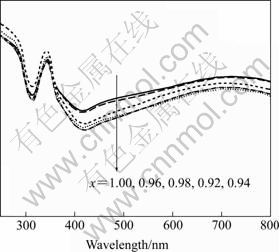
ͼ4 CuxAlO2�մɵ�UV-Vis ���չ���
Fig.4 UV-Vis of CuxAlO2 ceramics
2.4 �մɵĵ�ѧ����
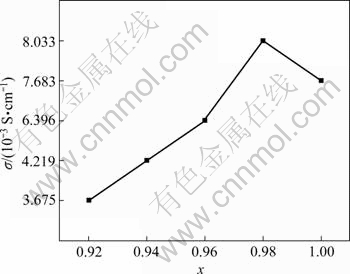
��ͬ��ѧ�����ȵ��մ���Ʒ�������µĵ���������ͼ5��ʾ����ͼ�п��Կ���������xֵ��������Ʒ�����µ絼������������С���������ܶȱ仯������ȫһ�¡�x=0.98ʱ���õ���һϵ����Ʒ�絼�ʵ����ֵ8.03��10?3 S/cm����������Ʒ�絼�����¶�(100~300 K)�ı仯��������ı仯������x=0.98ʱΪ������ͼ6��ʾ���絼�����¶ȵ����߶�����������������100~300 K֮��ܺõط���Arrhenius[15]��ϵʽ��
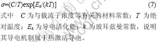
ͼ5 CuxAlO2�մɵ����µ絼��
Fig.5 Electrical conductivity of CuxAlO2 ceramics at room temperature
ͼ6 CuxAlO2 (x=0.98)�մɵ絼�����¶ȵı仯
Fig.6 Electrical conductivity of CuxAlO2 (x=0.98) ceramics dependence of temperature
����ln �ҡ�T ?1��ϵ�������Ʒ���ȼ�����(��ͬ�����Ʒ���ȼ����ܵ�ֵ��0.085~0.147 eV֮��)��x=0.98ʱ��������ͣ���Ϊ0.085 eV�����������մ����ܶ���絼����xֵ�仯���ɵ�һ���ԣ�������Ϊ��CuAlO2�մɵĵ������ܱ仯��Ҫ�����մ�Ƭ�����ܶȾ����ġ������մ������Ե����ӣ����������Ͻ���, �������Ӵ������谭���õĿ�϶��Ŀ����, ʹ�������ӵ�Ǩ�Ƹ�Ϊ���������ӵ�Ǩ�������ӣ��Ӷ�����CuAlO2�մɵ絼������������
3 ����
1) ���ù����սᷨ�Ʊ��˲�ͬ��ѧ�����ȵ�CuxAlO2�մɣ���XRD�ױ�������x=1.0ʱ����Ʒ�а�����������CuO���ɣ�������ֶ��õ��˽ϴ����ͭ����ṹ�����ܶ���xֵ������������ҵ�x=0.98ʱ�õ���һϵ���е����ֵ5.02 g/cm3��CuxAlO2�մɵ�SEM��ͬʱҲ֤������Ʒ���ܶ���xֵ�仯����һ���ɡ�
2) ͨ������Ʒ����UV-Vis ���չ��ײ��ԣ��õ���Ʒ�Ĺ�ѧ��϶���Ⱦ�ԼΪ3.44 eV��x=0.98ʱ��CuxAlO2�մ�ϵ�������ĵ絼��8.03��10?3 S/cm��
3) ��100~300 K��Χ�ڣ��絼�ʵı仯���ɺܺõط���Arrhenius��ϵ��������x=0.98ʱ���õ���ϵ����С������0.085 eV��
REFERENCES
[1] Kawazoe H, Yasukawa M, Hyodo H, Kurita M, Yanagi H, Hosono H. P-type electrical conduction in transparent thin films of CuAlO2[J]. Nature, 1997, 389: 939?942.
[2] Thomas G. Invisible circuits[J]. Nature, 1997, 389: 907?908.
[3] Zhu F R, Zhang K, Low B L, Lim S F, Chua S J. Morphological and electrical properties of indium tin oxide films prepared at a low processing temperature for flexible organic light-emitting devices[J]. Materials Science and Engineering B, 2001, 85: 114?117.
[4] Craciun V, Craciun D, Wang X, Anderson T J, Singh R K. Highly conducting indium tin oxide films grown by ultraviolet-assisted pulsed laser deposition at low temperatures[J]. Thin Solid Film, 2004, 453/454: 256?261.
[5] Zhu F R, Zhang K, Guenther E, Chua S J. Optimized indium tin oxide contact for organic light emitting diode applications[J]. Thin Solid Film, 2000, 363: 314?317.
[6] Banerjee A N, Maity R, Ghosh P K, Chattopadhyay K K. Thermoelectric properties and electrical characteristics of sputter-deposited p-CuAlO2 thin films[J]. Thin Solid Films, 2005, 474: 261?266.
[7] Gong H, Wang Y, Luo Y. Nanocrystalline p-type transparent Cu-Al-O semiconductor prepared by chemical-vapor deposition with Cu(acac)2 and Al(acac)3 precursors[J]. Applied Physics Letters, 2000, 76: 3959?3961.
[8] Banerjee A N, Chattopadhyay K K. Size-dependent optical properties of sputter-deposited nanocrystalline p-type transparent CuAlO2 thin films[J]. Journal of Applied Physics, 2005, 97: 84308?84315.
[9] Tonooka K, Shimokawa K, Nishimura O. Properties of copper�Caluminum oxide films prepared by solution methods[J]. Thin Solid Films, 2002, 411: 129?133.
[10] Bouzidi C, Bouzouita H, Timoumi A, Rezig B. Fabrication and characterization of CuAlO2 transparent thin films prepared by spray technique[J]. Materials Science and Engineering B, 2005, 118: 259?263.
[11] ����. �ſؽ��似����չ��Ӧ��(��)[J]. �ִ�����, 2005, 5: 1?5.
XU Wan-jing. Recent developments and applications in magnetron sputtering[J]. Modern Instrument, 2005, 5: 1?5.
[12] Ishiguro T, Kitazawa A, Mizutani N, Kato M. Single-crystal growth and crystal structure refinement of CuAlO2[J]. J Solid State Chem, 1981, 40: 170?174.
[13] �Դ���, Ҧ Ϊ. P��CuAlO2 �뵼���մɵ��ս��о�[J]. ��ĩұ����, 2004, 22: 333?336.
ZHAO Da-qing, YAO Wei. P-type CuAlO2 semiconductor ceramic material prepared by sintering[J]. Powder Metallurgy Technology, 2004, 22: 333?336.
[14] ������, ��ΰ��, ������, ������, �����. ���ܸ������ӵ����մ�SrCe0.9Y0.1O3?�����Ʊ�[J]. �й���ɫ����ѧ��, 2006, 16(6): 1046?1051.
WU Min-yan, DING Wei-zhong, FANG Jian-hui, ZHANG Yu-wen, MA Jin-chang. Preparation of dense high temperature proton conducting ceramics SrCe0.9Y0.1O3�C�� [J]. The Chinese Journal of Nonferrous Metals, 2006, 16(6): 1046?1051.
[15] Stevenson J W, Armstrong T R, Carneim R D, Pederson L R, Weber W J. Electrochemical properties of mixed conducting perovskites La1?xMxCo1?yFeyO3?�� (M= Sr, Ba, Ca) [J]. J Electrochem Soc, 1996, 143: 2722?2729.
������Ŀ��������Ȼ��ѧ����������Ŀ(60576012)
�ո����ڣ�2006-10-16�������ڣ�2007-06-25
ͨѶ���ߣ��� ���������ڣ��绰��010- 67392733��E-mail: mzhang@bjut.edu.cn
(�༭������Ⱥ)
