Article ID: 1003-6326(2005)02-0306-04
Synthesis and characterization of
single-crystalline alumina nanowires
ZHAO Qing(�� ��), XU Xiang-yu(������), ZHANG Hong-zhou(�ź���),
CHEN Yao-feng(��ҫ��), XU Jun(�� ��), YU Da-peng(�����)
(School of Physics, State Key Laboratory for Mesoscopic Physics, Peking University, Beijing 100871, China)
Abstract: Alumina nanowires were synthesized on large-area silicon substrate via simple thermal evaporation method of heating a mixture of aluminum and alumina powders without using any catalyst or template. The phase structure and the surface morphology of the as-grown sample were analyzed by X-ray diffractometry(XRD) and scanning electron microscopy(SEM), respectively. The chemical composition and the microstructure of the as-grown alumina nanowires were characterized using transmission electron microscope(TEM). The nanowires are usually straight and the single crystalline has average diameter of 40nm and length of 3-5��m. The growth direction is along the [002] direction. Well aligned alumina nanowire arrays were observed on the surface of many large particles. The catalyst-free growth of the alumina nanowires was explained under the framework of a vapor-solid(VS) growth mechanism. This as-synthesized alumina nanowires could find potential applications in the fabrication of nanodevices.
Key words: alumina nanowires; vapor-solid growth; nanomaterials CLC number: O488
Document code: A
1 INTRODUCTION
In recent years, exclusive attention has been focused on one-dimensional nanomaterials due to their peculiar structures and properties useful both for fundamental physics research and potential applications in electronic, optical, magnetic, and nanoscale devices[1-4]. It is imperative to synthesize oriented nanostructure arrays in order to achieve high quality function and evaluate the related physical properties of the nanodevices. Some nanostructure arrays such as shape-controllable ZnO nanorod arrays[5], highly ordered boron nanowire arrays[6], ordered GaAs nanowire arrays[7] have been fabricated recently via different methods. However, synthesis of well-aligned nanostructures with desirable dimensionalities and ordered assemblies is still a major challenge from material synthesis point of view. Al2O3, a good traditional structural ceramic material, nowadays is proved to be valuable in nano science and technology due to its special properties such as high elastic modulus, thermal and chemical stability, high strength and toughness[8]. Alumina whiskers and fibers are widely used in metal matrix composites[9], catalyst supports, radar transparent structures and antenna windows[10]. Alumina nanostructures can also find potential applications in high-temperature composite materials in nanodevices. Different methods have been reported in the fabrication of alumina nanostructures, such as thermal evaporation using iron as catalyst to grow Al2O3 nanowires and nanotrees[11]; in situ catalytic growth of Al2O3 nanowires by heating a mixture of Al, SiO2 and Fe2O3 catalyst[12]; synthesis of alumina nanotubes using carbon nanotubes as templates[13]; fabrication of branchy alumina nanotubes by in situ stepwise electrochemical anodization of Al/Si in dilute sulfuric acid[14]. Recently, the alumina nanostructure arrays have also been reported. Yuan et al[15] reported the fabrication of regular alumina nanopillar arrays by simple chemical etching of the ordered porous alumina film on an aluminum surface. Pang et al[16] used direct electrodeposition in the nanochannels of anode alumina membranes to fabricate alumina nanowire arrays. These methods all employed the so-called template growth with relative long and complicated process, and the resultant nanowires are amorphous in nature. What is more, most of the previous reports on synthesizing alumina nanowires[11, 12] follow the conventional VLS mechanism[17], in which eutectic alloy droplets composed of metal catalysts (usually Fe, Ni or Au) and target materials are necessary. The catalyst impurities would be easily solved into the target materials during the growth process and they will seriously influence the physical performance of the target materials as a result. Therefore, it is necessary to synthesize alumina nanowire arrays through a simple way without using catalyst or template. In the present work, a simple vapor deposition method was introduced to fabricate large-area pure and oriented crystalline Al2O3 nanowire arrays without involvement of any catalyst impurity. The method developed in this work offers an efficient and rational approach for the low cost and large-scale synthesis of a diverse variety of other high ordered nanostructures.
2 EXPERIMENTAL
A very simple physical vapor deposition method was employed in this work to prepare the oriented Al2O3 nanowires. Aluminum powder (99.9%) and alumina powder (99.9%) with molar ratio of 25��1 were mixed together and put in an alumina boat. Then a clean 1cm2 silicon substrate was placed on the boat. The boat was placed into a quartz tube in a horizontal tube furnace with the boat located at the center of the tube. The system was then vacuumed by a mechanical pump to about 20kPa and maintained at this vacuum during the whole growth process. The furnace was heated at a rate of 20��/min to 1000�� and maintained for 120min under continuous argon flow of 100mL/s. After the furnace cooled down, a white fluffy layer was covered the surface of the silicon substrate. X-ray diffraction technique was first carried out to investigate the phase structure of the products. A field emission Strata DB235-FIB working at scanning microscope mode was used to observe the surface morphology of the sample. A Tecnai F30 microscope operating at 300kV with field emission gun and energy dispersive spectroscopy(EDS) detector was employed to analyze the microstructure and chemical composition of the sample.
3 RESULTS AND DISCUSSION
The X-ray diffraction pattern of the as-prepared product is shown in Fig.1. The pattern is attributable to the orthorhombic Al2O3 phase with cell constants of a=4.843�@, b=8.330�@ and c=8.954�@. Two peaks corresponding to Si substrate are also marked. No diffraction peaks from Al have been found in our sample, indicating the high purity of the sample.

Fig.1 XRD pattern of as-prepared sample
Fig.2(a) is a typical SEM image of the products, showing that entangled and uniform alumina nanowires were formed on the entire substrate (about 1cm2) area in high yield. The nanowires are usually straight and uniform along their entire length. The nanowires are 40nm wide and 5-7��m long on the averge. The substrate was covered with this kind of nanowires uniformly and compactly. In some areas, well-aligned nanowire arrays are observed on some big particles, which is demonstrated in Fig.2(b). Fig.2(c) is the magnified image showing that the nanowires on the surface of the big particle are highly oriented and well aligned. They grown perpendicular to the surface of the big particles. The densely aligned alumina nanowires cover the whole particle surface and tend to form the closest packing. This kind of oriented nanowire arrays is in high density and can easily be found in the as-grown products.

Fig.2 SEM images of products
The chemical composition and the microstructure were analyzed by TEM technique. The energy dispersive spectroscopy(EDS) of one representative individual nanowire shown in Fig.3(a) reveals that the nanowire is composed of Al and O elements, confirming the chemical composition of the as-grown nanowires. Cu and C peaks come from the TEM grid. Fig.3(b) shows a high-resolution TEM (HRTEM) image of a single alumina nanowire. One set of the lattice plane is found parallel to the axis of the wire. The spacing of 0.447nm between adjacent lattice planes corresponds to the distance between two (002) crystal planes of orthorhombic Al2O3, indicating that [002] is the growth direction for the as-synthesized nanowires. Obviously, the alumina nanowires are structurally uniform single crystalline with high crystal quality. No particle was observed at the end of the nanowires. The synthesis way is simple without using catalyst, which is necessary in many other methods. What��s more, the method is template-free.
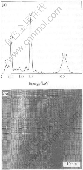
Fig.3 EDS spectrum of single alumina nanowire(a) and HRTEM image of one typical nanowire(b)
The classic vapor-liquid-solid(VLS) mechanism is not suitable to explain the formation mechanism of the nanowires in our case because no catalyst is used in this work. A vapor-solid(VS) model is taken to explain the growth mechanism of the alumina nanowires in this paper. Two chemical reactions take place when the furnace temperature reaches 1000��, which are shown as follows:
Al(l)+Al2O3(s)��Al2O(g)(1)
Al2O(g)+O2(g)��Al2O3(s)(2)
Because the melting point of Al (660��) is lower than 1000�� while its boiling point (2467��) is much higher, aluminum in liquid phase continuously reacted with the solid alumina powder (melting point: 2054��) to form Al2O vapor as reaction (1). The formed metastable Al2O vapor acted as self-catalyst, and it is easily oxidized by the residual oxygen in the system, finally forming the nuclei of the Al2O3 nanowires deposited on the silicon substrate. During the long heating process at 1000��, more Al atoms were evaporated to react with alumina, and the nuclei grew along the preferential [002] direction to form the alumina nanowires.
The formation of the oriented nanowire arrays on many big particles (shown in Figs.2(b) and (c)) can be explained as follows. Some big particles (with diameter of 10��m) were first deposited on the silicon substrate which provided favorite nucleation sites on their surfaces. The very high density of nuclei formed on the surface of one big particle makes the crowd effect very significant, and as a result, the interaction force between individual nanowire seeds keeps them grow in arrays. Adding a small quantity of alumina powder in the source materials can improve the growth process. The small amount alumina in the source materials can help to form the Al2O vapor which is the most important factor in the nano alumina crystal nucleation process in the framework of the VS growth mechanism.
4 CONCLUSIONS
Alumina nanowires were synthesized on large-area substrate via a very simple thermal evaporation method without involving any catalyst or template. The nanowires are about 40nm in diameter and 5-7��m in length with high yield. Arrays of alumina nanowire were found grown on the surface of many large particles. The nanowires are of good single crystalline quality and high purity. They all grow along the [002] direction of alumina. A VS model is used to explain the possible growth mechanism of the alumina nanowires, which is different from most of the other synthesis methods. This method offers an efficient way to synthesize other nanostructures. Large-scale alumina nanowire arrays with good uniformity are especially appropriate for practical applications such as nano mechanical device systems.
REFERENCES
[1]Duan X F, Huang Y, Cui Y, et al. Indium phosphide nanowires as building blocks for nanoscale electronic and optoelectronic devices [J]. Nature, 2001, 409: 66-69.
[2]Yu D P, Bai Z G, Wang J J, et al. Direct evidence of quantum confinement from the size dependence of the photoluminescence of silicon quantum wires [J]. Phys Rev B, 1999, 59(4): R2498-R2501.
[3]Chang Y Q, Wang D B, Luo X H, et al. Synthesis, optical, and magnetic properties of diluted magnetic semiconductor Zn1-xMnxO nanowires via vapor phase growth [J]. Appl Phys Lett, 2003, 83(19): 4020-4022.
[4]Cui Y, Lieber C M. Functional nanoscale electronic devices assembled using silicon nanowire building blocks [J]. Science, 2001, 291: 851-853.
[5]Sun X C, Zhang H Z, Xu J, et al. Shape controllable synthesis of ZnO nanorod arrays via vapor phase growth [J]. Solid State Comm, 2004, 129: 803-807.
[6]Cao L M, Hahn K, Scheu C, et al. Template-catalyst-free growth of highly ordered boron nanowire arrays [J]. Appl Phys Lett, 2002, 80(22): 4226-4228.
[7]Wu Z H, Mei X Y, Kim D, et al. Growth of Au-catalyzed ordered GaAs nanowire arrays by molecular-beam epitaxy [J]. Appl Phys Lett, 2002, 81(27): 5177-5179.
[8]Yu Z Q, Du W W. Preparation of nanometer-sized alumina whiskers [J]. J Mater Res, 1998, 13: 3017-3018.
[9]Dragone T L, Nix W D. Steady state and transient creep properties of an aluminum alloy reinforced with alumina fibers [J]. Acta Metall Mater, 1992, 40(10): 2781-2791.
[10]Cooke T F. Inorganic fibers��a literature review [J]. J Am Ceram Soc, 1991, 74: 2959-2978.
[11]Zhou J, Deng S Z, Chen J, et al.Synthesis of crystalline alumina nanowires and nanotrees [J]. Chem Phys Lett, 2002, 365: 505-508.
[12]Tang C C, Fan S S, Li P, et al. In-situ catalytic growth of Al2O3 and Si nanowires [J]. J Cryst Growth, 2001, 224:117-121.
[13]Zhang Y J, Liu J, He R R, et al. Synthesis of alumina nanotubes using carbon nanotubes as templates [J]. Chem Phys Lett, 2002, 360: 579-584.
[14]Zou J P, Pu L, Bao X M, et al. Branchy alumina nanotubes [J]. Appl Phys Lett, 2002, 80(6):1079-1081.
[15]Yuan Z H, Huang H , Fan S S. Regular alumina nanopillar arrays [J]. Adv Mater, 2002, 14(4): 303-305.
[16]Pang Y T, Meng G W, Zhang L D, et al. Electrochemical synthesis of ordered alumina nanowire arrays [J]. J Solid State Electrochem, 2003, 7: 344-347.
[17]Wager R S, Ellis W C. Vapor-liquid-solid mechanism of single crystal growth [J]. Appl Phys Lett, 1964, 4(5): 89-90.
Foundation item: Projects(50025206; 20151002) supported by the National Natural Science Foundation of China; Project(2002CB613505) supported by the National Key Fundamental Research Program of China
Received date: 2004-11-15; Accepted date: 2005-01-18
Correspondence: YU Da-peng, Professor; Tel: +86-10-62759474; Fax: 86-10-62759474; E-mail: yudp@pku.edu.cn
(Edited by LONG Huai-zhong)

