
Manipulation of space charge in silicon by intentional
thermal donor activation
E. TUOVINEN, J. H?RK?NEN, P. LUUKKA, E. TUOMINEN
Helsinki Institute of Physics, University of Helsinki, Finland 00014
Received 20 April 2006; accepted 30 June 2006
Abstract: A quantitative study about the thermal activation of thermal donors (TD) in high resistivity magnetic Czochralski (MCz) silicon was carried out. The samples are p+/p/n+ diodes (active area 0.25 cm2, thickness 300 ��m) made of <100> MCz p-type Si wafers with the resistivity of about 2 k��?cm. The concentration of interstitial oxygen (Oi) in this material was measured by the Fourier transformation infrared (FTIR) spectroscopy method and it is 4.9��1017 cm-3. The TD activation was performed through an isochronal thermal treatment at 430 �� up to a total time of 120 min. The space charge density after each annealing step was extracted from capacitance-voltage (CV) measurements. The TD generation can be utilized in processing of silicon detectors (pixel, strip and drift detectors) that are used e.g. in space applications, high-energy physics experiments, and several visual imaging applications. If the starting material is boron-doped p-type high-resistivity Cz-Si, the TD generation process can be utilized in order to produce p+/n-/n+ detectors. The last thermal process step, i.e. the sintering of aluminum, is intentionally carried out at the temperature where TD��s are created. Due to the generated donors, the p-type bulk will eventually be compensated to n-type bulk. Moreover, the full depletion voltage of detectors (Vfd) could be tailored between a wide range from 30 V up to almost 1 000 V by changing heat treatment duration at 400-450 �� from 20 to 120 min.
Key words: thermal donor; silicon; particle detector; radiation defect
1 Introduction
It is well known that the aggregation of oxygen atoms leads to formation of electrically active defects, commonly named thermal donors (TD) [1, 2]. The TD��s are probably among the most studied defects in semiconductors. The TD��s are shallow donor levels within 0.01-0.2 eV energy range below the conduction band [3]. The formation of thermal donors depends strongly on the temperature and the oxygen concentration in the silicon material. A heat treatment between 400 and 600 �� can yield a TD concentration comparable with the initial doping concentration in the high resistivity silicon. The formation of the TD��s has often been explained to be due to the so called anomalously fast diffusing species (FDS). Oxygen dimers (O2) and trimers (O3) among other oxygen complexes have been proposed to be such FDS��s [4]. Additionally, a fourth-power dependence of the thermal donor generation rate (d/dt NTD) on the oxygen concentration has widely been quoted.
The purpose of this work is to characterize and model the TD formation in high resistivity magnetic Czochralski (MCz) silicon material. The motivation arises from the lately developed application of the MCz as very radiation hard particle detector material for high energy physics (HEP) applications. The sensors used in particle tracking systems must be fully depleted at reasonably low operating voltages, typically less than 100 V. Therefore, the silicon sensors have traditionally been fabricated on wafers made by float zone (Fz-Si) crystal growth technique. Fz-Si technique ensures high-purity and sufficiently defect-free silicon crystals that are the basic requirements for producing high-resistivity silicon substrates for detector applications. On the other hand, Fz-Si has characteristically a low oxygen concentration because of the contact-less, crucible-free crystal growth technique. Low oxygen concentration in Fz-Si is a drawback for radiation hardness [5, 6].
Although the Cz-Si is the basic raw material for microelectronics industry, high resistivity (��1 k��?cm) MCz-Si wafers suitable for detector fabrication have become available only recently [7]. During the crystal growth, oxygen is dissolved into silicon from the quartz crucible. A major part of the oxygen is dissolved as silicon monoxide and is flushed away by argon gas. Furthermore, the resulting oxygen concentration depends on the velocity of the silicon melt flow as well as on the rate of the oxygen evaporation from the surface of the melt. These parameters can be influenced in order to get the desired oxygen concentration in the silicon ingot. The application of a magnetic field is an especially effective way to moderate and to control the melt flow since the silicon melt is an electrically conductive liquid [8].
In this paper, a detector fabrication process, measurement and characterization of TD��s in MCz-Si substrates were described, an empirical model for TD formation was proposed and the benefit and applications of TD��s in particle detectors were discussed.
2 Samples
All samples used in this study have been processed on p-type magnetic Czochralski silicon wafers (MCz-Si) [8]. The starting material of the detectors was 4�� diameter double-side-polished (300��2) ��m thick <100> Cz-Si wafers. The nominal resistivity, measured by the four point probe method, of the boron-doped wafers is 1 800 ��?cm, which corresponds to a boron concentration of 4.38��1012 cm-3. The oxygen concentration of these wafers was measured by the Fourier transformation infrared (FTIR) spectroscopy. The measurements were done on a thick reference wafer at the Institute of Electronic Materials Technology (ITME), Warszawa, Poland. The following oxygen concentrations were measured: 4.95��1017 cm-3 (center), 4.89��1017 cm-3 (right), 4.93��1017 cm-3 (left) and 4.93��1017 cm-3 (bottom).
Two types of pad detectors were processed at the Microelectronics Center of Helsinki University of Technology. The active pad implanted area of the diodes is 5 �� 5 mm2. It is surrounded by one wide guard ring (100 ��m) and 16 small guard-rings (each 16 ��m wide). The distance between the active area implant and the first guard ring is 10 ��m. A 1 mm diameter round opening in the front metallization was left for TCT (transient current technique) measurements [9].
The first set of samples were p+/p-/n+ pin-diode structures, i.e. the pad has been implanted by boron and backplane by phosphorous. The second set of samples was n+/p-/p+ structures processed with a different mask set. An additional mask level and boron ion implantation was required because of the electron accumulation at the SiO2/Si surface. The surface inversion was terminated by boron implanted guard rings. One 100 ��m wide and eight 16 ��m wide guard rings were processed between the n+ rings. Boron field implantation (often referred as p-spray) was not done for these samples. The process contains three thermal oxidations. The oxidations were done at 1 100 ��. After the oxidations, the temperature was ramped down at the rate 4 ��/min. The pull-out of the wafers took place at the 700 ��. Thus the wafers were cooled as fast as possible in order to avoid TD formation temperature range 400-600 ��. All detectors were passivated by approximately 60 nm thick silicon nitride (Si3N4) film grown by plasma enhanced chemical vapor deposition (PECVD) method. The deposition temperature of PECVD Si3N4 is 300 ��.
The last process step of these detectors was aluminum sintering. In order to study the thermal donor generation, the detector wafers were sintered at 430 �� for different times, i.e. 35, 45, 60, 70 and 80 min, at the peak temperature. The thermal profile of the sintering is push-in in 2 min followed by the 10 min stabilation while the furnace settles again at the peak temperature (the furnace door is open during the push-in). After heating at the peak temperature the wafers were pulled-out in 2 min. An n+/p-/p+ reference wafer was processed and sintered at 370 ��.
After processing, the wafers, containing 80 pad detectors each, were diced. The diodes were characterized at the probe station by capacitance-voltage (CV) and current-voltage (IV) measurements.
The formation of the thermal donors depends not only on the oxygen concentration, but also on the temperature and on the amount of hydrogen used in the detector manufacturing process [10]. In order to study the spatial uniformity of the full depletion voltage, Vfd, ten diodes along the wafers diameter were picked for the CV measurements, as shown in Fig 1.
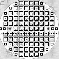
Fig.1 Position on wafer of pad detectors used in this study
3 Measurements
When a detector is reversed biased, the electric field extends towards the backplane of the detector. With sufficiently high reverse bias, the space charge region exists through the entire bulk, i.e. the detector is fully depleted and the capacitance signal saturates. The full depletion voltage (Vfd) of the devices was extracted from the CV curve measured at the room temperature and at 10 kHz frequency. The effective doping concentration (Neff) is calculated from Eqn.(1).
 (1)
(1)
where d is the thickness of the detector, q is the elementary charge, �� is the dielectric constant of the silicon. The concentration of TD��s is obtained from Eqn.(2).

 (2)
(2)
where NA is the boron doping concentration of the wafers. The value NA = 7.38��1012 cm-3 was obtained from the depletion of as-processed p-type devices that took place at 300 V. It corresponds to a resistivity of approximately 3 000 ��?cm, which differs from the 1 800 ��?cm value provided by the wafer manufacturer. It is therefore obvious that boron doping has been to some extent compensated during the detector processing.
4 Results and modeling of TD formation
The results of the CV measurements are shown in Fig 2. The sign of the space charge is obtained from TCT measurements reported in Ref.[11].
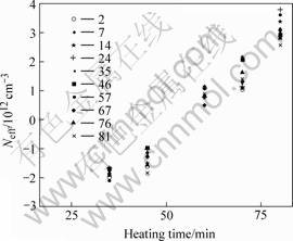
Fig.2 Effective doping concentration (Nff) with respect heating time at 430 ��. The individual symbols correspond to the diode numbering presented in Fig.1
It can be seen that the TD formation is almost linear. It is therefore obvious that the empirical models, claiming third-power dependence on the oxygen concentration, proposed in Ref.[2, 12], cannot explain our experimental results. We have made an effort to improve the existing models by following the time and temperature depended equation with two fitting parameters.
 (3)
(3)
where t is the time, T is the absolute temperature and a is given by:
 (4)
(4)
where c is a fitting constant, Oi is the concentration of the interstitial oxygen and the �� is the reaction order, i.e. the exponent to where oxygen concentration is to be raised.
The x in Eqn.(3) is given by:
 (5)
(5)
where b is a fitting parameter and Di is the diffusion coefficient of the interstitial oxygen given by:
 (6)
(6)
where k is the Bolzmann��s constant and EA is the activation energy, EA=2.53 eV, which value is found in Ref.[2]. The fitting of the model to the experimental data is shown in Fig.3.
Fig.3 Exponential fit of proposed model to experimental data. The data points correspond to the average of the measurements of Neff
The fitting gives following results:

5 Conclusions
There is a good agreement between the calculations of the Eqns.(1)-(6) and the experimental data, based on measurement of Vfd, if the TD generation is assumed to obey NTD?Oi.1.89 dependence on the oxygen concentration. In the literature, a fourth-power dependence of the thermal donor generation rate (d/dtNTD) on the oxygen concentration has widely been quoted. The fourth-power reaction order assumption for the generation rate has generally been accepted to be evidence that the core of the TD defect consists of four oxygen atoms. There are, however, experimental observations based on the infrared absorption method that claim strong deviations from the fourth-power dependence, which originally was established to be TD generation at 450 �� [12]. With lower temperatures, at e.g. 430 ��, the exponential dependence in the formation has been reported to be very close to our finding 1.83. Additionally, LEE et al have shown by total energy calculations in [13, 14] that the TD formation is not due to the so called fast diffusing species (FDS) and report a reaction order close to 2.
As described in the introduction, there is technological importance in TD��s. The shallow donors have twofold influence on the macroscopic properties of the detectors. First, shallow oxygen thermal donors can be utilized during the fabrication process in order to manipulate the effective doping concentration (Neff) of the silicon bulk [15]. This is important in order to tailor the full depletion voltage (Vfd). Second, the shallow donors interact with the radiation defects and influence the radiation hardness of the detectors [16]. With TD generation method, it is possible, with low cost and with a process of low thermal budget, to fabricate detectors with high oxygen concentration that can be depleted at voltages less than 100 V.
References
[1] OEHRLEIN G S. Silicon�Coxygen complexes containing three oxygen atoms as the dominant thermal donor species in heat-treated oxygen-containing silicon[J]. J Appl Phys, 1983, 54: 5453.
[2] WADA K. Unified model for formation kinetics of oxygen thermal donors in silicon[J]. Phys Rev B, 1984, 10: 5884.
[3] OURMAZD A, et al. Oxygen-related thermal donors in silicon: A new structural and kinetic model[J]. J Appl Phys, 1984, 58: 1670.
[4] JONES R. Early Stages of Oxygen Precipitation in Silicon[M]. Dordrecht: Kluwer Academic, 1996.
[5] LINSTROEM G, et al. Radiation hard silicon detectors�� developments by the RD48 (ROSE) collaboration[J]. Nucl Instr and Meth, 2001, A466: 308.
[6] RUZIN A, et al. Comparison of radiation damage in silicon induced by proton and neutron irradiation[J]. IEEE Trans Nucl Sci, 1999, 46(5): 1310.
[7] H?RK?NEN J, et al. Processing of microstrip detectors on Czochralski grown high resistivity silicon substrates[J]. Nucl Instr and Meth, 2003, A514: 173-179.
[8] SAVOLAINEN V, et al. Simulation of large-scale silicon melt flow in magnetic Czochralski growth[J]. J Crystal Growth, 2002, 243(2): 243-260.
[9] EREMIN V, et al. Development of transient current and charge techniques for the measurement of effective net concentration of ionized charges (Neff) in the space charge region of p-n junction detectors[J]. Nucl Instr and Meth, 1996, A372: 188.
[10] SIMOEN A, et al. Hydrogen plasma-enhanced thermal donor formation in n-type oxygendoped high-resistivity float-zone silicon[J]. Appl Phys Lett, 2002, 81(10): 1842.
[11] H?RK?NEN J, et al. p+/n-/n+ Cz-Si detectors processed on boron doped substrates with thermal donor induced space charge sign inversion[J]. IEEE Trans Nucl Sci, 2005, 52: 1865-1868.
[12] WIJARANAKULA W. Formation kinetics of oxygen thermal donors in silicon[J]. Appl Phys Lett, 1991, 59(13): 1608.
[13] LEE Y J, et al. First-principles study of migration, restructuring, and dissociation energies of oxygen complexes in silicon[J]. Phys Rev B, 2002, 65: 085205.
[14] LEE Y J, et al. Simulation of the kinetics of oxygen complexes in crystalline silicon[J]. Phys Rev B, 2002, 66: 165221.
[15] H?RK?NEN J, et al. Proton irradiation results of p+/n-/n+ Cz-Si detectors processed on p-type boron-doped substrates with thermal donor-induced space charge sign inversion[J]. Nucl Instr and Meth, 2005, A552: 43-48.
[16] PINTILIE I, et al. Stable radiation-induced donor generation and its influence on the radiation tolerance of silicon diodes[J]. Nucl Instr and Meth, 2006, A556: 197-208.
(Edited by YANG Hua)
Corresponding author: E. TUOVINEN; Tel: +358-9-4512365; Fax: +358-9-4516080; E-mail: esa.tuovinen@helsinki.fi

