TiO2���ܱ�Ĥ���Ѳ�����
��Դ�ڿ����й���ɫ����ѧ��(Ӣ�İ�)2012���11��
�������ߣ����� WANG Ri-zhi
����ҳ�룺2691 - 2699
�ؼ��ʣ�TiO2���ܣ��������ǿ�ȣ��Ѳ���Ϊ���Ѳ��ܶȣ��Ѳ�뾶���ڲ���Ӧ��
Key words��TiO2 nanotube; interfacial shear strength; debonding behavior; debonding density; debonding radius; internal residued stress
ժ Ҫ���ֱ�ͨ�����ʷ��ͻ�������Ӧ����Է����о�TiO2���ܱ�Ĥ�IJ���Ӧ�����Ѳ���Ϊ�����������TiO2���ܱ�Ĥ���ڲ���Ӧ��Ϊ-54 MPa��TiO2���ܱ�Ĥ��������250 ��C�˻�����400 ��C�˻������Ѳ���ֵ��Ӧ������Ϊ2.6%��5.1% ��8.6%���뾶����Ϊ27.5��17.1��19.4 ��m��TiO2���ܱ�Ĥ��������250 ��C�˻�����400 ��C�˻�������ʵ�ٽ��Ѳ�Ӧ��Ϊ220.4��394.5��627.9 MPa�����Ѳ������£��Խ������ģ�ͽ�����������TiO2���ܱ�Ĥ�������ǿ�Ƚ��ж���ʽ��ϡ�������Ͻ���������ܶȵķ�������ܺܺ��Ǻϣ���˽������ģ�͵������̺Ͷ���ʽ��Ϸ��̾�Ϊ���ŵġ�
Abstract: Curvature method was used to measure the residual stress and substrate straining tensile test was carried out to study the debonding behavior of TiO2 nanotube film. The results indicate that the internal residual stress is -54 MPa. The strains of debonding initiation of TiO2 nanotube films without annealing, with 250 ��C annealing and with 400 ��C annealing are 2.6%, 5.1% and 8.6%, respectively, and the average radii of the debonding patches with debonding initiation are 27.5, 17.1 and 19.4 ��m, respectively. The true critical debonding stresses of TiO2 nanotube films without annealing, with 250 ��C annealing and with 400 ��C annealing can be estimated as 220.4, 394.5 and 627.9 MPa, respectively. Interfacial shear lag model is modified and polynomial fitting equation of the interfacial shear strength of TiO2 nanotube film is demonstrated under debonding conditions. The modification and polynomial fitting are reliable since good agreement of the interfacial shear strengths after fitting is obtained compared with those results from the crack density analysis.
Trans. Nonferrous Met. Soc. China 22(2012) 2691-2699
ZOU Jian-peng1, WANG Ri-zhi2
1. State Key Laboratory of Powder Metallurgy, Central South University, Changsha 410083, China;
2. Department of Materials Engineering, University of British Columbia, Vancouver BC, V6T 1Z4, Canada
Received 27 August 2011; accepted 16 November 2011
Abstract: Curvature method was used to measure the residual stress and substrate straining tensile test was carried out to study the debonding behavior of TiO2 nanotube film. The results indicate that the internal residual stress is -54 MPa. The strains of debonding initiation of TiO2 nanotube films without annealing, with 250 ��C annealing and with 400 ��C annealing are 2.6%, 5.1% and 8.6%, respectively, and the average radii of the debonding patches with debonding initiation are 27.5, 17.1 and 19.4 ��m, respectively. The true critical debonding stresses of TiO2 nanotube films without annealing, with 250 ��C annealing and with 400 ��C annealing can be estimated as 220.4, 394.5 and 627.9 MPa, respectively. Interfacial shear lag model is modified and polynomial fitting equation of the interfacial shear strength of TiO2 nanotube film is demonstrated under debonding conditions. The modification and polynomial fitting are reliable since good agreement of the interfacial shear strengths after fitting is obtained compared with those results from the crack density analysis.
Key words: TiO2 nanotube; interfacial shear strength; debonding behavior; debonding density; debonding radius; internal residued stress
1 Introduction
TiO2 nanotubes have attracted more and more attention due to their excellent electronic, photonic, catalytic and gas-sensitive properties [1,2]. They have a great potential in various applications such as photocatalysis [3,4], solar energy cell [5,6], environmental purification [7], and gas sensors [8]. Titania nanotubes, and nanotube arrays, have been produced by a variety of methods including deposition into a template [9], sol-gel transcription [10], hydrothermal processes [11] and anodization [12]. TiO2 nanotube films prepared by anodic oxidization have been the subject of intensive research over the past 10 years or so. However, among these nanotube fabrication routes, the most remarkable properties are highly ordered nanotube arrays made by anodization of titanium in fluoride-based baths [13], of which dimensions can be precisely controlled [14].
Debonding is usually encountered between film and substrate due to bonding discontinuities or may be formed due to the dissimilar material properties such as linear thermal expansion or elastic modulus [15]. The combination of the two materials with mismatch of properties across the interface always results in concentration of interfacial stresses, which will lead to initiation of debonding [16]. Many experimental observations of debonding phenomenon have been reported. Residual stress and debonding behavior of DLC coatings have been investigated on the metallic substrates. From knowledge of the residual stress levels in these films as a function of temperature, the release rate of strain energy for interfacial debonding has been monitored during deposition and subsequent temperature changes [17]. The failure by debonding of 400 nm Al thin films on 152 ��m-thick polyimide substrates has been described in uniaxial tension experiments. For a fixed film length, a thinner film will be more unlikely to fail by edge debonding compared with a thicker one [18].
Debonding phenomenon of TiO2 nanotube film has seldom been reported. Based on the previous work on cracking and buckling of TiO2 nanotube film, the debonding research of TiO2 nanotube film was further carried out in this work. After the relationship among debonding radius, debonding density and tensile strain was investigated, the interfacial shear model was modified under debonding conditions. Moreover, the residual stress was measured with curvature method.
2 Experimental
Pure annealed titanium foil (30 mm �� 30 mm, thickness 0.25 mm) bought from Goodfellows Co. was used for tensile test. The Ti foil processing, the TiO2 nanotube fabrication and temperature annealing followed the protocol of our previous studies [19,20]. Tensile test for the TiO2 nanotube coating was carried out on a miniature material testing machine (MINIMAT, Rheometic Scientific Co.). The strain rate was controlled as 0.1 mm/min. An optical microscope was used to observe the debonding behavior of TiO2 nanotube coating. Surface morphology of the tensile specimen was monitored during tensile test by high speed CCD camera with high magnification zoom lens. The image-pro plus software was adopted to measure the debonding radius and density.
3 Results and discussion
3.1 Residual stress measurement of TiO2 nanotube film
The most important methods to measure the residual stress in the films are XRD and curvature methods. Through measuring the changes of the crystal lattice constants, the residual stress can be calculated by XRD. Since the TiO2 nanotube film prepared by anodization is amorphous, there is no possibility to measure the residual stress of TiO2 nanotube film by XRD. On a relatively thin substrate, the residual stress distributed in the coating layer will cause the substrate to bend. The induced curvature for the coated substrate was used to measure the residual stress and depends on the force, the elastic properties as well as the thickness for both substrate and coating.
Titanium foil with thickness of 0.075 mm bought from Goodfellows Co. was specially used to carry out the curvature measurement. To achieve an obvious curvature change, the Ti foil was cut into narrow strips with sizes of 60 mm��3 mm. Wire cutting was used to keep regular and flat planes. Ti foils were cleaned ultrasonically in acetone, absolute ethanol, and distilled water for 15 min sequentially, and then air-dried. In order to calculate the residual stress of the TiO2 nanotube film, one side of the sample should be shielded to prevent the anodic oxidization. The solution was coating one side of the sample with Au powder for 3 min by using Au sputtering apparatus, as shown in Fig. 1. The other side of the sample should face Pt electrode. The fabrication of TiO2 nanotube followed the protocol of our previous studies too [18,19]. The photos of Ti foil sample after anodization are shown in Fig. 2. It can be seen that the curvature change occurred in the Ti foil sample after anodization. Besides, the samples bended towards the Au coating side. So the residual stress in the TiO2 nanotube film was compressive stress. The curvature in Fig. 2(b) can be calculated as -1.2 m-1. The measured curvature difference before and after fabrication of TiO2 nanotube film of the coating (��k) is related to the residual stress (��R) [21]:


where hT is the total thickness of the substrate plus coating; h is the thickness of the coating; ��S is the Poisson ratio of the substrate; Ef is the elastic modulus of the coating and ES is the elastic modulus of the substrate. In this study, Ef, ES, ��S, h and hT are 20 GPa, 120 GPa, 0.32, 4 ��m and 79 ��m, respectively. Thus, the residual stress in the TiO2 nanotube film can be estimated as -54 MPa (in compression).
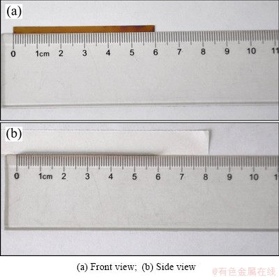
Fig. 1 Photos of Ti foil sample before anodization
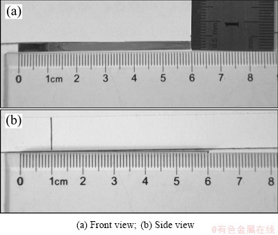
Fig. 2 Photos of Ti foil sample after anodization
3.2 Debonding behavior of TiO2 nanotube film
Debonding dynamics was studied by an optical microscope magnified 100 times and a connecting high speed CCD camera with high magnification zoom lens. Image-pro plus software was used to analyze the debonding area, debonding radius and debonding densities. The radius b of the debonding patch was calculated through b=A/��.
The relationship between debonding density and the strain of the TiO2 nanotube film is shown in Fig. 3. With the increase of tensile strain, the densities of TiO2 nanotube films without annealing, with 250 ��C annealing and with 400 ��C annealing behaved three processes of debonding initiation, propagation and saturation, which demonstrated excellent agreement with the crack density analysis.
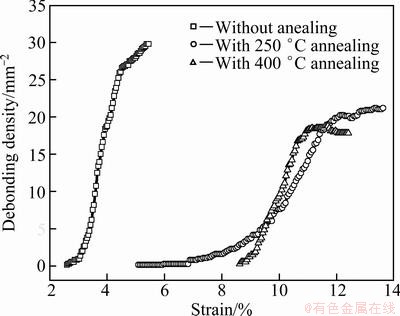
Fig. 3 Relationship between debonding density and strain of TiO2 nanotube film
During the tensile test, the tensile strain is transferred to the TiO2 nanotube film through the interface between the Ti substrate and the TiO2 nanotube film. With the increase of applied axial strain, the tensile stress in the TiO2 nanotube film increases correspondingly. When the stress reaches the critical cracking stress, cracks occur in the TiO2 nanotube film. Once the cracks appear, the cracks propagate abruptly. Thus, crack densities reach saturation within a narrow strain gap. At the same time, axial tensile strain produces transverse compressive strain because of the effect of the Poisson ratio. Transverse compressive stress increases with the increase of tensile strain. When the compressive stress reaches the critical debonding stress, debonding occurs. Similar to the crack propagation model, debonding propagates rapidly once it occurs and reaches the saturation status within a narrow strain gap.
The relationship between the debonding patch radius and the strains of the TiO2 nanotube films without annealing, with 250 ��C annealing and with 400 ��C annealing is shown in Fig. 4. The applied strain has essentially no effect on the minimum size for all the samples. With the increase of strain, the mean debonding patch radii for all the three group samples increase linearly within a small magnitude. The maximum debonding patch radii for 250 ��C annealing samples and 400 ��C annealing samples increase linearly with a large magnitude, while the maximum debonding patch radius for room temperature samples increases exponentially.
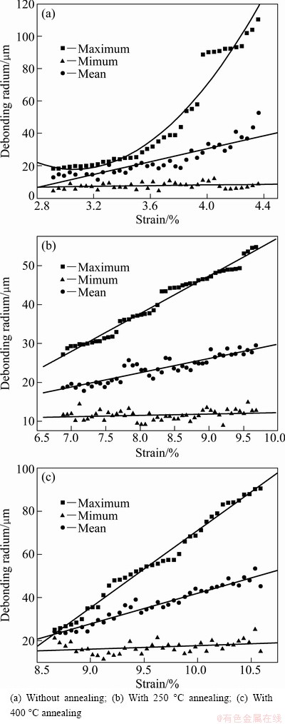
Fig. 4 Minimum, maximum and mean sizes of debonding patches as function of applied strain for TiO2 nanotube film
Merging and incorporation occurred among the debonding patches during the debonding propagation stage, which made the maximum radius of debonding patch increase with a large magnitude. For the room temperature samples, the debonding propagation was the fastest because its interface was the weakest, which made the debonding patch radius increase exponentially. Combining the maximum radius with the almost unchanged minimum radius, mean radius changed with a small magnitude.
The debonding initiation strains of TiO2 nanotube films without annealing, with 250 ��C annealing and with 400 ��C annealing are 2.6%, 5.1% and 8.6%, respectively (Fig. 3) and average radii of the debonding patches with debonding initiation are 27.5, 17.1 and 19.4 ��m, respectively (Fig. 4). The debonding initiation strains of 250 ��C annealing samples and 400 ��C annealing samples are much larger than those of room temperature samples. It can be concluded that annealing has obviously modified the interface between Ti substrate and TiO2 nanotube film. At the same time, the debonding initiation strain of 400 ��C annealing samples is much higher than that of 250 ��C annealing samples, so slightly higher annealing temperature behaves better modifying effect.
3.3 Surface characterization of TiO2 nanotube films
The debonding images of TiO2 nanotube films are shown in Figs. 5-7. The debonding areas appear brighter than the background for room temperature samples (Fig. 5) and darker than the background for 250 ��C annealing samples and 400 ��C annealing samples (Fig. 6 and Fig. 7).
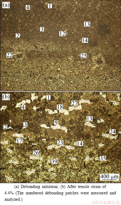
Fig. 5 Debonding images for TiO2 nanotube film without annealing
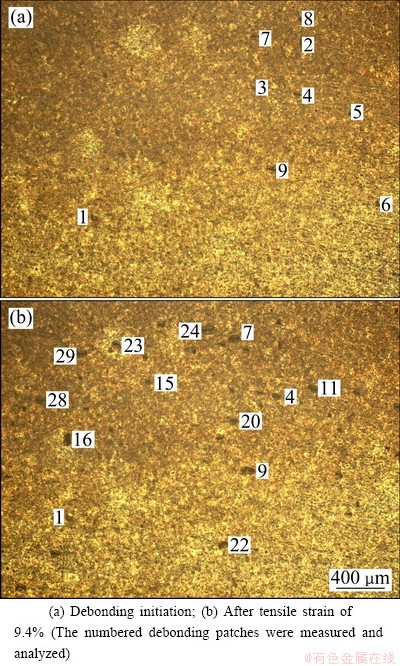
Fig. 6 Debonding images for TiO2 nanotube film with 250 ��C annealing
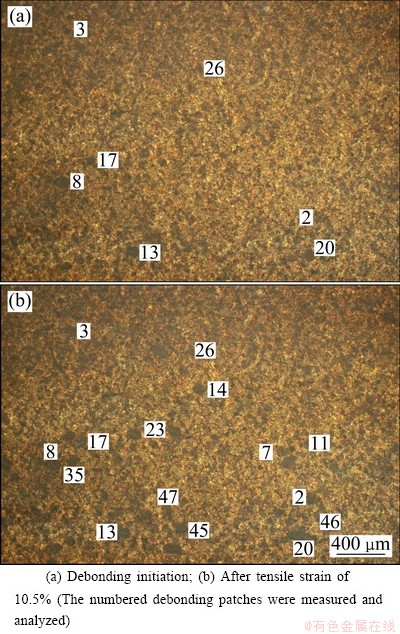
Fig. 7 Debonding images for TiO2 nanotube film with 400 ��C annealing
The possible reason is that debonding patches quickly flake away for room temperature samples (brighter spots left) and debonding patches still cover on the surface of the film for 250 ��C annealing samples and 400 ��C annealing samples (darker spots left). With the increase of the applied strain, debonding density increases.
The radius evolution for the given debonding patches of TiO2 nanotube film without annealing is shown in Fig. 8, which is corresponding to the numbered debonding patches in Fig. 5. With the increase of applied strain, the debonding patch radius of TiO2 nanotube film without annealing experiences three stages of initiation, propagation and saturation, and the propagation stage includes two or three abruptions.
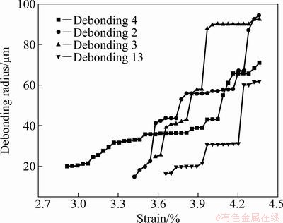
Fig. 8 Radius evolution of given debonding patches with applied strain for TiO2 nanotube film without annealing
The radius evolution for the given debonding patches of TiO2 nanotube film with 250 ��C annealing is shown in Fig. 9, which is corresponding to the numbered debonding patches in Fig. 6. With the increase of applied strain, the debonding patch radius of TiO2 nanotube film with 250 ��C annealing experiences three stages of initiation, propagation and saturation too, and the propagation stage includes one or two abruptions.
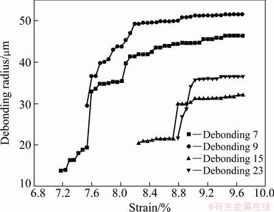
Fig. 9 Radius evolution of given debonding patches with applied strain for TiO2 nanotube film with 250 ��C annealing
The radius evolution for the given debonding patches of TiO2 nanotube film with 400 ��C annealing is shown in Fig. 10, which is corresponding to the numbered debonding patches in Fig. 7. With the increase of applied strain, the debonding patch radius of TiO2 nanotube film with 400 ��C annealing experiences three stages of initiation, propagation and saturation too.
Though the debonding initiation strain was differently, the numbered debonding patches behaved the same tendency of initiation, propagation and saturation with the increase of applied strain. These results demonstrate good agreement with the researches reported by WANG and EVANS [22]. During the tensile test, stress concentration is formed at the interface because of the elastic modulus mismatch between the substrate and the TiO2 nanotube film. Eventually, the film separations occur. The local separation can be regarded as interfacial crack, the crack propagation happens due to the stress concentration of the crack tip. Finally, debonding occurs in the films. Since the debonding propagation energy is far lower than that of the debonding initiation, debonding propagates rapidly once it appears. Thus, the results in Figs. 8-10 can be obtained.
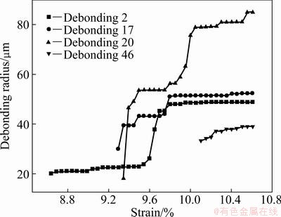
Fig. 10 Radius evolution of given debonding patches with applied strain for TiO2 nanotube film with 400 ��C annealing
3.4 Stresses in TiO2 nanotube film
Transverse compressive strain caused by the axial tensile strain is used to study the debonding dynamics of the TiO2 nanotube film grown on the Ti substrate. Compatibility dictates that the strains in the substrate and the film are the same. Accordingly, upon loading, the axial stress ��X induced in the film is given by [22]
 (1)
(1)
where Ef is the elastic modulus of the film and �� is the applied axial strain. The corresponding transverse stress ��Y is
 (2)
(2)
where �� is Poisson ratio for the substrate. The total stresses are thus
 (3)
(3)
 (4)
(4)
where ��R is the equi-biaxial residual stress, comprising thermal and growth contributions. The thermal residual stress can be calculated as -14.1 MPa and -23.5 MPa for 250 ��C annealing samples and 400 ��C annealing samples, respectively [20]. So, ��R can be estimated as -54, -68.1 and -77.5 MPa for TiO2 nanotube films without annealing, with 250 ��C annealing and with 400 ��C annealing, respectively (in compression).
The debonding process begins when the transverse compressive stress exceeds a critical value ��c. The debonding appears to start randomly, probably due to the presence of defects. The strains of debonding initiation of TiO2 nanotube films without annealing, with 250 ��C annealing and with 400 ��C annealing are found to be 2.6%, 5.1% and 8.6%, respectively. According to equation (4), the true critical debonding stresses ��c of TiO2 nanotube films without annealing, with 250 ��C annealing and with 400 ��C annealing can be estimated as 220.4, 394.5 and 627.9 MPa, respectively. In Ref. [20], the critical buckling stresses of TiO2 nanotube films without annealing, with 250 ��C annealing and with 400 ��C annealing through SEM observation are estimated as 180, 410 and 619.5 MPa, respectively. Excellent agreement of critical debonding stress from optical microscope observation and critical buckling stress from SEM observation has been obtained. It is worth noting that the true strain of debonding initiation can be caught accurately since the debonding photos are given continuously every 4 s (i.e. every 0.07% strain). So, the experimental ��c values obtained above are reasonable.
The crack initiation stresses of TiO2 films without annealing, with 250 ��C annealing and with 400 ��C annealing were calculated as 320, 460 and 900 MPa, respectively [19]. Basically the debonding initiation or the buckling initiation should follow the crack initiation. It seems contradictory since the crack initiation stress is lager than the debonding initiation stress or the buckling initiation stress. But it is not. The reason is that the direction of the debonding initiation stress or the buckling initiation stress is perpendicular to the direction of crack initiation stress. There is no comparability between the crack initiation stress and the debonding initiation stress or the buckling initiation stress.
3.5 Debonding theory and modification
A thin elastic film in compression bonded to a substrate will undergo debonding-driven interfacial delamination when the compressive stress is sufficiently high if an initially debonding patch of interface exists. The film is assumed to be isotropic with elastic modulus (E1), Poisson ratio (��1) and thickness (h). The substrate is also taken to be isotropic but with different moduli, E2 and ��2. The substrate is modeled as being infinitely thick. The stress state in the film is uniform, equi-biaxial compression ��.
When the stress in the film exceeds the critical debonding stress ��c, there is an energy release rate:
 (5)
(5)
where  is the elastic energy per unit area stored in the unbuckled film and
 (6)
(6)
The loading phase angle at the tip of the buckle is given by [23]
 (7)
(7)
where K1 and K2 are the model 1 and model 2 stress intensity factors and
 (8)
(8)
 (9)
(9)
 (10)
(10)
where �� is the thickness of the film; M is the moment; ��N is the effective loading; �� is the phase angle shift.
The criterion for the buckle to propagate is
 (11)
(11)
where ��(��) is the interface toughness and is a function of the loading phase angle ��. A phenomenological representation for ��(��) is [24]
 (12)
(12)
 (13)
(13)
where ��IC is the mode I toughness of the interface (when ��=0). The parameter �� is dependent on the interface roughness.
Interfacial shear lag model is as follows [25,26]:
 (14)
(14)
where �� is the average crack spacing when the crack density becomes constant.
Based on the shear lag model, the interfacial properties including interfacial shear strength, critical energy release rate and fracture toughness can be achieved according to the crack initiation strain and the crack density at the crack saturation strain. Since the cracks are very difficult to be identified with optical microscope and should be observed with SEM, many samples are needed to stop at different strains to catch the crack initiation strain and the saturation strain during tensile test. Sometimes the crack initiation strain and crack saturation strain will be missed if the stopping strains are not selected appropriately. This is a large problem for the shear lag model.
There are no equations relating debonding densities to interfacial properties, especially to interfacial shear strength. If such equations can be developed, it will be a good solution to the problem of shear lag model. Since the debonding photos are taken continuously and the strains change continuously, it will be a convenient method to study the interfacial properties of the films with debonding photos.
Supposing the interfacial shear strength of TiO2 nanotube film can be estimated with equation (14) under debonding conditions, equation (14) can be modified as
 (15)
(15)
where r is the average debonding radius when the debonding initiates.
The average radii of the debonding patch with debonding initiation of TiO2 nanotube films without annealing, with 250 ��C annealing and with 400 ��C annealing are 27.5 ��m, 17.1 ��m and 19.4 ��m, respectively. The true critical debonding stresses of TiO2 nanotube films without annealing, with 250 ��C annealing and with 400 ��C annealing can be estimated as 220.4, 394.5 and 627.9 MPa, respectively. So the interfacial shear strengths �� can be calculated as 67.1, 193.2 and 271.0 MPa, respectively.
The interfacial shear strengths of TiO2 nanotube films without annealing, with 250 ��C annealing and with 400 ��C annealing have been estimated as 163.3, 370.2 and 684.5 MPa, respectively [19]. There is a larger difference between those two groups of data. Polynomial fitting is carried out to figure out the problem and the polynomial regression formula is
 (16)
(16)
According to equation (16), the interfacial shear strengths of TiO2 nanotube film without annealing, with 250 ��C annealing and with 400 ��C annealing are calculated as 164.4, 378.9 and 701.7 MPa, respectively. The modification and polynomial fitting are reliable because excellent agreement of the interfacial shear strengths compared with those results from crack calculation is obtained.
3.6 Synthetical influence of residual stress
It is uncertain how the residual stress in TiO2 nanotube is formed during anodization. There are three possible reasons. First, different coefficients of thermal expansion between Ti substrate and TiO2 nanotube lead to the residual stress in the anodizing preparation process [20]. Second, TiO2 nanotube is grown along the direction perpendicular to the Ti foil plane. Tacking effect is produced at the interface. Besides, the bonding mechanism between TiO2 nanotube and Ti substrate is the strong chemical bonding. TiO2 nanotube film implicates tensile stress to the Ti substrate. On the contrary, Ti substrate implicates tensile stress to the TiO2 nanotube film and bends itself to the reverse way of TiO2 nanotube growing direction, as shown in Fig.2, which makes TiO2 nanotube film behave residual compressive stress. Third, the growth of TiO2 nanotube film includes three processes of passivated layer formation, passivated layer perforation and nanotube growth [27]. Residual stress is produced accompanying these processes. Most probably, the residual stress is originated from the second one.
The interfacial shear strength is derived on the assumption of zero residual stress [28]. As residual stress exists (in compressive) in the TiO2 nanotube film, the tensile stress needed to break the film will be more. Correspondingly, the critical crack stress, the critical buckling stress and the critical debonding stress will be more too. If there is no residual stress, less stress will be needed to break the film and to form the crack, buckling and debonding. As shown in equations (3) and (4), the total stresses have been modified with the residual stress. Compared with the shear strength calculated before residual stress consideration, it can be seen that the existence of residual stress increases the interfacial shear strength, the critical crack stress, the critical buckling stress and the critical debonding stress in the TiO2 nanotube film.
4 Conclusions
1) With curvature method, the internal residual stress in the TiO2 nanotube film was tested as -54 MPa. The true critical debonding stresses of TiO2 nanotube films without annealing, with 250 ��C annealing and with 400 ��C annealing can be estimated as 220.4, 394.5 and 627.9 MPa, respectively, which show excellent agreement with the critical buckling stresses.
2) The applied strain has essentially no effect on the minimum size of the debonding radius for all the samples. The mean debonding patch radius for all the three group samples increases linearly within a small magnitude. The maximum debonding patch radii for 250 ��C annealing samples and 400 ��C annealing samples increase linearly within a large magnitude, while the maximum debonding patch radius for room temperature samples increases exponentially.
3) Interfacial shear lag model is modified as  under debonding conditions. Polynomial
fitting equation of the interfacial shear strength of TiO2 nanotube film is ��debonding=205.74-1.422��+0.012��2. The interfacial shear strengths of TiO2 nanotube films without annealing, with 250 ��C annealing and with 400 ��C annealing are given as 164.4, 378.9 and 701.7 MPa, respectively. The modification and polynomial fitting are reliable because of the excellent agreement of the interfacial shear strengths compared with those results from the crack density analysis.
Acknowledgement
The authors express their sincere thanks to Dr. Vincent EBACHER and Mr. Menghan MA for the technical support during the course of this work.
References
[1] XUA H, ZHANG Q, ZHENG C L, YAN W, CHU W. Application of ultrasonic wave to clean the surface of the TiO2 nanotubes prepared by the electrochemical anodization [J]. Applied Surface Science, 2011, 257: 8478-8480.
[2] DONG Lin, CAO Guo-xi, MA Ying, JIA Xiao-lin, YE Guo-tian, GUAN Shao-kang. Enhanced photocatalytic degradation properties of nitrogen-doped titania nanotube arrays [J]. Transactions of Nonferrous Metals Society of China, 2009, 19(6): 1583-1587.
[3] YANG L X, LUO S L, LIU R H, CAI Q Y, XIAO Y, LIU S H, SU F, WEN L F. Fabrication of CdSe nanoparticles sensitized long TiO2 nanotube arrays for photocatalytic degradation of anthracene- 9-carbonxylic acid under green monochromatic light [J]. Journal of Physical Chemistry C, 2010, 114(11): 4783-4789.
[4] WU C H, CHIEN G P C, LEE W S. Photodegradation of polychlorinated dibenzo-p-dioxins: comparison of photocatalysts [J]. Journal of Hazardous Materials B, 2004, 114: 191-197.
[5] LIU Z F, LIU C C, YA J, LEI E. Controlled synthesis of ZnO and TiO2 nanotubes by chemical method and their application in dye-sensitized solar cells [J]. Renewable Energy, 2011, 36: 1177-1181.
[6] ZHENG Q, ZHOU B X, BAI J, LI L H, JIN Z J, ZHANG J L. Selforganized TiO2 nanotube array sensor for the determination of chemical oxygen demand [J]. Advanced Materials, 2008, 20: 1044-1049.
[7] VARGHESE O K, GONG D W, PAULOSE M, ONG K G, DICKEY E C, GRIMES C A. Extreme changes in the electrical resistance of titania nanotubes with hydrogen exposure [J]. Advanced Materials, 2003, 15: 624-627.
[8] WANG Y, DU G, LIU H, LIU D, QIN S, WANG N. Nanostructured sheets of Ti-O nanobelts for gas sensing and antibacterial applications [J]. Advanced Functional Materials, 2008, 18: 1131-1137.
[9] NA S I, KIM S S, HONG W K, PARK J W, JO J, NAH Y C. Fabrication of TiO2 nanotubes by using electrodeposited ZnO nanorod template and their application to hybrid solar cells [J]. Electrochimica Acta, 2008, 53: 2560-2566.
[10] LANGLET M, KIM A, AUDIER M, HERRMANN J M. Sol-gel preparation of photocatalytic TiO2 films on polymer substrates [J]. Journal of Sol-Gel Science and Technology, 2002, 25: 223-234.
[11] KOCHKAR H, LAKHDHAR N, BERHAULT G, BAUSACH M, ABDELHAMID G. Optimization of the alkaline hydrothermal route to titanate nanotubes by a doehlert matrix experience design [J]. Journal of Physical Chemistry C, 2009, 113(5): 1672-1679.
[12] PAULOSE M, SHANKAR K, YORIYA S, PRAKASAM H E, VARGHESE O K, MOR G K, LATEMPA T A, FITZGERALD A, GRIMES C A. Anodic growth of highly ordered TiO2 nanotube arrays to 134 ��m in length [J]. Journal of Physical Chemistry B, 2006, 110: 16179-16184.
[13] XIAO X F, YANG K O, LIU R F, LIANG J H. Anatase type titania nanotube arrays direct fabricated by anodization without annealing [J]. Applied Surface Science, 2009, 255: 3659-3663.
[14] MOR G K, VARQQHESE O K, PAULOSE M, SHANKAR K, GRIMES C A. A review on highly ordered vertically oriented TiO2 nanotube arrays: fabrication, materials properties and solar energy applications [J]. Solar Energy Materials and Solar Cells, 2006, 90: 2011-2075.
[15] ASLANTAS K, TASGETIREN S. Debonding between coating and substrate due to rolling�Csliding contact [J]. Materials and Design, 2002, 23: 571-576.
[16] HE M Y, EVANS A G, HUTCHINSON J W. Convergent debonding of films and fibers [J]. Acta Materialia, 1997, 45(8): 3481-3489.
[17] PENG X L, CLYNE T W. Residual stress and debonding of DLC films on metallic substrate [J]. Diamond and Related Materials. 1998, 7: 944-950.
[18] ALACA B E, SAIF M T A, SEHITOGLU H. On the interface debond at the edge of a thin film on a thick substrate [J]. Acta Materialia, 2002, 50: 1197-1209.
[19] ZOU Jian-peng, WANG Ri-zhi. Crack initiation, propagation and saturation of TiO2 nanotube film [J]. Transactions of Nonferrous Metals Society of China, 2012, 22(3): 627-633.
[20] ZOU Jian-peng, WANG Ri-zhi. Buckling pattern of TiO2 nanotube film [J]. Transactions of Nonferrous Metals Society of China, 2012, 22(9): 2164-2170.
[21] WATANABE M, MUMM D R, CHIRAS S, EVANS A G. Measurement of the residual stress in a Pt-aluminide bond coat [J]. Scripta Materialia, 2002, 46(1): 67-70.
[22] WANG J S, EVANS A G. Measurement and analysis of buckling and buckle propagation in compressed oxide layers on superalloy substrates [J]. Acta Materialia, 1998, 46(14): 4993-5005.
[23] HUTCHISON J W, THOULESS M D, LINIGER E G. Growth and configurational stability of circular, buckling-driven film delaminations [J]. Acta Metallurgica et Materialia, 1992, 40(2): 295-308.
[24] HUTCHISON J W, SUO Z. Mixed Mode Cracking in Layered Materials [J]. Advances in Applied Mechanics, 1991, 29: 63-191.
[25] AGRAWAL D C, RAJ R. Ultimate shear strengths of copper-silica and nickel-silica interfaces [J]. Materials Science and Engineering A, 1990, 126: 125-131.
[26] GAN L, WANG J, PILLIAR R M. Evaluating interface strength of calcium phosphate sol-gel-derived thin films to Ti6Al4V substrate [J]. Biomaterials, 2005, 26: 189-196.
[27] CRAWFORD G A, CHAWLA N. Porous hierarchical TiO2 nanostructures: Processing and microstructure relationship [J]. Acta Materialia, 2009, 57: 854-867.
[28] ZHANG S, WANG Y S, ZENG X T, CHENG K, QIAN M, SUN D E, WENG W J, CHIA W Y. Evaluation of interface shear strength and residual stress of sol-gel derived fluoridated hydroxyapatite coatings on Ti6Al4V substrates [J]. Engineering Fracture Mechanics, 2007, 74: 1884-1893.
����1��WANG Ri-zhi2
1. ���ϴ�ѧ ��ĩұ������ص�ʵ���ң���ɳ 410083��
2. Department of Materials Engineering, University of British Columbia, Vancouver BC, V6T 1Z4, Canada
ժ Ҫ���ֱ�ͨ�����ʷ��ͻ�������Ӧ����Է����о�TiO2���ܱ�Ĥ�IJ���Ӧ�����Ѳ���Ϊ�����������TiO2���ܱ�Ĥ���ڲ���Ӧ��Ϊ-54 MPa��TiO2���ܱ�Ĥ��������250 ��C�˻�����400 ��C�˻������Ѳ���ֵ��Ӧ������Ϊ2.6%��5.1% ��8.6%���뾶����Ϊ27.5��17.1��19.4 ��m��TiO2���ܱ�Ĥ��������250 ��C�˻�����400 ��C�˻�������ʵ�ٽ��Ѳ�Ӧ��Ϊ220.4��394.5��627.9 MPa�����Ѳ������£��Խ������ģ�ͽ�����������TiO2���ܱ�Ĥ�������ǿ�Ƚ��ж���ʽ��ϡ�������Ͻ���������ܶȵķ�������ܺܺ��Ǻϣ���˽������ģ�͵������̺Ͷ���ʽ��Ϸ��̾�Ϊ���ŵġ�
�ؼ��ʣ�TiO2���ܣ��������ǿ�ȣ��Ѳ���Ϊ���Ѳ��ܶȣ��Ѳ�뾶���ڲ���Ӧ��
(Edited by LI Xiang-qun)
Foundation item: Project (51274248) supported by the National Natural Science Foundation of China; Project (20110946Z) supported by the State Key Laboratory of Powder Metallurgy, China
Corresponding author: WANG Ri-zhi; Tel: +1-604-822-9752; E-mail: rzwang@mail.ubc.ca
DOI: 10.1016/S1003-6326(11)61519-7

