Article ID: 1003-6326(2005)06-1280-05
Spin-valve magnetoresistance in
Co/Si/(Co/Cu/Co) multilayers
SHEN Hong-lie(�����), LI Guan-xiong(�����)
(College of Materials Science and Technology,
Nanjing University of Aeronautics and Astronautics, Nanjing 210016, China)
Abstract: A series of Co/Si/(Co/Cu/Co) multilayers and Co/Si/Co sandwiches were prepared by high vacuum electron-beam evaporation. It was found that a Si spacer (��0.9nm) could greatly decrease the interlayer coupling in Co/Si/Co sandwiches and there was no magnetoresistance(MR) or spin-valve MR in them due to the high resistivity of Si spacer. While in Co/Si/(Co/Cu/Co) multilayers, we observed a spin-valve MR of about 0.5% through a nominal 2.7nm Si spacer at room temperature. The spin-valve MR in Co/Si/(Co/Cu/Co) multilayers was attributed to the enhanced spin polarization of conduction electrons caused by the top Co/Cu/Co sandwich with GMR mechanism and high spin-dependent scattering at Co/Cu interface.
Key words: spin-valve; magnetoresistance; multilayer; electron-beam evaporation CLC
number: TM277 Document code: A
1 INTRODUCTION
Multilayers and spin-valve structures with giant magretoresistance(GMR) effect are of great importance both for application and fundamental research[1-4]. Most of them use Cu as non-magnetic spacer. The multilayers or sandwiches with a semiconductor spacer have also been studied intensively,mainly for their interlayer antiferromagnetic(AF) coupling characteristic[5-14]. Toscano et al[5] first found the oscillatory exchange-coupling through an amorphous Si(��-Si) spacer in Fe/Si/Fe sandwiches, and thus suggested that the definite Fermi surface of spacer was not necessary to obtain an interlayer coupling. However, Fullterton et al[6] discovered that the AF exchange-coupling existed only in the case of crystalline spacer of Fe-Si compounds which were formed due to Fe/Si interface reaction at thin Si thickness (��2nm) in Fe/Si multilayers, while no coupling was found with a thicker Si spacer (>2nm). Later, Mattson et al[7] reported the photo-induced AF coupling in Fe/(Fe-Si) superlattices, which, nevertheless, was thought to be a heat effect by Briner and Landolt[8]. In the anti-ferromagnetically coupled Fe/Si multilayers, Inomata et al[12] found a weak magnetoresistance(MR) of 0.15% in current-in-plane(CIP) mode at room temperature(RT) and the opposite temperature dependences at different Si spacer thickness which was ascribed to the different nature of spacers between iron silicide for thin spacer and ��-Si for thick spacer. However, in the subsequent comment on Inomata��s finding, Broeder and Kohlhepp[13] pointed out that the MR at 3.5nm Si spacer containing ��-Si could not be attributed to AF coupling, but only a result of some spin-dependent conduction. Endo et al[14] later reported a MR of 0.3%-0.6% in current-perpendicular-to-plane(CPP) geometry for Fe/Si multilayers. In this paper, we report our study on the MR and magnetic coupling in Co-based multilayers. By using polarization effect in the top Co/Cu/Co sandwich, we succeed in observing a spin-valve MR in Co/Si/(Co/Cu/Co) multilayers.
2 EXPERIMENTAL
All samples were prepared by high vacuum electron-beam evaporation. The base pressure of growth chamber was about 10-7Pa, and the working pressure about 10-6Pa. The Si(100) wafer used as substrate was cleaned in supersonic bath in organic solutions and etched by dilute HF acid prior to growth. The samples rotated with the holder during growth. The evaporation rate was 0.05nm/s for all Cr, Co, Si and Cu layers. The thickness of each layer was in-situ controlled by quartz oscillating thickness monitor and the thickness was calibrated by Rutherford Back-scattering spectroscopy. The chamber temperature was under 35�� during growth. A vibrating sample magnetometer was used to measure hysteresis loop for the samples. The magnetoresistance was obtained by traditional four-probe method in CIP geometry. All these measurements were undertaken at RT. As usual, we defined the magnetoresistance as MR=(R-RS)/RS, where RS is the resistance at saturation field.
3 RESULTS AND DISCUSSION
We first fabricated a series of sandwich samples with a structure of Si(100)/Cr 5nm/Co 5nm/Si tSi/Co 5nm, where Cr is a buffer layer and tSi is the Si spacer thickness. Unlike Fe/Si multilayers or sandwiches, the Co/Si/Co sandwiches show no indication of interlayer coupling when the nominal Si spacer thickness is over 0.9nm. Fig.1(a) shows a typical hysteresis loop for Si(100)/Cr 5nm/Co 5nm/Si tSi/Co 5nm samples. It is apparent that this hysteresis loop is for a sample with two different coercivity layers. In order to confirm it, we prepared two other samples, Si(100)/Cr 5nm/Co 5nm/Si 3nm and Si(100)/Si 3nm/Co 5nm, to simulate the environment of the bottom Co layer and the upper Co layer. We obtained a coercivity of 13.7kA/m for the former and 2.3kA/m for the latter. It is clear that the Cr buffer layer enlarges the coercivity of its adjacent bottom Co layer. This result is consistent with the reported one[15]. So in Fig.1(a), the uncoupled Si(100)/Cr/Co/Si/Co sandwiches display a two-stage hysteresis loop on which two plateaus appear as a result of the anti-parallel alignment of two Co layers�� magnetic moments. However, in spite of the anti-parallel alignment of two adjacent magnetic moments, there is no evident GMR or spin-valve MR in these uncoupled sandwiches except the small MR of individual Co layers. Fig.1(b) shows two MR curves for the applied field H parallel to current I and perpendicular to I respectively. It can be seen that the MR reverses its sign when the angle between H and I changes from 0�� to 90��, which is just the characteristic of MR behavior of Co layer itself. The absence of GMR or spin-valve MR might be caused by the high resistivity of Si spacer. For comparison, a sandwich of Si(100)/Cr 5nm/Co 5nm/Cu 3nm/Co 5nm was prepared, whose saturation resistivity was only 16�̦���cm, near one-third of 43�̦���cm of the sandwich with a 3nm Si spacer. The spin-polarized conduction electrons would almost lose their spin information by the high spin-independent scattering when crossing the Si spacer. Thus the condition for GMR or spin-valve MR is destroyed.
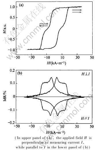
Fig.1 Normalized hysteresis loop(a) and MR curves(b) for Si(100)/Cr 5nm/Co 5nm/Si 2.7nm/Co 5nm
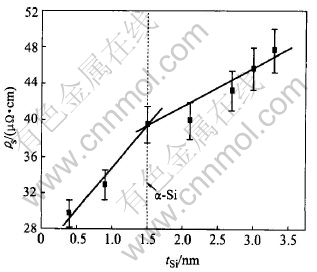
Fig.2 Saturation resistivity ��s dependence of sandwiches Si(100)/Cr 5nm/Co 5nm/Si tSi/Co 5nm on nominal Si thickness tSi
It is well known that evaporated Si are readily in an amorphous form, and the interdiffusion easily happens to form silicides at metal/��-Si interface[5-14, 16, 17]. It is also true in our case of Co/Si interface. Fig.2 shows the saturation resistivity dependence of the Co/Si/Co sandwiches on the nominal Si spacer thickness. In Fig.2, it is easy to find that the resistivity increases in two different rates before and after 1.5nm Si spacer thickness, which implies that the Co-Si interdiffusion occurs up to nominal 1.5nm Si and ��-Si appears in the Si spacer thicker than 1.5nm. The interdiffusion length of 1.5nm for Co/Si interface is consistent with results for other metal/��-Si interfaces[5, 6, 16, 17]. The further investigation revealed that the interface reaction at Co/Si is not asymmetric, i.e. the diffusion length of Co atoms into Si is larger than that of Si atoms into Co. The more detailed results on the Co/Si interdiffusion will be published elsewhere.
To overcome the drawback of highly resistive Si spacer, it is necessary to enhance the spin polarization of conduction electrons so that even after the spacer��s strong scattering, the highly spin-polarized conduction electrons can still reserve some spin information. Then, it��s possible to observe a GMR or spin-valve MR through the Si spacer. To do it, we replaced the top Co layer in the above mentioned Si(100)/Cr/Co/Si/Co structures with another Co/Cu/Co sandwich. It��s also well known that Co/Cu multilayers or Co/Cu/Co sandwiches have a high GMR effect[18] which, however, is mainly contributed to spin-dependent scattering at Co/Cu interface rather than that in bulk Co[19, 20]. It is conceivable that the top Co/Cu/Co sandwich will polarize conduction electrons more than only a single Co layer for its GMR mechanism and high spin-dependent scattering at Co/Cu interface. Furthermore, due to the strong interlayer coupling in Co/Cu/Co sandwich, the two Co layers show the same hysteresis loop(see Fig.3). So we can treat the top Co/Cu/Co sandwich as one single ferromagnetic layer. Fig.4 shows the MR curve and hysteresis loop for the structure of Si(100)/Cr 5nm/Co 5nm/Si 2.7nm/(Co 5nm/Cu 3nm/Co 5nm). At the thickness of 2.7nm, the Si spacer contains ��-Si besides the Co-Si silicide interface layers. Due to the decoupling effect of Si spacer, the hysteresis loop in Fig.4(b) has also two plateaus similar to those in Fig.1(a). On the plateaus, the magnetic moments of the bottom Co layer and the top Co/Cu/Co sandwich align themselves in opposite direction. To see the MR and hysteresis behavior of the top sandwich, we prepared a sandwich of Si(100)/Si 2.7nm/Co 5nm/Cu 3nm/Co 5nm and measured its MR curve and hysteresis loop which are also shown in Fig.4. An apparent difference between the MR curve of the sample Si(100)/Cr/Co/Cu/(Co/Cu/Co) and that of the sample Si(100)/Si/Co/Cu/Co is that on the root of declining edges, the former is convex while the latter is concave, see Figs.3 and 4. Furthermore, it is found that the convex parts on the MR curve are also located in the same applied field range of the plateaus on hysteresis loop for the sample Si(100)/Cr/Co/Cu/(Co/Cu/Co). So it can be considered that the MR on the convex curve is a result of anti-parallel alignment of the magnetic moments of the bottom Co layer and the top Co/Cu/Co sandwich. When we changed the angle between field H and current I, we found nearly no variance of the MR behavior and the convex shape remained, which indicates that the convex MR is not the characteristic of Co bulk, but a spin-valve MR through the ��-Si spacer. We took the MR of 0.5% at the edges of the plateaus on the hysteresis loop, about ��11.1kA/m, as the value of the spin-valve MR through the ��-Si spacer. At ��11.1kA/m, the top Co/Cu/Co sandwich should already be in the opposite magnetic saturation and has no spin-valve MR, while the bottom Co layer still remains its original magnetization orientation(see Fig.4).
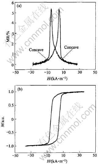
Fig.3 MR curve(a) and normalized hysteresis loop(b) for Si(100)/Cr 5nm/Co 5nm/Cu 3nm/Cu 5nm
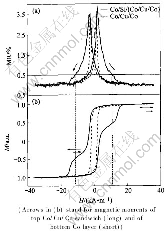
Fig.4 MR curves(a) and normalized hysteresis loops(b) for Si(100)/Cr 5nm/Co 5nm/Si 2.7nm/(Co 5nm/Cu 3nm/Co 5nm)
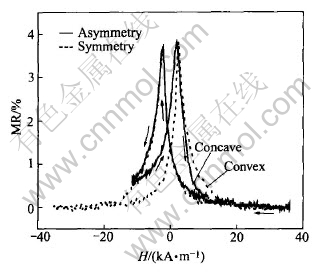
Fig.5 MR curves in symmetric field scan (dot line) and asymmetric field scan (solid line) for Si(100)/Cr 5nm/Co 5nm/Si 2.7nm/(Co 5nm/Cu 3nm/Co 5nm)
To prove the spin-valve MR through ��-Si spacer, we performed a MR measurement in an asymmetric scanning field. First, we put the sample Si(100)/Cr/Co/Cu/(Co/Cu/Co) in positive saturation field of 35.8kA/m to align both moments of bottom Co layer and top Co/Cu/Co sandwich. Then the field was reduced to zero and increased in reverse direction up to -11.5kA/m, after which the field was turned back to positive 11.5kA/m. The MR curve in such an asymmetric scan is shown in Fig.5(solid line), accompanied by the MR curve in full symmetric scan(dot line). It can be seen that the asymmetric MR from 35.8kA/m to -11.5kA/m follows the same trace as the symmetric MR. However, when coming back from -11.5kA/m, the asymmetric MR has a different behavior from the symmetric MR that the asymmetric MR curve is concave rather convex on the root of declining edge, as indicated in Fig.5. In the asymmetric scan, the magnetic moment of the bottom Co layer basically reserves its direction while the top Co/Cu/Co sandwich finishes a complete hysteresis loop. So the asymmetric MR is mainly the contribution of the top sandwich. Especially after the MR peak in the back scan of field from -11.5kA/m to 11.5kA/m, the magnetic moment of the top sandwich is reversed to be parallel again to that of the bottom Co layer, which eliminates the spin-valve MR between the two moments through the ��-Si spacer. So only the concave characteristic of top Co/Cu/Co sandwich appears on the asymmetric MR curve.
4 CONCLUSIONS
The electron-beam evaporated Co/Si/Co sandwiches show no indication of GMR or spin-valve MR. When the nominal thickness of Si spacer reaches 0.9nm, the interlayer coupling between the two Co layers is sufficiently reduced. The inter-diffusion length at Co/Si interface is about 1.5nm, above which amorphous Si(��-Si) forms. The high resistivity of Si spacer destroys the Co/Si/Co sandwiches�� GMR or spin-valve MR. By replacing the top Co layer in the Si(100)/Cr/Co/Si/Co structure with a top Co/Cu/Co sandwich, we have succeeded in observing a spin-valve MR of about 0.5% through an ��-Si spacer at room temperature. The GMR mechanism and high spin-dependent scattering at Co/Cu interface in top Co/Cu/Co sandwich enhance the spin polarization of conduction electrons, which in turn increases the spin-valve MR through an ��-Si spacer to an observable level.
REFERENCES
[1]Dieny B. Giant magnetoresistance in spin-valve multilayers [J]. J Magn Magn Mater, 1994, 136(3): 335-359.
[2]Wang D, Daughton J M, Smith C H, et al. Effect of Au underlayers on GMR properties of NiFe/Cu/CoFe sandwiches [J]. IEEE Transactions on Magnetics, 1996, 32(5): 4728-4730.
[3]Qian Z H, Daughton J M, Wang D X, et al. Magnetic design and fabrication of linear spin-valve sensors [J]. IEEE Transactions on Magnetics, 2003, 39(5): 3322-3324.
[4]Liu Y, Deac A, Li M, et al. Spin transfer effect in spin-valve pillars for current-perpendicular-to-plane magnetoresistive heads [J]. Journal of Applied Physics, 2004, 95(11): 7423-7428.
[5]Toscano S, Briner B, Hopster H, et al. Exchange-coupling between ferromagnets through a non-metallic amorphous spacer-layer [J]. J Magn Magn Mater, 1992, 114: L6-L10.
[6]Fullerton E E, Mattson J E, Lee S R, et al. Magnetic decoupling in sputtered Fe/Si superlattices and multilayers [J]. J Appl Phys, 1993, 73: 6335-6337.
[7]Mattson J E, Kumar S, Fullerton E E, et al. Photo-induced antiferromagnetic interlayer coupling in Fe/(Fe-Si) superlattices [J]. Phys Rev Lett, 1993, 71: 185-188.
[8]Briner B, Landolt M. Intrinsic and heat-induced exchange coupling through amorphous silicon [J]. Phys Rev Lett, 1994, 73: 340-343.
[9]Fullerton E E, Bader S D. Temperature-dependent biquadratic coupling in antiferromagnetically coupled Fe/FeSi multilayers [J]. Phys Rev B, 1996, 53: 5112-5115.
[10]Lai H H, Chen W C, Yao Y D. Effects of orientation and temperature on magnetoresistance of Fe/Si multilayers [J]. J Magn Magn Mater, 2004, 282: 96-99.
[11]Vries J J, Kohlhepp J, Broeder F J A, et al. Exponential dependence of the interlayer exchange coupling on the spacer thickness in MBE-grown Fe/SiFe/Fe sandwiches [J]. Phys Rev Lett, 1997, 78: 3023-3026.
[12]Inomata K, Yusu K, Saito Y. Magnetoresistance associated with antiferromagnetic interlayer coupling spaced by a semiconductor in Fe /Si multilayers [J]. Phys Rev Lett, 1995, 74: 1863-1866.
[13]Broeder F J A, Kohlhepp J. Comment on ��magnetoresistance associated with antiferromagnetic interlayer coupling spaced by a semiconductor in Fe/Si multilayers�� [J]. Phys Rev Lett, 1995, 75: 3026-3026.
[14]Endo Y, Kitakami O, Shimada Y. Measurement of perpendicular giant magnetoresistance of Fe/Si superlattices [J]. Appl Phys Lett, 1998, 72: 495-497.
[15]Chen G. New longitudinal recording media CoxNiyCrz for high rate static magnetron sputtering system [J]. IEEE Trans Magn, 1986, 22: 334-336.
[16]Dufour C, Bruson A, George B. Polarized neutron study of Fe/Si multilayers [J]. Solid State Communication, 1989, 69: 963-968.
[17]Stearns M B, Chang C H, Stearns D G. Optimization of growth conditions of vapor deposited Mo/Si multilayers [J]. J Appl Phys, 1992, 71: 187-195.
[18]Parkin S S P, Bhadra R, Roche K P. Oscillatory magnetic exchange coupling through thin copper layers [J]. Phys Rev Lett, 1991, 66: 2152-2155.
[19]Parkin S S P. Origin of enhanced magnetoresistance of magnetic multilayers: Spin-dependent scattering from magnetic interface states [J]. Phys Rev Lett, 1993, 71: 1641-1644.
[20]Lenczowski S K J, Gijs M A M, Giesbers J B, et al. Interpretation of the giant magnetoresistance effect in Co/Cu(100) multilayers with the quantum model of giant magnetoresistance [J]. Phys Rev B, 1994, 50: 9982-9988.
(Edited by YUAN Sai-qian)
Received date: 2005-05-08; Accepted date: 2005-10-19
Correspondence: SHEN Hong-lie, Professor, PhD; Tel: +86-25-84896270; E-mail: hlshen@nuaa.edu.cn