Trans. Nonferrous Met. Soc. China 24(2014) 3181-3188
Effect of deposition parameters on micro- and nano-crystalline diamond films growth on WC-Co substrates by HFCVD
Jian-guo ZHANG, Xin-chang WANG, Bin SHEN, Fang-hong SUN
School of Mechanical Engineering, Shanghai Jiao Tong University, Shanghai 200240, China
Received 30 October 2013; accepted 10 February 2014
Abstract: The characteristics of hot filament chemical vapor deposition (HFCVD) diamond films are significantly influenced by the deposition parameters, such as the substrate temperature, total pressure and carbon concentration. Orthogonal experiments were introduced to study the comprehensive effects of such three parameters on diamond films deposited on WC-Co substrates. Field emission scanning electron microscopy, atomic force microscopy and Raman spectrum were employed to analyze the morphology, growth rate and composition of as-deposited diamond films. The morphology varies from pyramidal to cluster features with temperature decreasing. It is found that the low total pressure is suitable for nano-crystalline diamond films growth. Moreover, the substrate temperature and total pressure have combined influence on the growth rate of the diamond films.
Key words: hot filament chemical vapor deposition (HFCVD); diamond films; WC-Co substrates; deposition parameters
1 Introduction
Diamond films have received intensively investigations as protecting coatings due to their attractive properties such as high hardness, good wear resistant, low friction coefficient and favorable chemical inertness [1-3]. Hot filament chemical vapor deposition (HFCVD) method is widely used for depositing diamond films because of its geometry simplicity and comparative low cost. The parameters, such as substrate temperature (t), total pressure (p) and carbon content (x), are the main parameters that govern the growth process and the quality of as-deposited diamond films [4]. Some investigations on the effects of the parameters on CVD diamond films growth have been reported in available literatures.
ALI and  [5] investigated the effect of a wide range of methane concentrations from 0.5% to 3.5% (volume fraction) on surface morphology, growth rate and quality of diamond films. They concluded that with an increasing CH4 volume fraction, the diamond cluster decreased but the growth rate increased. Besides, the favorable polycrystalline orient (220) could be obtained at 2.5% and 3.0% CH4. The effects of CH4 concentration on diamond films grown on Si substrates were also studied by other researchers; they revealed that the non-diamond carbon and growth rate are enhanced by increasing the CH4 concentration [6,7]. Besides, TAHER et al [8] compared physical properties of diamond coatings on WC-Co tool inserts with different CH4 concentrations and achieved the optimal parameters with CH4 concentration ranging from 1% to 3%. FABISIAK et al [9] studied the effect of the total gas pressure in the range of 2.0-12.0 kPa on diamond films growth on silicon wafers, showing that well-defined (100) crystal planes indicating high-quality diamond films are obtained at 8 kPa. YU and
  [10] also studied the effect of pressure on surface morphologies and crystal orientations of diamond films, demonstrating that the low pressure (650 Pa) was favorable for (111) facets growth and high pressure (2.6 kPa) was beneficial of (100) facets growth. KOBAYASHI et al [11] synthesized different diamond films with the pressure varying from 5 to 160 kPa (atmospheric pressure). The results indicated that the higher quality and growth rate of diamond films were obtained at atmospheric pressure. WEI et al [12] studied the effect of temperature on nano-crystalline diamond films on WC-13% Co (mass fraction) substrates and found that higher temperature is in favor of promoting the diamond nucleation and improving the adhesive strength between diamond films and substrates. Moreover, they also studied the effect of the filament-substrate separation on diamond growth on WC-Co bar substrates, proving that the growth rate, film quality and surface morphology are all sensitive to the filament-substrate separation [13]. Besides, the incorporation of dopants, such as oxygen, nitrogen and argon, also affects the characterization of as-fabricated CVD diamond films [14-18].
What’s more, deposition parameters are interdependent on the characterization of as-deposited diamond films. SALGUEIREDO et al [19] adopted a Taguchi matrix to design the experiments, with the purpose of studying the comprehensive effects of several key deposition parameters on diamond films growth on SiC substrates, including the gas composition, total gas pressure, total mass flow and substrate temperature. HUNG and SHIH [20] studied the effects of various control factors on the performance of microwave plasma enhanced CVD (MPECVD) diamond films, concluding that the bias voltage, methane concentration and hydrogen flow rate are the most important influencing factors on the quality of MPECVD diamond films. MALLIKA and KOMANDURI [21] investigated the effects of the chamber pressure, substrate temperature, microwave power and CH4 concentration on diamond films growth on silicon nitride cutting tools and found the optimum deposition conditions for producing high-quality diamond coatings. However, most of the researchers focused on the diamond films grown on the Si-related substrates. Moreover, the combined effects of the total pressure, substrate temperature and carbon content on diamond deposition on WC-Co substrates are rarely investigated.
In the present work, in order to investigate the mutual effects of the parameters on diamond films deposition on WC-Co substrates, the orthogonal experiment method is adopted. The effects of various deposition parameters on the surface morphology, growth rate and chemical structure of as-deposited diamond films are studied with the field emission scanning electron microscope (FE-SEM), atomic force microscope (AFM) and Raman spectrum. Furthermore, the adhesive strength between the film and substrate is also evaluated by Rockwell indentation tests. The results of this study are expected to provide helpful guidance for fabricating high-quality diamond coated WC-Co tools with complex geometries.
2 Experimental
The WC-6%Co inserts with dimensions of 13 mm×13 mm×4 mm were used as the substrates. Prior to the deposition process, the WC-Co inserts were pretreated by a two-step chemical etching method. Firstly, the WC-Co inserts were dipped in the Murakami’s reagent of 10 g K3Fe(CN)6 + 10 g KOH + 100 mL H2O in an ultrasonic vessel for 30 min. The second etching step was performed using acid solution of 20 mL HCl + 80 mL H2O2 to etch the cobalt on the surfaces. Subsequently, the inserts were ground with 5 μm diamond powders and then cleaned ultrasonically with acetone for 5 min. Tantalum wires (d0.5 mm) were used as hot filaments, which were dragged to be straight and fixed above the substrates, as shown in Fig. 1. In order to obtain uniform substrate temperature distribution, the filaments were arranged in parallel and equidistance manner displayed in Fig. 1(b), in which the filament- substrate separation (H) was defined as the distance between the top of substrate and the horizontal plane of filaments. During the deposition process, the substrate temperature was changed by adjusting H. A temperature measuring system was adopted to monitor the substrate temperature during the deposition process. During the deposition process, when the filament power reached (2000±5) W, the average temperatures were 930, 810 and 650 °C according to H=5, 10 and 15 mm, respectively.
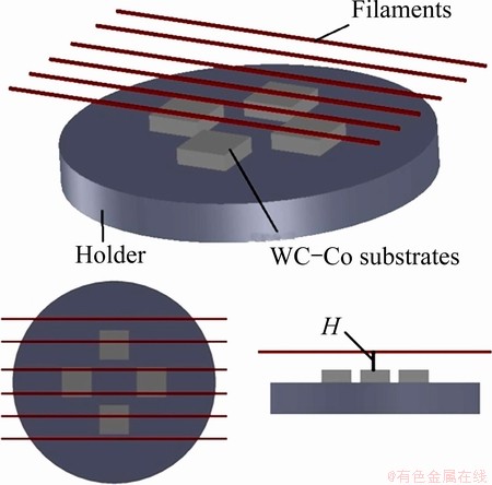
Fig. 1 Schematic diagram of filament-substrate system
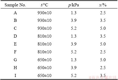
The deposition experiments were developed from the theory of orthogonal design to study three variables at three levels each based on the Taguchi method [22]. The three chosen variables were: substrate temperature, total pressure and carbon content (the volume ratio of acetone gas to hydrogen). This design permitted the determination of the relative importance of each variable on the diamond films’ characteristics. In this study, such the three variables were identified and observed in an L(3×3) orthogonal array experiment with three levels, as shown in Table 1.
As-fabricated diamond films with different parameters were characterized with the field emission scanning electron microscope (FE-SEM, Zeiss ULTRA55), atomic force microscope (AFM, NanoScope IIIa) and Raman spectroscope (SPEX1403) equipped with He-Ne laser (λ=632.8 nm). Moreover, the Rockwell indentation tests were conducted to assess the adhesive strength between the diamond film and substrate with a load of 980 N at the diamond indenter.
Table 1 Experimental layout using L(3×3) orthogonal array
3 Results and discussion
3.1 Surface morphology
The surface morphologies of diamond films deposited under different conditions are shown in Fig. 2. The surface morphology of the diamond films in the present study is mainly defined as the grain size, which can be distinguished into three levels: micro-crystalline, sub-microcrystalline and nano-crystalline. The ball-like morphologies with structures made up of nano- crystalline grains are presented in Figs. 2(a) and (d) under the conditions of p=1.3 kPa, t=930 °C and p=1.3 kPa, t=810 °C. On the contrary, pyramidal features of the diamond particles are observed in Figs. 2(b), (c) and (e)-(g). Besides, the grain sizes of the diamond films deposited at higher temperatures (Figs. 2(b) and (c)) are significantly larger than those at lower temperatures (Figs. 2(e)-(g)). Figures 2(b) and (c) show the dense and homogeneous well-faceted polycrystalline diamond films with particle size of ~1.5 μm at 930 °C. In Fig. 2(e), the surface morphology becomes discontinuous at 810 °C and the large clusters made up of fine grains are obvious. However, the surface of the sample F (Fig. 2(f)) is also dense, due to the high total pressure (5.2 kPa). It is noted that the diamond films in Fig. 2(g) display pyramid-like structures but not ball-like morphologies, which are different from samples A and D at the same total pressure, possibly due to the comprehensive effects of the high carbon content (5%, volume fraction) and lower substrate temperature. Moreover, the agglomerations of diamond films with sub- microcrystalline particles are observed from Figs. 2(h) and (i). The surface morphology is determined by the appearance of crystal facets and crystallographic orientation, which is expressed by the α parameter [23]. The α parameter mainly depends on the deposition parameters [24]. The domains of (100) and (111) oriented growth of diamond films of all the samples (except samples A and D) are grown at the condition of α>3 [25,26]. For samples A and D, the ball-like structures are attributed to the non-diamond phases nucleating on both (111) and (100) faces under the condition of 2<α<3 [27].
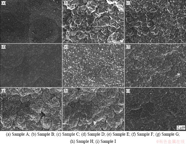
Fig. 2 SEM images of samples
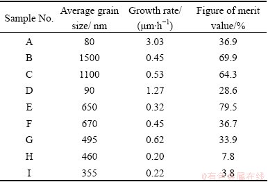
The corresponding AFM images of as-deposited diamond films are shown in Fig. 3. In order to identify the grain size of different diamond films, the scanning area for nano-crystalline diamond films (Figs. 3(a) and 3(d)) is 0.5 μm×0.5 μm, and that for the others is 10 μm×10 μm. The average grain sizes of all the samples are listed in Table 2. Overall, the diamond films deposited at 930 °C and 810 °C present well-faceted pyramidal features, while the film deposited at 650 °C shows cluster shapes consisting of fine grains. It is noted that there are many valley areas between the clusters, indicating the poor density of the surfaces. The results suggest that the total pressure has the most notable effect on the grain size, followed by the substrate temperature.
3.2 Growth rate
In order to investigate the growth rate, the samples are cut off by electric discharge machining. The film thickness is measured according to the cross-sectional morphologies, as shown in Fig. 4. The approximate growth rates are listed in Table 2, which range from ~0.2 to ~3.03 μm/h. At the pressure of 1.3 kPa, a relatively high growth rate is obtained with the higher substrate temperature. The nano-crystalline diamond films display the continuous growth of nanostructure diamond, as shown in Figs. 4(a) and (d). Furthermore, in the cases of 3.9 kPa and 5.2 kPa, the growth rate increases with the increment of substrate temperature and carbon content. It can be concluded that the total pressure has the most significant impact on the growth rate.
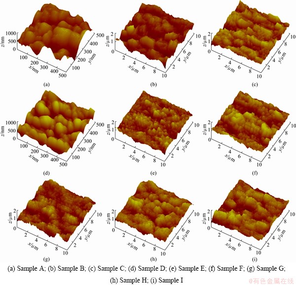
Fig. 3 AFM image of samples
Table 2 Average grain sizes, growth rate and figure of merit value
3.3 Raman spectroscopy analysis
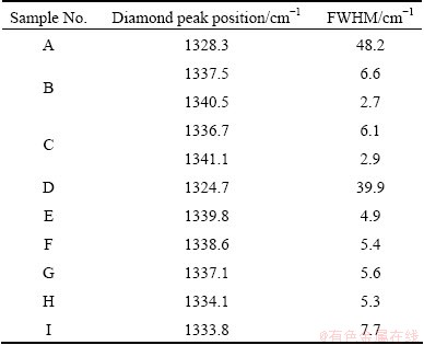
Raman spectroscopy is frequently used to characterize the CVD diamond films, giving the ability of being sensitive to the different carbon phases [28]. The Raman spectra of the diamond films deposited with different parameters are plotted in Fig. 5. In order to assess the effects of the deposition variables, the Raman spectra are all deconvoluted and analyzed by multi- Gaussian peak fitting. The diamond peak positions and FWHMs (full width at half maximum) observed for all samples are given in Table 3. The nano-crystalline diamond features are exhibited in Figs. 5(a) and (d), in which the diamond position peaks are respectively at 1328.3 cm-1 and 1324.7 cm-1. In Fig. 5(a), the presence of a broad feature at ~1250 cm-1 is ascribed to the amorphous sp3-bonded carbon [29,30]. The bands at 1490.6 cm-1 and 1592.1 cm-1 are corresponding to the trans-polyacetylene and graphite (sp2) structure [31,32]. For sample B, the typical sp3 diamond peak shifts from its normal position at 1332 cm-1 and splits into two components (doublet phonon at higher frequency of 1340.5 cm-1 and singlet phonon at lower frequency of 1337.5 cm-1), which is resulted from the large compressive residual stress presented in the films [33]. The Raman spectrum of sample C is similar to that of sample B, with two bands at 1336.7 cm-1 and 1341.1 cm-1 for diamond peaks, indicating that the higher substrate temperature will lead to higher residual stresses. From Figs. 5(e) to (i), it can be observed that the non-diamond phases increase as the temperature decreases. The figure of merit value (Q) for the amount of diamond in the deposition is calculated by the ratio of ID/(ID+IC), where ID is the integrated intensity of diamond peak and IC is the integrated intensity of the non-diamond carbon [34]. It can be noticed that the most notable influencing factor on the structural quality of the diamond films is the substrate temperature, manifesting that the higher t will lead to higher Q, suggesting the better quality.
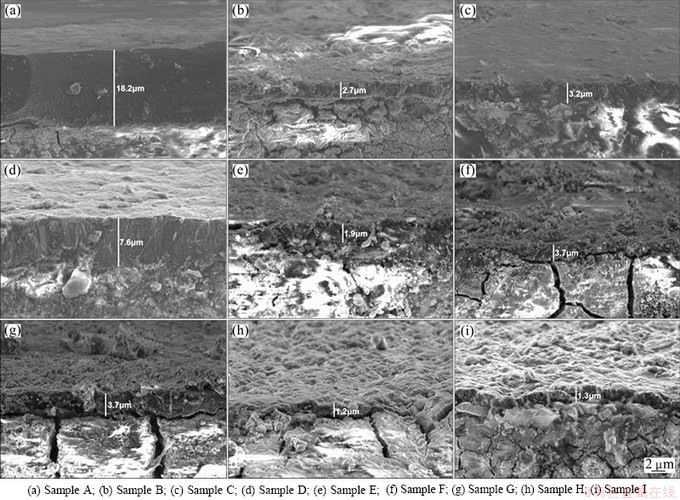
Fig. 4 SEM images of fracture cross-section of samples
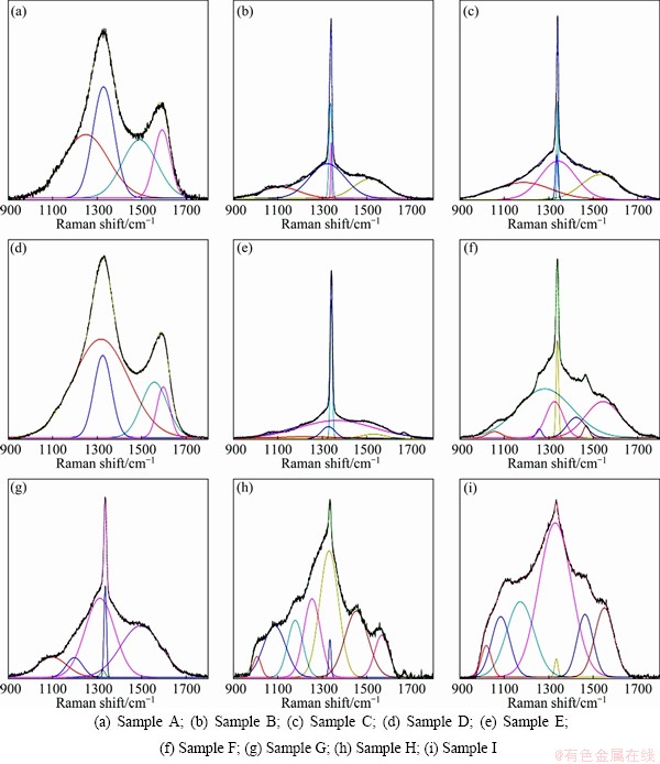
Fig. 5 Raman spectra of diamond films of samples
Table 3 Peak position and FWHM of diamond
3.4 Adhesive strength
The SEM images of the indentations on the different samples are shown in Fig. 6. At 930 °C, flaking off of the films is obvious, as demonstrated in Figs. 6(a)-(c). The peeling area on sample C is larger than that on sample A. For sample B, there are many long cracks around the indentation imprint, which are attributed to the higher residual stress in the films induced by the higher temperature. With temperature decreasing from 810 to 650 °C, the peeling area becomes smaller. Besides, the adhesive strength is also associated with the film thickness. The samples deposited at 650 °C display good adhesion, mainly due to the small thickness. As to the nano-diamond films in Figs. 6(a) and (d), severer delamination occurs on the nano-crystalline films with the thickness of 7.6 μm, indicating that increasing film thickness will generally increase the resistance of film delamination [35].
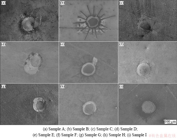
Fig. 6 SEM images of Rockwell indentations on diamond films of samples
4 Conclusions
1) The three-factor, three-level fractional factorial design experiments are conducted to investigate the effects of several key deposition parameters on the diamond films grown on WC-Co substrates by HFCVD method.
2) The substrate temperature is found to have notable effects on the diamond structural quality. The total pressure has the greatest impact on the grain size and growth rate while has the minimum influence on the structural quality.
3) In the range of carbon content used in this investigation, the carbon content has no significant effect on the grain size and growth rate. The lower total pressure (1.3 kPa) is beneficial to fabricating nano-diamond films. This study can be extended to fabricate high-quality diamond coated WC-Co tools with complex geometries.
References
[1] SHEN Bin, SUN FANG-hong. Deposition and friction properties of ultra-smooth composite diamond films on Co-cemented tungsten carbide substrates [J]. Diamond and Related Materials, 2009, 18(2-3): 238-243.
[2] AHMED W, SEIN H, JACKSON M, POLINI R. Chemical vapour deposition of diamond films onto tungsten carbide dental burs [J]. Tribology International, 2004, 37(11-12): 957-964.
[3] CHEN Su-lin, SHEN Bin, ZHANG Jian-guo, WANG Liang, SUN Fang-hong. Evaluation on residual stresses of silicon-doped CVD diamond films using X-ray diffraction and Raman spectroscopy [J]. Transactions of Nonferrous Metals Society of China, 2012, 22: 3021-3026.
[4] RAMOS S C, AZEVEDO A F, BALDAN M R, FERREIRA N G. Effect of methane addition on ultrananocrystalline diamond formation: Morphology changes and induced stress [J]. Journal of Vacuum Science and Technology A, 2010, 28: 27-32.
[5] ALI M,  M. Surface morphology, growth rate and quality of diamond films synthesized in hot filament CVD system under various methane concentrations [J]. Applied Surface Science, 2011, 257(20): 8420-8426.
[6] SCHIRACH R J, KOLBESEN B O, ADERHOLD D D, COMES F J. Characterization of crystal faces of polycrystalline HFCVD diamond films by STM/STS [J]. Fresenius' Journal of Analytical Chemistry, 1997, 358(1-2): 335-338.
[7] MENON P M, CLAUSING R E, HEATHERLY L, FEIGERLE C S. The morphology of diamond grown by hot filament chemical vapor deposition [J]. Diamond and Related Materials, 1998, 7(8): 1201-1206.
[8] TAHER M A, SCHMIDT W F, NASEEM, BROWN W D, MALSHE A P, NASRAZADANI S. Effect of methane concentration on physical properties of diamond-coated cemented carbide tool inserts obtained by hot-filament chemical vapour deposition [J]. Journal of Materials Science, 1998, 33(1): 173-182.
[9] FABISIAK K, BANASZAK A, KACZMARSKI M, KOZANECKI M. Structural characterization of CVD diamond films using Raman and ESR spectroscopy methods [J]. Optical Materials, 2006, 28(1-2): 106-110.
[10] YU Z,  A. Pressure dependence of growth mode of HFCVD diamond [J]. Diamond and Related Materials, 1997, 6(1): 81-84.
[11] KOBAYASHI T, HIRAKURI K K, MUTSUKURA N, MACHI Y. Synthesis of CVD diamond at atmospheric pressure using the hot-filament CVD method [J]. Diamond and Related Materials, 1999, 8(6): 1057-1060.
[12] WEI Q P, YU Z M, MA L, YIN D F, YE J. The effects of temperature on nanocrystalline diamond films deposited on WC-13%Co substrate with W-C gradient layer [J]. Applied Surface Science, 2009, 256(5): 1322-1328.
[13] WEI Q P, ASHFOLD M N R, MANKELEVICH Y A, YU Z M, LIU P Z, MA L. Diamond growth on WC-Co substrates by hot filament chemical vapor deposition: Effect of filament–substrate separation [J]. Diamond and Related Materials, 2011, 20(5-6): 641-650.
[14] WANG Lin, WANG Yong-ming, ZHOU Jian, OUYANG Shi-xi. Diamond films produced by microwave plasma chemical vapor deposition at low temperature and their characterization [J]. Materials Science and Engineering A, 2008, 475(1-2): 17-19.
[15] TANG C J, ABE I, FERNANDES A J S, NETO M A, GU L P, PEREIRA S, YE H, JIANG X F, PINTO J L. A new regime for high rate growth of nanocrystalline diamond films using high power and CH4/H2/N2/O2 plasma [J]. Diamond and Related Materials, 2011, 20(3): 304-309.
[16] TANG C J, NEVES A J, PEREIRA S, FERNANDES A J S,  J, CARMO M C. Effect of nitrogen and oxygen addition on morphology and texture of diamond films (from polycrystalline to nanocrystalline) [J]. Diamond and Related Materials, 2008, 17(1): 72-78.
[17] TANG C J, ABE I, VIEIRA L G, SOARES M J,  J, PINTO J L. Investigation of nitrogen addition on hydrogen incorporation in CVD diamond films from polycrystalline to nanocrystalline [J]. Diamond and Related Materials, 2010, 19(5-6): 404-408.
[18] MA Y P, SUN F H, XUE H G, ZHANG Z M, CHEN M. Deposition and characterization of nanocrystalline diamond films on Co-cemented tungsten carbide inserts [J]. Diamond and Related Materials, 2007, 16(3): 481-485.
[19] SALGUEIREDO E, AMARAL M, NETO M A, FERNANDES A J S, OLIVEIRA F J, SILVA R F. HFCVD diamond deposition parameters optimized by a Taguchi matrix [J]. Vacuum, 2011, 85(6): 701-704.
[20] HUNG C C, SHIH H C. Experimental design method applied to microwave plasma enhanced chemical vapor deposition diamond films [J]. Journal of Crystal Growth, 2001, 233(4): 723-729.
[21] MALLIKA K, KOMANDURI R. Low pressure microwave plasma assisted chemical vapor deposition (MPCVD) of diamond coatings on silicon nitride cutting tools [J]. Thin Solid Films, 2001, 396(1-2): 146-166.
[22] GONG Guang-cai, XU Chun-wen, JIAO Jun-jun, LIU Yuan-kun, XIE Sai-nan. Investigation of moisture condensation on papermaking plant envelopes in high humidity environment by orthogonal analysis and CFD simulation [J]. Building and Environment, 2011, 46(8): 1639-1648.
[23] YOKOTA Y, ANDO Y, KOBASHI K, HIRAO T, OURA K. Morphology control of diamond films in the region of α=1-1.5 using a 60 kW microwave plasma CVD reactor [J]. Diamond and Related Materials, 2003, 12(3-7): 295-297.
[24] WILD C, KOIDL P,  W, WALCHER H, KOHL R, HERRES N, LOCHER R. Chemical vapour deposition and characterization of smooth {100}-faceted diamond films [J]. Diamond and Related Materials, 1993, 2(2-4): 158-168.
[25] KUMAGAI K, MIYATA K, NISHIMURA K, KABASHI K. Growth of (110)-oriented diamond films by electron-assisted chemical vapor deposition [J]. Journal of Materials Research, 1993, 8(2): 314-320.
[26] WILD C, KOHL R, HERRES N,  W, KOIDL P. Oriented CVD diamond films: twin formation, structure and morphology [J]. Diamond and Related Materials, 1994, 3(4-6): 373-381.
[27] GICQUEL A, HASSOUNI K, SILVA F, ACHARD J. CVD diamond films: From growth to applications [J]. Current Applied Physics, 2001, 1(6): 479-496.
[28] ASKARI S J, CHEN G C, AKHTAR F, LU F X. Adherent and low friction nano-crystalline diamond film grown on titanium using microwave CVD plasma [J]. Diamond and Related Materials, 2008, 17(3): 294-299.
[29] MILLS R, SANKAR J, VOIGT A, HE J, RAY P, DHANDAPANI B. Role of atomic hydrogen density and energy in low power chemical vapor deposition synthesis of diamond films [J]. Thin Solid Films, 2005, 478(1-2): 77-90.
[30] PRAWER S, NUGENT K W, JAMIESON D N, ORWA J O, BURSILL L A, PENG J L. The Raman spectrum of nanocrystalline diamond [J]. Chemical Physics Letters, 2000, 332(1-2): 93-97.
[31] FERRARI A C, ROBERTSON J. Origin of the 1150-cm-1 Raman mode in nanocrystalline diamond [J]. Physical Review B, 2001, 63: 121405(R).
[32] YANG T S, LAI J Y, CHENG C L, WONG M S. Growth of faceted, ballas-like and nanocrystalline diamond films deposited in CH4/H2/Ar MPCVD [J]. Diamond and Related Materials, 2001, 10(12): 2161-2166.
[33] AGER III J W, DRORY M D. Quantitative measurement of residual biaxial stress by Raman spectroscopy in diamond grown on a Ti alloy by chemical vapor deposition [J]. Physical Review B, 1993, 48: 2601-2607.
[34] SAILS S R, GARDINER D J, BOWDEN M, SAVAGE J, RODWAY D. Monitoring the quality of diamond films using Raman spectra excited at 514.5 nm and 633 nm [J]. Diamond and Related Materials, 1996, 5(6-8): 589-591.
[35] QIN F, CHOU Y K, NOLEN D, THOMPSON R G. Coating thickness effects on diamond coated cutting tools [J]. Surface and Coatings Technology, 2009, 204(6-7): 1056-1060.
沉积参数对硬质合金基体微/纳米金刚石薄膜生长的影响
张建国,王新昶,沈 彬,孙方宏
上海交通大学 机械与动力工程学院,上海 200240
摘 要:基体温度、反应压力和碳源浓度等沉积参数决定热丝化学气相沉积金刚石薄膜的性能。运用正交试验方法,研究参数对硬质合金基体金刚石薄膜生长的综合作用。采用场发射扫描电镜(FE-SEM)、原子力显微镜(AFM)和拉曼(Raman)光谱检测薄膜的形貌结构、生长速率和成分。结果表明:随着基体温度的降低,金刚石形貌从锥形结构向团簇状结构转变;低反应压力有利于纳米金刚石薄膜的生成;生长速率受反应压力和碳源浓度综合作用的影响。
关键词:热丝化学气相沉积;金刚石薄膜;WC-Co硬质合金基体;沉积参数
(Edited by Xiang-qun LI)
Foundation item: Project (2012ZX04003-031) supported by the National Science and Technology Major Project, China
Corresponding author: Fang-hong SUN; Tel: +86-21-34206557; Fax: +86-21-34206556; E-mail: sunfanghong@sjtu.edu.cn
DOI: 10.1016/S1003-6326(14)63458-0