
Effect of dipole layer of Alq3 and metal on organic electroluminescence
XU Xue-mei(许雪梅)1, WU Jian-hao(吴建好)1, WANG Hua(王 华)1, WU Cheng-de(吴承德)1,
YE Jun-hua(叶俊华)1, WU Ai-jun(吴爱军)1, QU Shu(瞿 述)2, PENG Jing-cui(彭景翠)2
1. School of Physics Science and Technology, Central South University, Changsha 410083, China;
2. School of Physics and Microelectronics Technology, Hunan University, Changsha 410082, China
Received 15 July 2007; accepted 10 September 2007
Abstract: The effect of dipole layer of Alq3 and metal on organic electroluminescence in organic light-emitting diodes (OLEDs) was discussed. The relations among energy level alignment, interface charge transfer and dipole layer formation were well analyzed. An interface dipole layer and charge transfer were observed by XPS and UPS. As for Alq3 with metallic film such as Al and Mg, N 1s, O 1s and C 1s all move to low binding energy. Both Alq3/Al and Alq3/Mg have different electron spectrum from that of simple Alq3 film. It is really the reason of the interface energy change that the metal atoms located near the interface move to organic layer and then chemically interact with O and C of Alq3. The injection voltage barrier heights of electrons at Alq3/Al and Alq3/Mg interface are 0.1 eV and 0.2 eV, respectively. Charge transfer lowers electrons injection voltage barrier height and forms good electrons injection interfaces. The width of dipole layer is about 5 nm. The knowledge of such interface dipole layer is essential for a proper understanding of the physical processes at the metal/organic interface.
Key words: interface dipole layer; organic electroluminescence; charge transfer; chemical reaction
1 Introduction
The metal/organic interface properties of organic light-emitting diodes (OLEDs) have been intensively investigated since the electroluminescence (EL) of 8-hydroxyquinoline aluminum (Alq3) was reported by TANG[1]. After an OLED is applied on voltage, charges move to organic materials near the interface. Part of charges, which are hindered by voltage barrier, will stay at the interface. These trap charges form dipole layer near the interface. The polarons, mirror image potential and electric field force near the interface will affect energy of electron, which makes Fermi level of metal drift and energy band of organic materials bend[2-4].
If dipole momentum points to organic layer, hole injection potential barrier  reduces and its injection ability rises, and verse visa. The dipole layer formed on surface by chemical adsorption or physical adsorption can heighten carriers injection ability. Many references reported that electron injection ability on the interface can be increased by proton injection or constructing molecule dipole layer[5-6]. Fig.1 shows that the formation of dipole layer has effect on the level array of metal/organic material interface, and the level bend of organic material is not considered. In Fig.1, EFA, EFC represent Fermi levels of the anode and cathode, respectively. If work function of metal or Fermi level changes, dipole layer will be formed on the interface. If molecule has higher dipole momentum, we can easily adjust the whole dipole layer by changing molecule dipole momentum by chemical ways.
Dipole layer has two contributions from the interface: one is the change of work function of metal, and the other is the charge transfer between metal and adsorbent[7-10]. Energy level array on the interface includes a serial of physical and chemical process, such as charge transfer, chemical reaction, and interface diffusion[11-14]. By molecule vibration spectrum, the dynamics phenomenon of charge transfer at the interface of Ag/organic and dipole modes of 1 563 cm-1 and 1 287 cm-1 were observed[10]. This describes the formation of dipole layer and energy level array, and finally affects the injection efficiency of electrons. The two tangible metal/organic interfaces are research in this work.
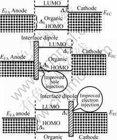
Fig.1 Interface formation of dipole layer and energy level array
2 Experimental
Indium-tin-oxide (ITO)-coated glass substrate was cleaned in ultrasonic baths of acetone and propanol for 1 h. Then they were introduced into the transferred ultraviolet (UV)-ozone cleaning chamber. After 30 min of UV-ozone treatment, hydrocarbons were effectively refilled with nitrogen, and the substrates were turned to the glove box. Alq3 was heated at 50 ℃ for 1 h and drop cast at a spin rate of 3 300 r/min. Typical film thickness was determined by an alpha-stepper. Then the cathodes (Al/Mg) were deposited through a shadow mask that defined two diodes per substrate with an active area of 25 mm2. And 60 nm Alq3 film, 80 nm Alq3/Al and 80 nm Alq3/Mg were obtained, while the thickness was monitored using a quartz crystal. The interface formation was studied by electron XPS gamma spectrum and UPS spectrum. XPS and UPS measurements were carried out under ultra high vacuum environment with base pressure less than 10-7 Pa. A un-monochromatized Mg Kα photon source with 1 486.6 eV photon energy was used for XPS and UPS measurements. The resolution of the spectrometer was set to 0.5 eV.
3 Results and discussion
3.1 Changes of structure of electrons at interface of Alq3/Al and Alq3/Mg
Fig.2 shows electron XPS gamma spectra of Al 2p, O 1s, C 1s and N 1s in clean Alq3, Alq3/Al and Alq3/Mg. The peak values of binding energy in clean Alq3 are 74.4, 531.5, 284.6 and 399 eV, respectively, which are in
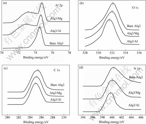
Fig.2 Electron XPS spectra of Al 2p(a), O 1s(b), C 1s(c) and N 1s(d) in Alq3, Alq3/Al and Alq3/Mg
good accordance with the results measured by NGUYEN. At the interface of Alq3/Al and Alq3/Mg, the location and shape of spectrum are changed. When metallic film was plated on the Alq3 film, it is shown that N 1s, O 1s and C 1s all move to low binding energy, which indicates there exists MOX at Alq3 near the interface. Besides, on the interface of Alq3/Al and Alq3/Mg, rump electron gamma spectrum appears another acromion at 72.6 eV and 72.8 eV, respectively. It is intensively shown that Al or Mg has spread in the organic layer. Alq3 has no peak values at 72.6 eV and 72.8 eV, that is to say, there is no simple substance of Al and Mg. So the appearance of acromion shows that the metal atoms located near the interface have penetrated into the organic layer and chemically reacted with O and C to produce complexes of metallic carbide or metal- oxygen-carbon, which shows a great deal of charge transfer at the interface.
3.2 Energy level distribution for interface dipole layer of Alq3/Al and Alq3/Mg
UPS measurement also indicates that there exists a great deal of charge transfer on the interface plated on the Alq3 film. It is shown that N 1s, O 1s and C 1s all move to low binding energy, which indicates there exists MOX at Alq3 near the interface. The change of electrons energy level Vb=1.1 eV, generally reflected the change of Alq3 energy level. The level of dipole layer Vdipole was decided by the gap between the change of work function of metal and the difference of electrons level. Suppose the change of work function of metal is  .
.  is the height of electron injection voltage barrier before the energy level drifts. ФAlq3 is the work function of Alq3. The height of electron injection voltage barrier becomes

 (1)
(1)
where Vdipole=-Vb. For Alq3/Al, Vdipole=0.2 eV; and for Alq3/Mg, Vdipole=0.4 eV. Electrons injection voltage barrier heights at two interfaces were =0.1 eV and 0.2 eV, respectively. Charge transfer lowered electrons injection voltage barrier height and formed good electrons injection interfaces. The width of dipole layer was about 5 nm. Fig.3 shows level array of Alq3/Al.
First, Al-N sigma bond formed at Alq3/metal, and then Al interacted with O until Alq3 ions formed. This intensively indicates that dipole layer was mainly restricted with organic molecule/metal interface. According to charge transfer and metal/organic material thermo-mechanics balance model, we could calculate the voltage barrier caused by dipole layer:
 (2)
(2)

Fig.3 Array of energy level of Alq3/Al
where Vdipole is negative relative to metal reference area, deff=min(a, dMs), a is effective distance of carrier jump in organic molecules, dMs is average distance between metal molecules and organic molecules, NB is chemical bond density led by chemical transform, ФM is work function of metal, χs is affinity of electrons, Eg is band gap of organic material, εIT is specific inductive capacity of interface area, k is the sum of coulomb reciprocity at the interface, F is electrical field strength, and e is fundamental electricity quantity of charge. When NB=0, there was no dipole layer. To some organic material, when NB and dMs are constant, Vdipole presented linear relation. On the other side, if Fermi level is close to some high density state, HOMO, LUMO or interface state may be approximately equal to affinity; while Fermi level was pinned at some high density state. Fermi level pinning at LUMO or HOMO in organic material is very important for device work, because it offers an injection interface for a zero voltage barrier. For materials that have low work function such as Ga, Mg and Na, the level analysis of XPS and UPS indeed indicates that Fermi level was pinned at Alq3 track. When the pinning phenomenon happens, relevant to Fermi level, organic materials level will not change any more. Any change of work function of metal will be made up by potential energy.
4 Conclusions
1) The injection barrier is not simply given by the difference of the electrode work function. As for Alq3 with metallic film such as Al and Mg, N 1s, O 1s and C 1s all move to low binding energy.
2) Both Alq3/Al and Alq3/Mg have different electron spectrum from that of simple Alq3 film. It is really the reason of the interface energy change that the metal atoms located near the interface move to organic layer and then chemically interact with O and C of Alq3.
3) Injection voltage barrier heights of electrons at Alq3/Al and Alq3/Mg interface are 0.1 eV and 0.2 eV, respectively. Charge transfer lowers electrons injection voltage barrier height and forms good electrons injection interfaces.
4) The width of dipole layer is about 5 nm. The change of chemical bond structure is another important factor deciding electrons characteristics near the interface, and the chemical reaction can largely change molecules characteristics.
References
[1] TANG C W, VANSLYKE S A, CHEN C H. Electroluminescence of doped organic thin films[J]. J Appl Phys, 1989, 65(9): 3610-3616.
[2] XU Xue-mei, PENG Jing-cui, QU Shu, LI Hong-jian, WU Jian-hao, OUYANG Yu. Recombination efficiency in double-layer organic light-emitting devices[J]. Chin Phys Lett, 2005, 22(3): 719-722.
[3] YAN L, GAO Y L. Interface in organic semiconductor devices[J]. Thin Solid Films, 2002, 417: 101-106.
[4] VAZQUEZ H, FLORES F, OSZWALDOWSKI R. Barrier formation at metal-organic interfaces: Dipole formation and the charge neutrality level[J]. Appl Surf Sci, 2004, 234: 107-112.
[5] HUANG Yong-hui, LI Hong-jian, DAI Guo-zhang, XIE Qiang, PAN Yan-zhi, DAI Xiao-yu. Performance enhancement by modification of cathode with a thin LiF layer in OLEDs[J]. Chin J Lumin, 2005, 26(6): 737-743. (in Chinese)
[6] CAO Y, PARKER I D, YU G. Improved quantum efficiency for electro-luminescence in semiconducting polymers[J]. Natrue, 1999, 397: 414-416.
[7] HOU Jing-ying, GAO Wen-bao, SUN Jia-xin. Improved efficiency of organic light-emitting diodes by doping each other between the organic layer[J]. Chin J Lumin, 2003, 24(2): 157-160. ( in Chinese)
[8] ZHAO Chu-jun, LI Hong-jian, HUANQ Bo-yun, CUI Hao-yang, XU Xue-mei. Influence of metal/organic interface barriers on the EL efficiency in single layer organic EL devices[J]. Chin J Lumin, 2004, 25(4): 401-406. (in Chinese)
[9] ZHANG S T, DING X M, ZHAO J M. Buffer-layer-induced barrier reduction: Role of tunneling in organic light-emitting devices[J]. Appl Phys Lett, 2004, 84(3): 425-427.
[10] KIM Y E, PARK H, KIM J J. Enhanced quantum efficiency in polymer electroluminescence devices by inserting a tunneling barrier formed by Langmuir-Blodgett films[J]. Appl Phys Lett, 1996, 69(5): 599-601.
[11] MORIT T, FUJIKAWA H, TOKITO S. Electronic structure of 8-hydroxyquinoline aluminum/LiF/Al interface for organic electroluminescent device studied by ultraviolet photoelectron spectroscopy[J]. Appl Phys Lett, 1998, 73(19): 2763-2765.
[12] ISHII H, SUGIYAMA K, ITO E. Energy level alignment and interfacial electronic structures at organic/metal and organic/organic interfaces[J]. Adv Mater, 1999, 11(8): 605-625.
[13] WANG X J, ZHAO J M, ZHOU Y C. Enhancement of electron injection in organic light-emitting devices using an Ag/LiF cathode[J]. J Appl Phys, 2004, 95 (7): 3828-3830.
[14] GROZEA D, TURAK A, FENG X D. Chemical structure of Al/LiF/Alq3 interfaces in organic light-emitting diodes[J]. Appl Phys Lett, 2002, 81(17): 3173-3175.
(Edited by YANG Bing)
Foundation item: Project(06JJ20034) supported by the Natural Science Foundation of Hunan Province, China; Project supported by the Theory Science Development Foundation of Central South University, China
Corresponding author: XU Xue-mei; Tel: +86-731-8836424; E-mail: xuxuemei999@126.com

