A reconfigurable computing architecture for 5G communication
��Դ�ڿ������ϴ�ѧѧ��(Ӣ�İ�)2019���12��
�������ߣ����� ���Ӿ� ���� � ������
����ҳ�룺3315 - 3327
Key words��5G communication; instruction set; register file; code compression; throughput; power consumption
Abstract: 5G baseband signal processing places greater real-time and reliability requirements on hardware. Based on the architecture of the MaPU, a reconfigurable computing architecture is proposed according to the characteristics of the 5G baseband signal processing. A dedicated instruction set for 5G baseband signal processing is proposed. The corresponding functional units are designed for reuse of hardware resources. A redirected register file is proposed to address latency and power consumption issues in internetwork. A two-dimensional code compression scheme is proposed for cases in which the use ratio of instruction memory is low. The access mode of the data memory is extended, the performance is improved and the power consumption is reduced. The throughput of 5G baseband processing algorithm is one to two orders of magnitude higher than that of the TMS320C6670 with less power consumption. The silicon area evaluated by layout is 5.8 mm2, which is 1/6 of the MaPU��s. The average power consumption is 0.7 W, which is 1/5 of the MaPU��s.
Cite this article as: GUO Yang, LIU Zi-Jun, YANG Lei, LI Huan, WANG Dong-lin. A reconfigurable computing architecture for 5G communication [J]. Journal of Central South University, 2019, 26(12): 3315-3327. DOI: https://doi.org/10.1007/s11771-019-4255-8.

J. Cent. South Univ. (2019) 26: 3315-3327
DOI: https://doi.org/10.1007/s11771-019-4255-8

GUO Yang(����)1, 2, LIU Zi-Jun(���Ӿ�)1, YANG Lei(����)1, LI Huan(�)1, WANG Dong-lin(������)1
1. Institute of Automation, Chinese Academy of Sciences, Beijing 100190, China;
2. University of Chinese Academy of Sciences, Beijing 100049, China
 Central South University Press and Springer-Verlag GmbH Germany, part of Springer Nature 2019
Abstract: 5G baseband signal processing places greater real-time and reliability requirements on hardware. Based on the architecture of the MaPU, a reconfigurable computing architecture is proposed according to the characteristics of the 5G baseband signal processing. A dedicated instruction set for 5G baseband signal processing is proposed. The corresponding functional units are designed for reuse of hardware resources. A redirected register file is proposed to address latency and power consumption issues in internetwork. A two-dimensional code compression scheme is proposed for cases in which the use ratio of instruction memory is low. The access mode of the data memory is extended, the performance is improved and the power consumption is reduced. The throughput of 5G baseband processing algorithm is one to two orders of magnitude higher than that of the TMS320C6670 with less power consumption. The silicon area evaluated by layout is 5.8 mm2, which is 1/6 of the MaPU��s. The average power consumption is 0.7 W, which is 1/5 of the MaPU��s.
Key words: 5G communication; instruction set; register file; code compression; throughput; power consumption
Cite this article as: GUO Yang, LIU Zi-Jun, YANG Lei, LI Huan, WANG Dong-lin. A reconfigurable computing architecture for 5G communication [J]. Journal of Central South University, 2019, 26(12): 3315-3327. DOI: https://doi.org/10.1007/s11771-019-4255-8.
1 Introduction
Wireless communication technology has evolved over four generations. It is evolving toward the fifth generation. The 5G communication system is expected to be mass-produced by 2020. 5G communication will have an ultra-high spectrum utilization and performance-to-power ratio. Its transmission rate and resource utilization will be an order of magnitude or greater than 4G. The user will experience communicate rate of over 1 Gbps. The end-to-end delay will be controlled in milliseconds. The flow density will reach tens of Tbps/km2. The connection density will reach 104/km2 [1, 2]. Such large amounts of data and high-speed transmission make greater demands on the performance and power consumption of the baseband processor. How to meet the high-throughput computing requirements with architecture that consumes less power has become a hot research topic.
Circuitry reconfiguration can dynamically change the function of the array of functional units (FUs) by configuring the stream at runtime [3]. Therefore, it is a calculation method driven by a configuration flow. The reconfigurable real-time circuits are similar to the instruction-driven processor in flexibility. In terms of energy efficiency, it could match the performance of application specific integrated circuit (ASIC). Most traditional baseband processors are ASIC, whose architecture is fixed and scalability is poor. Main communication equipment manufacturers have already begun to study programmable reconfigurable baseband processors [4].
WANG et al [5] introduced a novel architecture for data-intensive computing: mathematics processing unit (MaPU). It can configure the pipeline through microcode- controlled state machines to implement various algorithms. The core consists of three parts: a scalar pipeline, a microcode pipeline and a multi- granularity parallel memory, as shown in Figure 1. The scalar pipeline is composed of a scalar processing unit (SPU), which is responsible for scalar calculation, parameter configuration and external communication. The other is the microcode pipeline, which is composed of a microcode processing unit (MPU). It is responsible for intensive vector and matrix calculation. Its 512-bit single instruction multiple data (SIMD) architecture supports 64-byte, 32-half word and 16-word multi- granular operation. It also has a very long instruction word (VLIW) architecture with dozens of instruction slots for high parallelism. Multi- granular parallel memory supports the matrix row and column access of the three granularities. However, MaPU is still a large- scale matrix/vector computing architecture for general situations without targeted optimization for specific domains and specific algorithms. It is incompatible when applied to 5G communication scenarios. The incompatibility is reflected in the incomplete instruction set and micro-architecture design. Therefore, its performance is limited when faced with the baseband processing algorithms in the 5G communication field. Based on the computing architecture of MaPU, a computing architecture for the 5G communication field, universal communication processor (UCP) is proposed in this study. It can meet the high- throughput requirements of 5G baseband processing with low power consumption.
2 Related work
This section will introduce the architecture of several communication-specific DSPs. The hardware architecture of these products is deeply optimized for the algorithms of communication domain. But these processors are not optimized for the 5G standard. The architecture proposed in this paper is specifically optimized for the 5G NR standards which are proposed in 3GPP conference.
2.1 CEVA-XC12
Figure 2 shows the architecture of the XC12 launched by CEVA in February 2017 for future 5G communication [6]. Based on the XC4500, a communication-specific data processing unit and some new hard accelerators were added to the XC12. The above enhancements enable the XC12 to support multiple complex operations such as 256��256 multiple-input and multiple-output (MIMO), 1024 quadrature amplitude modulation (QAM) and 3D beamforming. The XC12 contains four vector processing units and one scalar processing units. Each vector processing unit supports 512-bit SIMD. It is VLIW architecture which includes multiple instruction slots (VA, VB,VM and VCU). It supports 16-bit fixed-point parallel multiplication of 128 MACs. Its coprocessor can efficiently implement discrete Fourier transformation (DFT), fast Fourier transform (FFT), Viterbi decoding and turbo decoding. In addition, the XC12 features FFT operations that support dynamic scaling and MAC with semi-complex features. Compared with the 4G-oriented CEVA-XC4500, the power consumption of CEVA-XC12 is reduced by half and the frequency can reach 1.8 GHz in the 10-nm process.
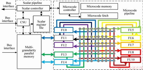
Figure 1 MaPU core architecture
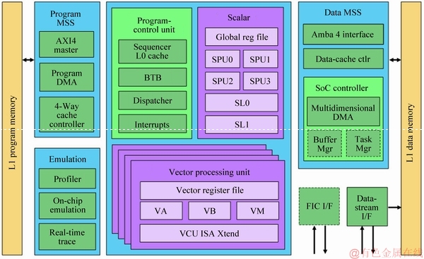
Figure 2 CEVA-XC12 architecture
2.2 TMS320C66x
C66x is a Texas Instruments (TI) multi-core processor series [7]. Figure 3(a) shows the architecture of the TMS320C6670 processor, which features a set of hard accelerators integrated as coprocessors, including FFTc for FFT/DFT, TCP3d for turbo decoding, BCP for receiver-side bit-level processing and TCP3e for transmitter-side bit-level processing. These accelerators greatly improve the processing speed of complex operations, which greatly improves the chip��s overall computing efficiency. However, the large number of hard accelerators makes the processor application scenario relatively simple. Its scalability and compatibility are poor. Figure 3(b) shows the core architecture of C66x. It includes two sets of arithmetic units, each of which includes a single- precision floating-point adder, a double-precision floating-point adder, a fixed-point adder and a multiplier. The processor supports 128-bit SIMD instructions. The frequency can reach 1.2 GHz in the 40-nm process.
2.3 Tensilica ConnX BBE64EP
The Cadence Tensilica ConnX BBE family [8] of enhanced performance digital signal processors (DSPs) establishes a new standard in high-performance, low-power digital signal processing specifically designed for high- performance baseband processing. Optimize complex number processing, the ConnX BBE DSPs offer significant improvements in maximum frequency and algorithmic performance while reducing both silicon area and power consumption versus earlier generations of DSPs.
The ConnX BBE64EP products are high- performance DSPs designed for next-generation communication systems. Advanced precision options are specifically designed to meet the precision and performance requirements associated with advanced MIMO systems. In addition to vector-based filtering, FFT and matrix capabilities, a fully featured instruction set includes a full range of bit-oriented operations.
The ConnX BBE64EP support 64-way multiplier-accumulator (MAC), dual 32-way arithmetic logic unit (ALU) SIMD. It has 5-issue VLIW for parallel load/store, MAC and ALU operations. Several optimized instructions is proposed: polynomial evaluation, block floating point, bit-oriented operations, vector compression and vector expansion. The memory bandwidth is 512 bits. There is a 32-bit scalar ALU.
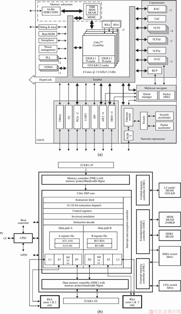
Figure 3 TMS320C6670 architecture (a) and C66x core (b)
3 5G instruction design
The instruction set architecture is directly related to an algorithmic execution efficiency in computing architecture. A set of instructions that are highly adaptable to the algorithm can bring the significant improvement in throughput. Some dedicated instructions for 5G baseband processing are proposed in this section.
The MaPU instruction set is a general-purpose matrix/vector operation calculation that supports general-purpose fixed-point, floating-point and logic operations. However, these general instructions will be incompatible when processing 5G baseband algorithms. Based on the advanced AppAISArcTM instruction set architecture proposed by WANG et al [5], the operators in the algorithm for the characteristics of 5G baseband processing is analyzed. Then, according to the MaPU architecture, the parallel implementation of the corresponding algorithm is designed. Based on the basic operations in the parallelization scheme, several dedicated instructions for 5G baseband processing are proposed in this section. According to these instructions, the architecture design of the corresponding functional unit (FU) is completed.
3.1 MAC design
MACs are the key components of the baseband processing. Convolution and filtering, which are often used in baseband processing, are performed by basic multiply-accumulate operations. MAC contains basic instructions related to multiplication and dedicated instructions for different operator acceleration. Based on the original MaPU instruction set, the following new instructions are proposed for 5G baseband processing.
3.1.1 Complex multiply, multiply-add, multiply-sub instruction
The data in the baseband processing usually exists in the form of a complex number. One complex multiplication includes four real multiplications and two real additions. Therefore, the compound instructions are proposed to accelerate complex multiplication. The MAC instructions are shown in Eq. (1). The symbol MAC represents the instruction that belongs to MAC. The symbols Ta and Tb represent the local registers in MAC. The options B and S represent the granularity of input data (8 bits, 16 bits and a default of 32 bits). These symbols are the same in the following text. Option H stands for conjugate multiplication. The default is regular complex multiplication. The Wallace tree of the UCP multiplier [9] is optimized. A 32��32-bit Booth encoder and Wallace tree can complete four 8��8-bits, two 16��16-bits and one 32��32-bit complex multiplication at a time.
 (1)
(1)
3.1.2 Complex multiply-accumulate instruction
Considering the data accuracy at the time of accumulation, the width of internal data is further increased on the basis of doubling, so as to prevent the accumulated result from overflowing. Therefore, for the multiply-accumulate operation of 8-bit, 16-bit and 32-bit data, the bit widths in the multiplier are 24, 40 and 72 bits respectively. Three complex multiply-accumulate instructions are shown in Eq. (2). The option CR in instruction 1 sets the Tc value to 0. Instruction 2 is the multiply-accumulate operation of the multiply- accumulate register (MR) and input data. The target fields of the first two instructions are the local MR. The accumulated result of instruction 3 is sent to the external register.
 (2)
(2)
3.1.3 FFT butterfly instruction
The above instructions are all general-purpose complex MAC instructions of MAC, which can be applied to most common operations. FFT butterfly operation is an important operator in baseband processing. The operation can be completed by a multiply-add and multiply-sub instruction. The MAC is added to the butterfly instruction to allow the butterfly operation to be completed by one instruction. Compared with the multiply-add, multiply-subtract operation, only two additions are added to the hardware resources. But its performance could be doubled. The FFT butterfly instruction is shown in Eq. (3).
 (3)
(3)
3.2 ALU design
The main functions of the ALU include basic arithmetic logic operations, comparison and selection operations. Based on the original MaPU instructions, the following new instructions are proposed for 5G baseband processing.
3.2.1 Add-modulo and sub-modulo instruction
For the cyclic shift operator of low density parity check (LDPC) encoding, the position of each byte before shifting is calculated according to the number of cyclic shifts. Because it is a cyclic shift, in the maximum range of the index, the original index value must be modulo the maximum range value after the addition or subtraction operation to obtain the rearranged address. Therefore, the add-modulo N instruction and the sub-modulo N instruction are added to the ALU as shown in Eq. (4). N is stored in Tc. The dedicated instruction can shorten three instructions into one.
 (4)
(4)
3.2.2 Merge-shift instruction
In polar encoding, the parallelization scheme of frozen bit insertion proposed by YANG et al [10] is to merge two vector vertical elements and then shift to the right. For this operation, the merge-shift instruction is added to the ALU, as shown in Eq. (5). The symbol imm represents the immediate operand. The dedicated instruction can shorten three instructions into one.
 (5)
(5)
3.2.3 Compare-select instruction
The horizontal update in LDPC decoding requires calculation of the minimum and second minimum values of the three data with absolute values. The proposed compare-select instruction is shown in Eq. (6). The dedicated instruction can shorten three instructions into one.
 (6)
(6)
3.2.4 Polar decoding operator acceleration instruction
In the F operator of polar decoding [11], the absolute values of the two data are compared. The smaller value is selected. The sign bit of the result is the XOR of the two sign bits. For the above processing, an F operator instruction is added to the ALU, as shown in Eq. 7(a). The dedicated instruction can shorten four instructions into one.
In the G operator of polar decoding [11], it is necessary to determine the addition or subtraction of two data according to the result of Tc. For the above processing, a G operator instruction is added to the ALU, as shown in Eq. 7(b). The dedicated instruction can shorten three instructions into one.

3.3 Shuffle unit design
The shuffle unit is responsible for large-scale data interleaving and expansion. In addition, some bit-level operations that are difficult to process can be converted to byte form. The shuffle unit is the only component that can rearrange 512-bit vector. Based on the original MaPU instructions, the following new instructions for 5G baseband processing are proposed.
3.3.1 Bit-level interleaving
Some operations such as polar encoding [10] require that the shuffle unit use interleaved data blocks with a granularity of less than one byte. However, the interleaving of bit-level addresses imposes great hardware overhead. Six patterns of bit interleaving instructions are thus proposed, as shown in Figure 4. They are 4-bit, 2-bit and 1-bit together with the old and even block extraction, Tn and Tm are temporary registers.
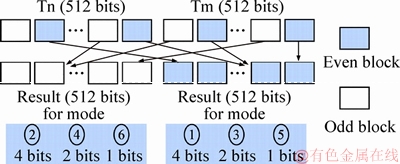
Figure 4 Six patterns of bit interleaving
3.3.2 Data type conversion instruction
Many bit-level insertion and deletion operations are included in some operators, which is difficult for DSP to process directly. According to the parallelization scheme, the data have to be converted between bits and bytes to process in bytes. The implementation of the above functions is done by the shuffle unit because it is the only component that connects the SIMD vector elements. The instructions are shown in Eq. (8). The symbol (b2B) represents bits to bytes. The symbol (B2b) represents bytes to bits.
 (8)
(8)
4 Redirected register file
The distributed register file is used by WANG et al [5]. This architecture can improve the algorithmic performance. It makes each FU accessible to any other FU. But the internetwork becomes very complex. It also leads to an overhead in timing and power consumption. Most studies [12-14] start from the structure of the internetwork. They optimize latency and power via optimal clustering. Rarely research has been optimized from the hardware architecture of the register file. The interface between the internetwork and the FU is the distributed register file. The latency and power generated by the internetwork have a great relationship with the interface of the register file.
4.1 Hardware structure
The architecture of the redirected register file [15] is to implement distributed register files. Figure 5(a) shows the general distributed register file architecture. It has multiple levels of MUX logic at the write port, which causes a certain latency. The redirected register file binds the write port directly to the input of a physical register, as shown in Figure 5(b). In the current cycle, if the enable of the write port is valid, the data will be written directly into the register unconditionally. The existing data in the register should be judged. If the data are overwritten in a logical sense, no scheduling is required; otherwise, the data must be dispatched to other registers by the scheduling logic.
Thus, the latency between the internetwork and the write port of register file is transferred to the scheduling logic latency between the register and register. The latency of scheduling the network is not shared with other logic for one clock cycle. The latency at the write port is reduced to a level of MUX logic latency, which is conducive to the improvement of the frequency. It also reduces the fan out of the data bus at the register file, which reduces power at the same time.
Figure 5 Traditional register file (a) and redirected register file (b)
Each register��s physical and logical meaning of the traditional structure in Figure 5(a) are the same, that is, the data stored in each register physical represents the data stored in the logic register. The same property applied to the structure in Figure 5(b) obviously leads to data storage errors. Therefore, the structure of register and the way of data stored must be changed. Figure 6 shows the structure of the redirected register file. High-K bits are logic tags that represent the tag of the logic register. The lower M bits represent the data stored in the register represented by the logic tag.
Figure 6 Structure of redirected register
4.2 Dynamic scheduling scheme
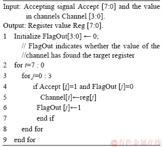
To ensure that no conflict occurs during scheduling, a scheduling scheme is designed. Two types of registers are determined at first. The first type is a register in which stored data have to be dispatched. The second type is a free register that can accept data. In the example given by YANG et al [15], the number of channels is 4. The logic that writes the data in the first type of register to the 4 channels is called entry logic, as shown in Figure 7(a). The logic that sends the data in the channel to the second type of register is called exit logic, as shown in Figure 7(b).
To eliminate conflicts, the priorities of entry logic and exit logic are determined. Taking an 8-depth register file as an example, the priority algorithm for entry logic is shown in Algorithm 1. The exit logic is shown in Algorithm 2. There is no conflict in scheduling with the dynamic scheduling scheme.
Figure 7 Diagrams of entry logic (a) and exit logic (b)
Algorithm 1: Entry priority
Algorithm 2: Exit priority
5 Two-dimensional code compression
MaPU is a VLIW DSP that requires a large amount of instruction memory resources due to its long instruction width, which requires a large instruction memory space. JIN et al [16] and VIITANEN et al [17] proposed some code compression schemes, but these studies were oriented to one-dimensional (horizontal) code compression. They do not consider vertical compression. For the VLIW machine, the code is two-dimensional. Horizontal dimension codes are used for different slots in the same cycle. The vertical dimension codes are used for different cycles in the same slot. A two-dimensional code compression scheme is proposed. The code is compressed in both horizontal and vertical dimensions to remove no operation (NOP) and save memory space.
5.1 Vertical compression
For the VLIW machine, the amount of FUs used in each cycle is limited. Some instruction slots will have consecutive NOPs that occupy a large amount of memory space, as shown in Figure 8(a). To solve such a long series of continuous NOPs, the wait instruction is proposed. The syntax is shown in Figure 8(b). The parameter is a 6-bit immediate data indicating how many cycles of subsequent instructions are delayed to emit. It supports delayed emission from 0 to 63 cycles. Figure 8(a) shows the original code. There are 5 NOPs between the two valid instructions. Figure 8(b) shows the vertically compressed code. Five NOPs are replaced by a wait@5. It can replace up to 63 NOPs. The fetch component of the processor decodes the wait instruction in advance. The next instruction is delayed to emit according to the immediate value in the instruction. Such a design has a significant effect on the code of successive long strings of NOPs.
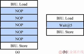
Figure 8 Diagrams of before vertical compression (a) and after vertical compression (b)
Figure 9 shows the implementation of the wait instruction with a FIFO of 63-depth. The fetch component loads the instructions in each slot into the corresponding FIFO. When the program starts, the address indicated by the read pointer (RPointer) of the FIFO is the same as the address indicated by the write pointer (WPointer). The fetch component sends the instruction read from the memory, instead of the one read from FIFO, directly to the FUs. The fetch component will decode the wait instruction in advance and extract the immediate value (WaitNum). There is a counter (WaitCount) in the fetch component. And the value of this counter is initialized as Eq. (9). The value of WaitCount is then decremented by one every cycle until it is reduced to zero.
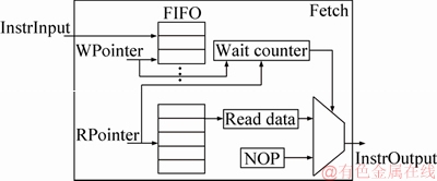
Figure 9 Wait instruction implementation.
WaitCount=WaitNum-(WPointer-RPointer) (9)
At this point, the read pointer will also be adjusted as Eq. (10).
RPointer=WPointer-WaitNum (10)
The read pointer and write pointer plus 1 for each cycle. When the WaitCount is not reduced to 0, the fetch component continues to send a NOP to the FU. When the counter is decremented to 0, it starts sending instructions read from the FIFO. Each time a wait instruction occurs, the internal counter and read pointer are adjusted as Eqs. (9) and (10).
5.2 Horizontal compression
The length of the VLIW instruction is fixed. Each instruction contains the binary codes of 17 slots, which are extremely long. Considering that only few instruction slots actually have valid instruction, a lot of redundant space exists.
A 21-bit description segment is added to the 17 instruction slots by compiler, as shown in Figure 10. Bits 0 to 16 of the description segment indicate whether the instruction slot contains a valid instruction or a NOP. Bit 0 indicates the NOP. Bit 1 indicates the valid instruction. Bits 17-20 of the description segment indicate the number of words after compression. If the total number of bits is not an integer (in words) after compression, several bits 0 are added to the upper bits to complement the whole word. After the fetch component obtains instruction from the memory, it will restore NOP according to the description segment.
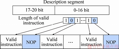
Figure 10 Horizontal compression
6 Diverse access mode
The memory access mode described by WANG et al [5] is a highlight. It supports multidimensional row and column access that greatly improves the efficiency of matrix calculation. Considering the special requirements of 5G baseband processing, some special-access modes have to be supported. Based on the original memory of MaPU, two new types of memory access modes are proposed.
6.1 Discrete access mode
Many baseband processing algorithms such as PN sequence generation, cyclic redundancy check (CRC) and QAM can be easily parallelized by lookup. Some nonlinear functions can also be completed more efficiently by lookup. Therefore, discrete access instruction is proposed to efficiently support such lookup. The data of each bank is accessed independently according to the index value. Register-related configuration in bus interface unit (BIU) for memory access is described [5]. The granularity parameter G is set to 6 and 512 bits of 64 blocks are accessed in parallel. The address is discrete. The base address and the offset address determine the access address of each byte. For example, if the base address is set to KB=0, the offset address is stored in T register. The accessed data are shown in Figure 11(a).
6.2 Interval access mode
Many complex numbers are processed by baseband. Data are stored and calculated by the processor in both real and imaginary parts. These real and imaginary parts are stored in intervals. The row and column access mode in MaPU does not support separate access to real or imaginary parts. An interval access mode is proposed. This access mode can support interval access instead of continuous access. The interval step is determined according to the data type of the real part and the imaginary part. The required data can be removed separately. As shown in Figure 11(b), 64 blocks is accessed in parallel. The real and imaginary data type are 16-bit halfwords. All real parts (blue data blocks) can be accessed by interval access mode. The interval access mode enable register StepEnable is set to 1, G=1, and KB=0. The vector is shown in Figure 11(b).
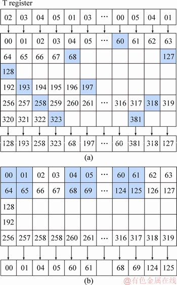
Figure 11 Discrete access mode (a) and interval access mode (b)
7 Implementation and evaluation
UCP is synthesized with Design Compiler of Synopsys in a 16-nm logic library. The net-list then generates a layout by IC Compiler of Synopsys, as shown in Figure 12. The clock frequency is 1.4 GHz. The design of UCP is based on the coarse- grained reconfigurable architecture (CGRA). The algorithm is all soft-implemented. The structure of the hardware pipeline is configured by the software. For example, the pipeline configuration of the polar encoding algorithm is shown in Figure 13. Thus, the accelerator module of the specific algorithm is deleted compared with MaPU. There are many fixed-point and bit-level operations in communication. Floating-point operations are also implemented by fixed-point operations. Thus,compared to MaPU, fixed-point and bit-level operations are added into two floating-point units (IFALU and IFMAC). The floating-point operations are simplified. The number of shuffle units also increased from 2 to 3. All FUs are the low power consumption structure with highly reused hardware. The silicon area evaluated by the layout is 5.8 mm2, which is 1/6 of the MaPU��s. The average power consumption is 0.7 W, which is 1/5 of the MaPU��s.
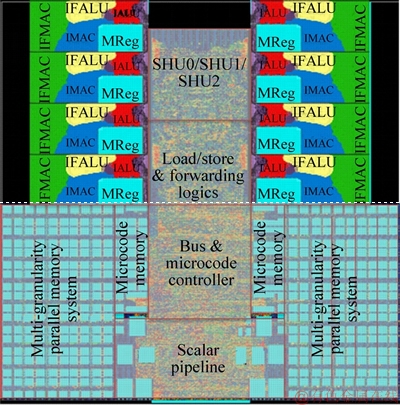
Figure 12 Layout of UCP
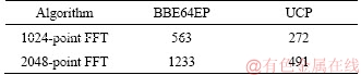
Various 5G baseband processing algorithms are implemented on the single core of UCP to get its performance. Because the performance of CEVA's XC12 has not yet been gotten, the performance is compared with the TMS320C6670, UCP greatly improves the algorithmic performance of the 5G baseband processing. The performance of each algorithm exceeds the TMS320C6670 by an order of magnitude with less power consumption, as shown in Figure 14(a). The performance-to- power ratio of the UCP core and C66x core during algorithm execution is shown in Figure 14(b). The FFT execution cycle is compared with BBE64EP, as shown in Table 1. UCP achieves high throughput and meets the real-time requirements of the 5G standard.
UCP can greatly improve the algorithmic throughput. Several factors are involved:
1) Wide width SIMD and multiple FUs are conducive to the development of algorithmic parallelism;
2) At high frequency of 1.4 GHz, the single- core processing capacity can reach 358 GOPS@16 bit;
3) The specific design is needed for the 5G baseband processing algorithm by the dedicated instruction. The support of the bit-level processing accelerates the efficiency with which the algorithm is implemented;
4) Customized multi-granular memory data shuffle units are required to ensure a flexible and efficient data supply for communication-specific instruction operations.
Figure 13 Pipeline configuration of polar encoding
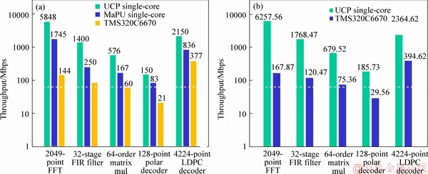
Figure 14 Performance comparison with TMS320C6670 (a) and performance-to-power ratio (b)
Table 1 FFT execution cycle comparison with BBE64EP
8 Conclusions
Based on MaPU, the computing architecture is proposed for 5G baseband processing in this work, the optimization includes four aspects.
1) The FUs are designed for 5G baseband processing. A series of 5G dedicated instructions are proposed;
2) A redirected register file is proposed for the timing and power consumption issues in internetwork;
3) In the case of memory space wasted, a two-dimensional code compression scheme and implementation are proposed for the VLIW architecture;
4) For the characteristics of the data type and algorithm in 5G baseband processing, the access mode of the data memory is extended.
With these optimizations, the UCP has the silicon area of only 1/6 that of the MaPU. The average power consumption is only 1/5 that of the MaPU. The algorithmic performance of the 5G baseband processing is ahead of industry levels. Its throughput exceeds that of TMS320C6670 by one or two orders of magnitude with less power consumption. It is a high-performance and low-power 5G baseband computing architecture with a flexible CGRA that meets the real-time and stability requirements of future 5G communication systems.
References
[1] ZIEGLER V, THEIMER T, SARTORI C, PRADE J, SPRECHER N, ALBAL K, BEDEKAR A. Architecture vision for the 5G era [C]// IEEE International Conference on Communications Workshops. IEEE, 2016: 51-56. DOI: 10.1109/ICCW.2016.7503763.
[2] GONZALEZ-PLAZA A, MORENO J, VAL I, ARRIOLA A, RODRIGUEZ P M, JIMENEZ F, BRISO C. 5G communications in high speed and metropolitan railways [C]// European Conference on Antennas and Propagation. IEEE, 2017: 658-660. DOI: 10.23919/EuCAP.2017. 7928756.
[3] DEHON A, WAWRZYNEK J. Reconfigurable computing:what, why, and implications for design automation [C]// Proc Design Automation Conference. 1999: 610-615. DOI: 10.1109/DAC.1999.782016.
[4] FERREIRA M L, FERREIRA J C. Reconfigurable NC-OFDM processor for 5G communications [C]// International Conference on Embedded and Ubiquitous Computing. IEEE, 2015: 199-204. DOI: 10.1109/EUC. 2015.29.
[5] WANG Dong-lin, XIE Shao-lin, ZHANG Zhi-wei, DU Xue- liang, WAND Lei, LIU Zi-jun, LIN Xiao, HAO Jie, YIN Lei-zu, WANG Tao, YANG Yong-yong, LIN Chen, MA Hong Ma, PU Zhong-hua, DING Guang-xin, SUN Wen-qin, ZHOU Fa-biao, REN Wei-li, WANG Hui-juan Wang, ZHU Meng-chen, YANG Li-peng, XIAO Nuo-Zhou, CUI Qian Cui, WANG Xin-gang, GUO Ruo-shan Guo,WANG Xiao- qin. MaPU: A novel mathematical computing architecture [C]// IEEE International Symposium on High Performance Computer Architecture. IEEE, 2016: 457-468. DOI: 10.1109/HPCA.2016.7446086.
[6] KANTEE D. CEVA Telegraphs 5G intent with XC12 [EB/OL]. [2019-4-21]. https://www.ceva-dsp.com/wp- content/uploads/2017/04/ Ceva_XC12-MPR-reprint.pdf.
[7] Texas Instruments. TMS320C6670 multicore fixed and floating-point system-on-chip [EB/OL]. [2019-4-21]. http://www.ti.com.cn/cn/lit/ds/ symlink/tms320c6670.pdf.
[8] Cadence. Tensilica ConnX BBE Family of Performance Baseband DSPs [EB/OL]. [2019-4-21]. https://ip. cadence. com/uploads/130/TIP_PB_Connx_DSP_FINAL-pdf.
[9] FENG Jing, LIU Zi-jun, MA Xiao-jun, GUO Yang, GUO Peng, WANG Dong-lin. A reconfigurable high-performance multiplier based on multi-granularity design and parallel acceleration [C]// IEEE International Conference on Software Engineering and Service Science. IEEE, 2017: 567-570. DOI: 10.1109/ICSESS.2017.8342979.
[10] YANG Guo, GUO Yang, XIE Shao-lin, LIU Zi-jun, YANG Lei, WANG Dong-lin. Parallel polar encoding in 5G communication [C]// IEEE Symposium on Computers and Communications. IEEE, 2018. DOI: 10.1109/ISCC. 2018.8538743.
[11] LEROUX C, TAL I, VARDY A, GROSS W J. Hardware architectures for successive cancellation decoding of polar codes [C]// IEEE International Conference on Acoustics, Speech and Signal Processing. IEEE, 2011: 1665-1668. DOI: 10.1109/ICASSP.2011.5946819.
[12] CONG J, FAN Y, XU J. Simultaneous resource binding and interconnection optimization based on a distributed register-file microarchitecture [J]. ACM Transactions on Design Automation of Electronic Systems, 2006, 14(3): 824-833. DOI: 10.1145/1529255.1529257.
[13] HUANG Y S, HONG Y J, HUANG J D. Communication synthesis for interconnect minimization targeting distributed register-file microarchitecture [J]. IEICE Transactions on Fundamentals of Electronics Communications & Computer Sciences, 2011, 94-A(4): 1151-1155. DOI: 10.1587/transfun. E94.A.1151.
[14] HUANG J D, CHEN C I, HSU W L, LIN Y T, JOU J Y. Performance-driven architectural synthesis for distributed register-file microarchitecture considering inter-island delay [C]// Proceedings of 2010 International Symposium on VLSI Design, Automation and Test. IEEE, 2010: 169-172. DOI: 10.1109/VDAT.2010. 5496717.
[15] GUO Yang, WANG Dong-lin, LIU Zi-jun, MENG Hong-yu. A distributed register file architecture based on dynamic scheduling for VLIW machine [C]// International Conference on Electronics Information and Emergency Communication. IEEE, 2018: 67-70. DOI: 10.1109/ICEIEC.2018.8473572.
[16] JIN T, AHN M, YOO D, SUH D, LEE S. Nop compression scheme for high speed DSPs based on VLIW architecture [C]// IEEE International Conference on Consumer Electronics. IEEE, 2014: 304-305. DOI: 10.1109/ICCE.2014.6776016.
[17] HELKALA J, VIITANEN T, KULTALA H, JAASKELAINEN P, BERG H. Variable length instruction compression on transport triggered architectures [C]// International Conference on Embedded Computer Systems: Architectures, Modeling, and Simulation. IEEE, 2018: 149-155. DOI: 10.1109/SAMOS.2014. 6893206.
(Edited by FANG Jing-hua)
���ĵ���
һ������5Gͨ�ŵĿ��ع�����ܹ�
ժҪ��5G�����źŴ�����Ӳ������˸��ߵ�ʵʱ�ԺͿɿ���Ҫ����MaPU����ϵ�ṹ������5G�����źŴ������ص㣬���������һ�ֿ��ع��ļ�����ϵ�ṹ�����ȣ������һ������5G�����źŴ�����ר��ָ������������Ӧ�Ĺ��ܵ�Ԫ��Ӳ����Դ������ƣ�Ȼ��������ض���Ĵ����ļ���������������е��ӳٺ������⡣���ָ��洢����ʹ���ʵ͵����������˶�ά��ѹ������������չ�����ݴ洢���ķ���ģʽ��ʹ���ܵõ����ƣ��������Խ��͡����ܹ���5G���������㷨����������TMS320C6670�߳�һ�����������������ĸ��͡����������Ĺ����Ϊ5.8 mm2����MaPU�����1/6��ƽ������Ϊ0.7 W����MaPU��1/5��
�ؼ��ʣ�5Gͨ�ţ�ָ����Ĵ����ļ�������ѹ���������ʣ�����
Foundation item: Project(XDA-06010402) supported by the Strategic Priority Research Program of Chinese Academy of Sciences; Project (Y5S7061G51) supported by the Youth Innovation Promotion Association of Chinese Academy of Sciences
Received date: 2018-11-14; Accepted date: 2019-03-04
Corresponding author: GUO Yang, PhD; Tel: +86-18701010065; E-mail: guoyang2014@ia.ac.cn; ORCID: 0000-0002-1453-6645

