晶圆级芯片尺寸封装Sn-3.0Ag-0.5Cu焊点跌落失效模式
来源期刊:中国有色金属学报(英文版)2016年第6期
论文作者:黄明亮 赵宁 刘爽 何宜谦
文章页码:1663 - 1669
关键词:Sn-3.0Ag-0.5Cu;晶圆级芯片尺寸封装;焊点;跌落失效模式
Key words:Sn-3.0Ag-0.5Cu; wafer level chip scale package; solder joint; drop failure mode
摘 要:依据JEDEC标准采用板级跌落实验研究晶圆级芯片尺寸封装Sn-3.0Ag-0.5Cu焊点的跌落失效模式。发现存在六种失效模式,即发生在印刷电路板(PCB)侧的短FR-4裂纹和完全FR-4裂纹,以及发生在芯片侧的再布线层(RDL)与Cu凸点化层开裂、RDL断裂、体钎料裂纹及体钎料与界面金属间化合物(IMC)混合裂纹。对于最外侧的焊点,由于PCB变形量较大且FR-4介质层强度较低,易于形成完全FR-4裂纹,其可吸收较大的跌落冲击能量,从而避免了其它失效模式的发生。对于内侧的焊点,先形成的短FR-4裂纹对跌落冲击能量的吸收有限,导致在芯片侧发生失效。
Abstract: To reveal the drop failure modes of the wafer level chip scale packages (WLCSPs) with Sn-3.0Ag-0.5Cu solder joints, board level drop tests were performed according to the JEDEC standard. Six failure modes were identified, i.e., short FR-4 cracks and complete FR-4 cracks at the printing circuit board (PCB) side, split between redistribution layer (RDL) and Cu under bump metallization (UBM), RDL fracture, bulk cracks and partial bulk and intermetallic compound (IMC) cracks at the chip side. For the outmost solder joints, complete FR-4 cracks tended to occur, due to large deformation of PCB and low strength of FR-4 dielectric layer. The formation of complete FR-4 cracks largely absorbed the impact energy, resulting in the absence of other failure modes. For the inner solder joints, the absorption of impact energy by the short FR-4 cracks was limited, resulting in other failure modes at the chip side.
Trans. Nonferrous Met. Soc. China 26(2016) 1663-1669
Ming-liang HUANG1, Ning ZHAO1, Shuang LIU1, Yi-qian HE2
1. School of Materials Science and Engineering, Dalian University of Technology, Dalian 116024, China;
2. Department of Engineering Mechanics, Dalian University of Technology, Dalian 116024, China
Received 5 June 2015; accepted 3 December 2015
Abstract: To reveal the drop failure modes of the wafer level chip scale packages (WLCSPs) with Sn-3.0Ag-0.5Cu solder joints, board level drop tests were performed according to the JEDEC standard. Six failure modes were identified, i.e., short FR-4 cracks and complete FR-4 cracks at the printing circuit board (PCB) side, split between redistribution layer (RDL) and Cu under bump metallization (UBM), RDL fracture, bulk cracks and partial bulk and intermetallic compound (IMC) cracks at the chip side. For the outmost solder joints, complete FR-4 cracks tended to occur, due to large deformation of PCB and low strength of FR-4 dielectric layer. The formation of complete FR-4 cracks largely absorbed the impact energy, resulting in the absence of other failure modes. For the inner solder joints, the absorption of impact energy by the short FR-4 cracks was limited, resulting in other failure modes at the chip side.
Key words: Sn-3.0Ag-0.5Cu; wafer level chip scale package; solder joint; drop failure mode
1 Introduction
The approaches of miniaturization, light weight, high speed, and multifunction will be never-ending for electronic devices, which definitely results in higher density and smaller dimension of electronic package. To meet these increasing requirements from both market and technique, great efforts have been implemented to develop advanced packaging technologies. With simplified process, high production efficiency, reduced cost and small footprint, wafer level chip scale package (WLCSP) has become one of the most attractive emerging package technologies, especially in portable consumer market [1,2].
In electronic packaging, solder alloys are still the most commonly used interconnection materials. Due to the serious environmental and public health concerns on Pb, lead-free solders have been developed to substitute the traditional Sn-Pb solders [3,4]. So far, Sn-Ag-Cu alloys, typically Sn-3.0Ag-0.5Cu (SAC305), have been proved to be the most popular lead-free solders [5-7]. Since portable consumer electronics are frequently shocked and dropped in service, crack and even fracture may occur in solder joints or package substrate, which seriously degrades the reliability of the products. Hence, drop failure modes and mechanisms of solder joints as well as package substrate are quite important for product design and manufacturing.
Many studies on the drop reliability of Sn-Ag-Cu solder joints have been carried out. LAI et al [8] pointed out that solder joints with a low Ag content and substrate pads with organic solderability preservative (OSP) surface finish (another was Ni/Au) both enhanced the drop resistance of the board-level test vehicle. Besides, the failure mode statistics indicated that most of fractures located on the package side for high Ag content solder joints while on the test board side for low Ag content ones. SUH et al [9] reported that Sn-4.0Ag-0.5Cu solder typically exhibited interfacial fracture during drop testing, while Sn-1.0Ag-0.5Cu solder exhibited considerable amount of cohesive failure through bulk solder. The effects of minor alloying elements, such as Ni, Ge, Zn, Pd, In, Co, and Fe, on the failure modes of Sn-Ag-Cu solders in terms of drop impact and thermal cycling have also been investigated [10-13].
The structure of a package also plays an important role in the drop reliability. TUMNE et al [14] found that smaller array size, pitch and package height showed better drop reliability. FAN et al [15] reported that for a copper post (or pillar) wafer level package, wafer level epoxy, which encapsulated copper pillars, served as a compliant layer for solder joint stress reduction under dynamic loading. An elasto-plastic model was applied on both solder bump and copper pad materials to simulate the drop performance of WLCSPs and a good accuracy was obtained [16].
Up to now, few studies focus on the board level drop performance of WLCSPs with Sn-3.0Ag-0.5Cu solder joints, which is significant for the design and reliability evaluation of portable consumer electronics. In the present work, board level drop tests were performed using WLCSPs with Sn-3.0Ag-0.5Cu solder joints and the failure modes were identified and discussed.
2 Experimental
WLCSP products with real chips were used as the board level drop test samples. No underfill was used for these WLCSP products. Figure 1(a) shows a WLCSP specimen with four chips mounted on the printing circuit board (PCB). The PCB consisted of nine copper trace layers with FR-4 as the dielectric layers. The dimensions of the chips were 5.33 mm × 4.89 mm × 0.31 mm and those of the PCB were 100 mm × 50 mm × 0.78 mm. Four positioning holes with a diameter of 3 mm were fabricated at the corners of the PCB to fix the samples on the drop tester with the chips facing down. The horizontal distance between the positioning holes was 97 mm and the vertical distance was 40 mm.
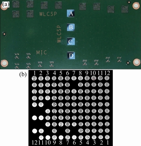
Fig. 1 WLCSP specimen (a) and X-ray image of chip (b)
The composition of the solder balls was Sn-3.0Ag-0.5Cu. The pads with 250 μm in diameter on the PCB side was OSP-Cu with non solder mask defined (NSMD) and the under bump metallizations (UBMs) on the chip side were Cu. The Cu UBMs were fabricated on redistribution layer (RDL). Figure 1(b) shows the X-ray image of one of the chips, clearly showing the configuration and array of the solder balls. Pores existed in some of the solder balls. The average diameter of the solder balls was 300 μm with a standoff height of 155 μm and a pitch of 400 μm.
Board level drop tests were carried out using CL20 impact test system according to the Joint Electron Devices Engineering Council (JEDEC) standard for drop testing―JESD22-B111 [17] and JESD22-B104C [18]. The drop tests were performed under a peak acceleration of 2900g (where g is 9.8 N/kg) and a pulse duration of 0.3 ms for 5000 drop times. After the drop tests, the WLCSPs were ground and polished for cross-sectional observation using a scanning electron microscope (SEM), in order to identify the failure modes. The deformation and stress in the WLCSPs were simulated using ABAQUS, in which the model was built using real geometric size and the properties such as density, elastic modulus, and Poisson’s ratio were set using the values for real materials. The acceleration was applied on the centre of gravity of the test sample.
3 Results and discussion
3.1 Microstructure of as-soldered WLCSP
Figure 2 shows the cross-sectional SEM images of an as-soldered WLCSP sample. As shown in Fig. 2(a), intact interconnections were achieved between the chip and the PCB by the well formed solder joints. Figure 2(b) shows the microstructure of a solder joint in Fig. 2(a). A continuous intermetallic compound (IMC) layer formed at each interface of solder/Cu pad and solder/Cu UBM.
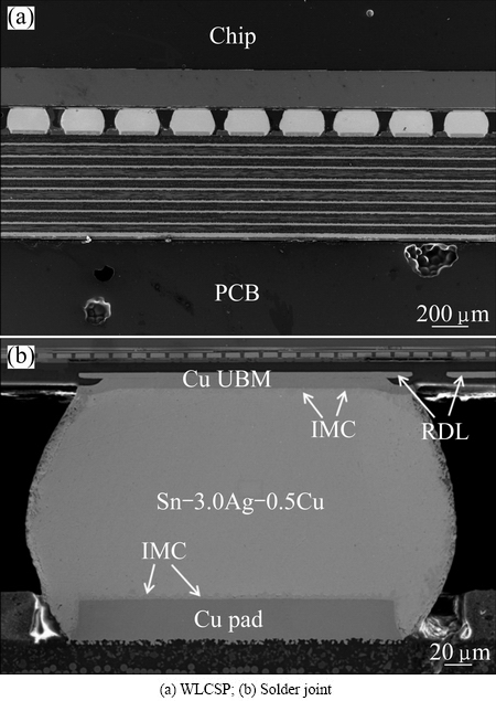
Fig. 2 Cross-sectional microstructures of as-soldered sample
3.2 Failure modes under 2900g and 0.3 ms
To reveal the failure behavior, the WLCSP was dropped under 2900g and 0.3 ms for 5000 times. Figure 3 shows the schematic of the failure modes in the failed WLCSPs. Modes 1-6 represent short FR-4 crack, complete FR-4 crack, split between RDL and Cu UBM, RDL fracture, bulk crack and partial bulk solder and IMC crack, respectively.
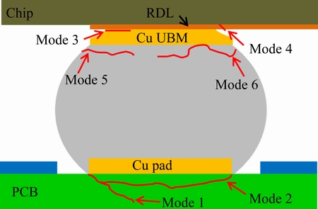
Fig. 3 Schematic of failure modes in failed WLCSPs
Figure 4 shows the microstructure of No. 1 solder joint of Chip A and the enlarged images at the corners. Failure modes 1, 3 and 4 were identified, i.e., short FR-4 crack at the PCB side (Fig. 4(b)), split between RDL and Cu UBM at the chip side (Fig. 4(c)), and RDL fracture at the corner underneath the Cu UBM (Fig. 4(d)). It is noted that the FR-4 crack derived from the outer edge of the Cu pad, propagated in the FR-4 dielectric layer along a direction of 45° and then divided into two cracks, with one propagating along the original direction toward the Cu trace layer and the other propagating parallel to the Cu pad.
Figure 5 shows the microstructure of solder joint No. 3 of Chip A and the enlarged image at the chip side. A crack propagated in the bulk solder near the Sn-3.0Ag-0.5Cu/Cu UBM interface, i.e., failure mode 5, occurred. Since the impact was larger where it was further from the center of the chip, the bulk crack must initiate at the outer edge of the solder and propagate into the solder parallel to the interface. The failure modes in solder joint No. 3of Chip A were quite different from those in solder joint No. 1 of Chip A, i.e., no FR-4 crack was observed at the PCB side. Compared with the outer solder joints, the deformation of the PCB underneath solder joint No. 3 during each drop was relatively small, resulting in a low impact stress.
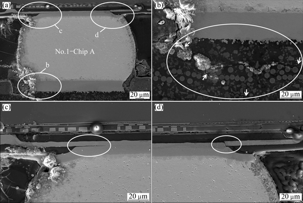
Fig. 4 Microstructure of solder joint No. 1 of Chip A (a) and enlarged images (b-d) at corners b-d in Fig. 4(a), respectively
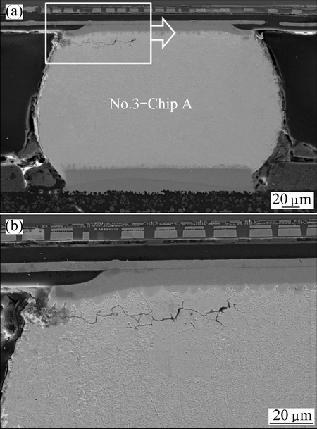
Fig. 5 (a) Microstructure of solder joint No. 3 of Chip A (a) and enlarged image at chip side (b)

Fig. 6 Microstructure of solder joint No. 12 of Chip A
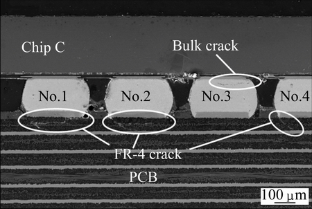
Fig. 7 Overall microstructure of solder joints Nos. 1-4 of Chip C
Figure 6 shows the microstructure of solder joint No. 12 of Chip A. A large FR-4 crack formed which connected the two edges of the Cu pad formed, i.e., failure mode 2 occurred. However, the solder joint remained intact. It seems that if a complete FR-4 crack formed, no other failure mode would occur.
Figure 7 shows the overall microstructure of solder joints Nos. 1-4 of Chip C. Short FR-4 crack (No. 4), complete FR-4 crack (Nos. 1 and 2), split between RDL and Cu UBM (No. 3), and bulk crack (No. 3) occurred in the WLCSP. Figure 8 shows the microstructures of solder joints Nos. 1, 3 and 11of Chip C. For solder joint No. 1, the complete FR-4 crack initiated at the outer edges of the Cu pads and propagated toward the middle of the FR-4 dielectric layer along a direction of 45°. Thereafter, as indicated by the arrow in Fig. 8(b), the crack divided into two cracks. One propagated along the original direction to reach the Cu trace layer, and the other propagated parallel to the Cu pad and finally reached the opposite edge. The same phenomenon was also observed in solder joint No. 11, where the complete FR-4 crack propagated from the right to the left. For solder joint No. 3, both split between RDL and Cu UBM and bulk crack were clearly observed at the chip side while no FR-4 crack occurred, which was similar to solder joint No. 3 of Chip A shown in Fig. 5.
Figure 9 shows the microstructures of solder joints Nos. 3, 10 and 11 of Chip D. For solder joint No. 3, a crack initiated at the inner edge of the solder and propagated along a mixture of the bulk solder and the solder/IMC layer interface, i.e., failure mode 6 occurred. The length of this crack exceeded 2/3 of the solder ball diameter. Similar to solder joints No. 3 of other chips, no FR-4 crack occurred at the PCB side. For solder joint No. 10, failure modes 1 and 3 occurred, which were similar with those for solder joint No. 1 of Chip A. For solder joint No. 11, a complete FR-4 crack was observed and there were no other failures. Besides, failure mode 2 also occurred for solder joint Nos. 1 and 2 of Chip D. Combining Figs. 6, 8 and 9, it is noted that no failure occurred at the chip side or in the solder joint when a complete FR-4 crack was generated for the outmost solder joints. It was concluded that the formation of complete FR-4 crack could largely absorb the impact energy, resulting in the absence of other failure modes.
Table 1 presents the failure modes occurred in the tested WLCSPs under 2900g and 0.3 ms. Combining all the dropped WLCSPs, no failure was observed neither in the chips nor at the solder/Cu pad interface, showing good drop reliability. Though silicon is brittle, it also owns a high tensile strength, and most of the impact energy was absorbed by the PCB and solder joints, which guaranteed the integrity of the chips. FR-4 crack at the PCB side was identified to be the dominant failure mode of the present WLCSPs, since it existed in all the failure samples. It was also noted that all the dropped samples in the present study were non SMD. There existed a gap between the solder joint and the solder mask after soldering. Obviously, the gap was a weak region and tended to generate stress concentration due to the appearance of several interfaces undergoing drop test. Therefore, the FR-4 crack was always found to initiate at the edge of Cu pad.
Moreover, all the complete FR-4 cracks occurred underneath the outer solder joints and short FR-4 cracks occurred underneath inner solder joints. During the drop test, the deformation of the FR-4 dielectric layer underneath the inner solder joints, such as Nos. 3, 4 and 10, was smaller than that underneath the outmost ones, such as Nos. 1 and 12, which induced a less serious damage. Figure 10 shows the simulated distributions of deformation and stress in a WLCSP at the peak acceleration. It is clearly shown that the maximum stress located at the corners of the chips, which agreed well with the present results and the report by JESD22-B111 [17] as well. Once a complete FR-4 crack was generated under a solder joint, the impact energy could be largely absorbed by this complete FR-4 crack, and consequently no other failure mode occurred in the solder joint. However, if a short FR-4 crack or no FR-4 crack formed under a solder joint, since the absorption of impact energy by this short FR-4 crack was limited, the impact acted on the solder joint was still large. As a result, the failures such as split between RDL and Cu UBM, RDL fracture, bulk crack and partial bulk and IMC crack occurred at the chip side. Therefore, underfill that can absorb impact energy and consequently protect the solder joints seems quite important to improve the drop reliability of WLCSP.
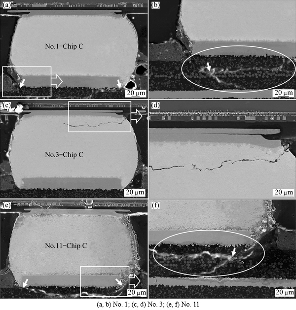
Fig. 8 Microstructures of solder joints of Chip C
Table 1 Failure modes in failed WLCSPs after 5000 drops under 2900g and 0.3 ms

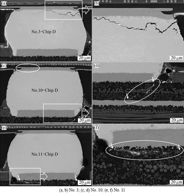
Fig. 9 Microstructures of solder joints of Chip D
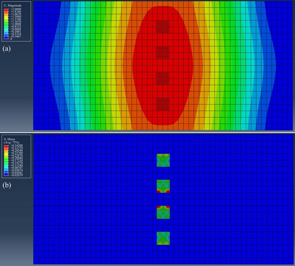
Fig. 10 Simulated distributions of deformation (a) and stress (b) in WLCSP at peak acceleration
4 Conclusions
1) Under the peak acceleration of 2900g and the pulse duration of 0.3 ms, short FR-4 cracks and complete FR-4 cracks at the PCB side, split between RDL and Cu UBM, RDL fracture, bulk cracks and partial bulk and IMC cracks at the chip side were identified. FR-4 cracks were considered as the dominant failure mode in the present WLCSPs.
2) Longer FR-4 cracks occurred for the outer solder joints, and complete FR-4 cracks were usually observed underneath the outmost solder joints. The formation of complete FR-4 cracks could largely absorb the impact energy, resulting in the absence of the other failure modes.
3) Short FR-4 cracks generally occurred underneath the inner solders. The absorption of the impact energy by the short FR-4 cracks was limited, resulting in other failure modes, i.e., split between RDL and Cu UBM, RDL fracture, bulk crack and partial bulk and IMC crack, at the chip side.
References
[1] AHMER S, KARTHIKEYAN D, CHRISTOPHER B, ROBERT M, RIKI W. Electromigration reliability and current carrying capacity of various WLCSP interconnect structures [C]//Proceedings of 63rd Electronic Components and Technology Conference. Las Vegas: IEEE Components, Packaging and Manufacturing Technology Society, 2013: 714-724.
[2] ZHANG Liang, HAN Ji-guang, GUO Yong-huan, HE Cheng-wen. Anand model and FEM analysis of SnAgCuZn lead-free solder joints in wafer level chip scale packaging devices [J]. Microelectronics Reliability, 2014, 54(1): 281-286.
[3] ZHANG Cheng, LIU Si-dong, QIAN Guo-tong, ZHOU Jian, XUE Feng. Effect of Sb content on properties of Sn-Bi solders [J]. Transactions of Nonferrous Metals Society of China, 2014, 24(1): 184-191.
[4] HUANG Ming-liang, ZHOU Qiang, ZHAO Ning, CHEN Lei-da. Interfacial microstructure and mechanical properties of In-Bi-Sn lead-free solder [J]. Journal of Materials Science: Materials in Electronics, 2013, 24(7): 2624-2629.
[5] ZHANG Liang, XUE Song-bai, GAO Li-li, ZENG Guang, CHEN Yan, YU Sheng-lin, SHENG Zhong. Creep behavior of SnAgCu solders with rare earth Ce doping [J]. Transactions of Nonferrous Metals Society of China, 2010, 20(3): 412-417.
[6] GAN Gui-sheng, DU Chang-hua, XU Hui-bin, YANG Bin, LI Zheng-kang, WANG Tao, HUANG Wen-chao. Low-temperature soldering technology with stirring for nano-Ni particle-reinforced lead-free Sn-Cu-Ag composite solders [J]. The Chinese Journal of Nonferrous Metals, 2013, 23(10): 2875-2881. (in Chinese)
[7] HUANG Ming-liang, YANG Fan, ZHAO Ning, YANG Yao-chuan. Synchrotron radiation real-time in situ study on dissolution and precipitation of Ag3Sn plates in sub-50 μm Sn-Ag-Cu solder bumps [J]. Journal of Alloys and Compounds, 2014, 602: 281-284.
[8] LAI Y S, YANG P F, YEH C L. Experimental studies of board-level reliability of chip-scale packages subjected to JEDEC drop test condition [J]. Microelectronics Reliability, 2006, 46(2-4): 645-650.
[9] SUH D, KIM D W, LIU P L, KIM H, WENINGER J A, KUMAER C M, PRASAD A, GRIMSLEY B W, TEJADA H B. Effects of Ag content on fracture resistance of Sn-Ag-Cu lead-free solders under high-strain rate conditions [J]. Materials Science and Engineering A, 2007, 460-461: 595-603.
[10] LAI Y S, SONG J M, CHANG H C, CHIU Y T. Ball impact responses of Ni- or Ge-doped Sn-Ag-Cu solder joints [J]. Journal of Electronic Materials, 2008, 37(2): 201-209.
[11] SON J Y, LEE Y W, HONG S J, IM I B, LEE J H, KIM H J, MOON J T. Study on the characteristics of various dopants in Sn-1Ag-0.8Cu solder [C]//Proceedings of 13th Electronics Packaging Technology Conference. Singapore: IEEE Computer Society, 2011: 231-235.
[12] SHNAWAH D A, SAHBI M F M, BADRUDDIN I A. A review on thermal cycling and drop impact reliability of SAC solder joint in portable electronic products [J]. Microelectronics Reliability, 2012, 52(1): 90-99.
[13] SHNAWAH D A, SAHBI M F M, BADRUDDIN I A, SAID S B M, ARIGA T, CHE F X. Effect of Ag content and the minor alloying element Fe on the mechanical properties and microstructural stability of Sn-Ag-Cu solder alloy under high-temperature annealing [J]. Journal of Electronic Materials, 2013, 42(3): 470-484.
[14] TUMNE P, VENKATADRI V, KUDTARKAR S, DELAUS M, SANTOS D, HAVENS R, SRIKARI K. Effect of design parameters on drop test performance of wafer level chip scale packages [J]. Journal of Electronic Packaging, 2012, 134(2): 020905.
[15] FAN X J, RANOUTA A S, DHIMAN H S. Effects of package level structure and material properties on solder joint reliability under impact loading [J]. IEEE Transactions on Components, Packaging and Manufacturing Technology, 2013, 3(1): 52-60.
[16] COQ C L, ADELLAH T, STEMPIN M P, BARREAU L. Optimization for simulation of WL-CSP subjected to drop-test with plasticity behavior [J]. Microelectronics Reliability, 2011, 51(6): 1060-1068.
[17] JEDEC Standard JESD22-B111. Board level drop test method of components for handheld electronic products [S].
[18] JEDEC Standard JESD22-B104C. Mechanical shock [S].
黄明亮1,赵 宁1,刘 爽1,何宜谦2
1. 大连理工大学 材料科学与工程学院,大连 116024;
2. 大连理工大学 力学工程系,大连 116024
摘 要:依据JEDEC标准采用板级跌落实验研究晶圆级芯片尺寸封装Sn-3.0Ag-0.5Cu焊点的跌落失效模式。发现存在六种失效模式,即发生在印刷电路板(PCB)侧的短FR-4裂纹和完全FR-4裂纹,以及发生在芯片侧的再布线层(RDL)与Cu凸点化层开裂、RDL断裂、体钎料裂纹及体钎料与界面金属间化合物(IMC)混合裂纹。对于最外侧的焊点,由于PCB变形量较大且FR-4介质层强度较低,易于形成完全FR-4裂纹,其可吸收较大的跌落冲击能量,从而避免了其它失效模式的发生。对于内侧的焊点,先形成的短FR-4裂纹对跌落冲击能量的吸收有限,导致在芯片侧发生失效。
关键词:Sn-3.0Ag-0.5Cu;晶圆级芯片尺寸封装;焊点;跌落失效模式
(Edited by Mu-lan QIN)
Foundation item: Projects (51475072, 51171036) supported by the National Natural Science Foundation of China
Corresponding author: Ming-liang HUANG; Tel: +86-411-84706595; Fax: +86-411-84709284; E-mail: huang@dlut.edu.cn
DOI: 10.1016/S1003-6326(16)64272-3

