Microstructure and Radiation Damage of Cu-Nb Alloy Thin Films
Yu Kaiyuan Li Yan Sun Yifan Zhang Gan Zhang Zhanxuan
College of New Energy and Materials,China University of Petroleum-Beijing
Abstract��
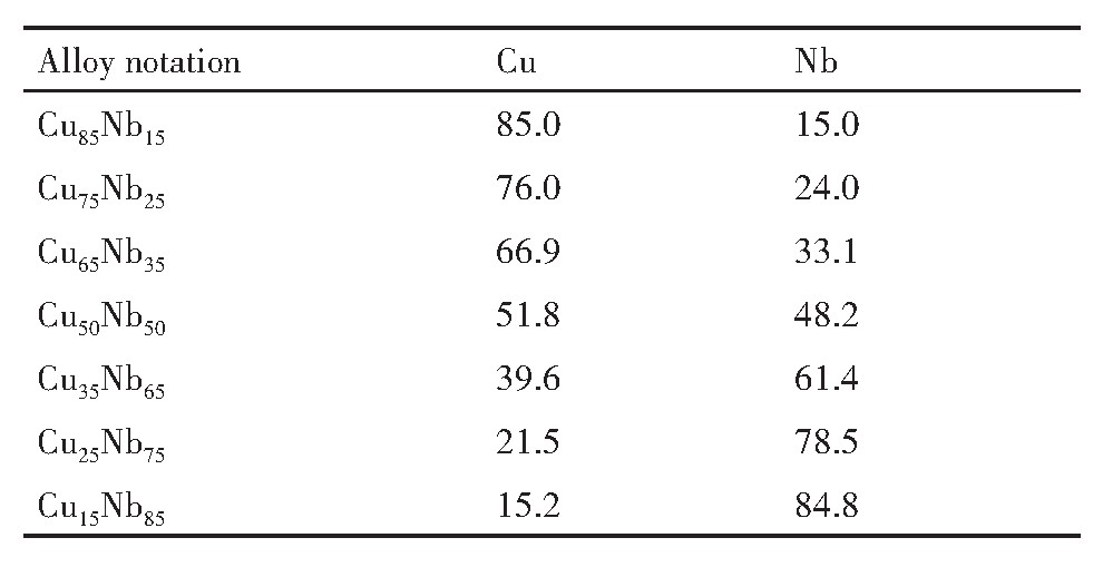
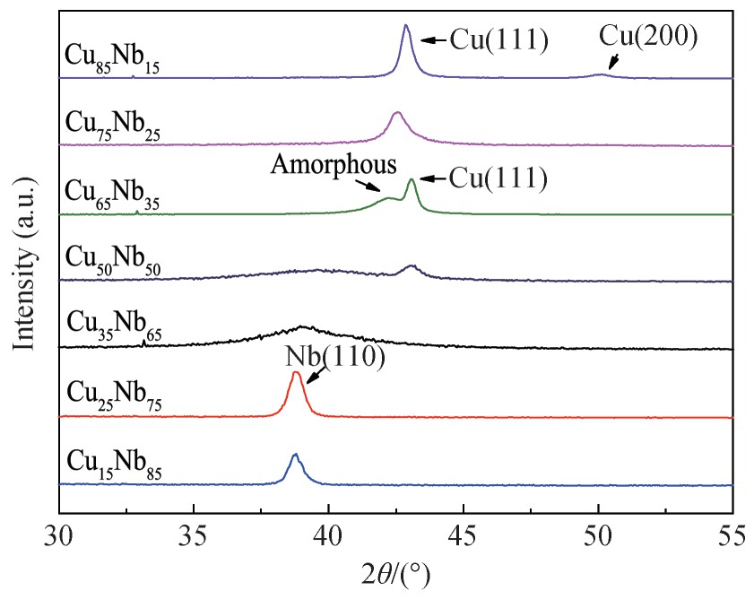
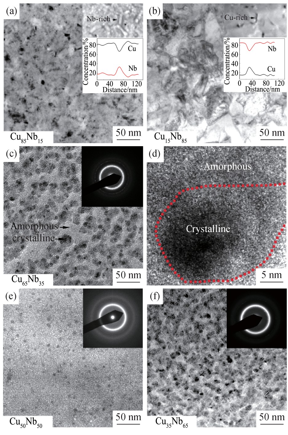
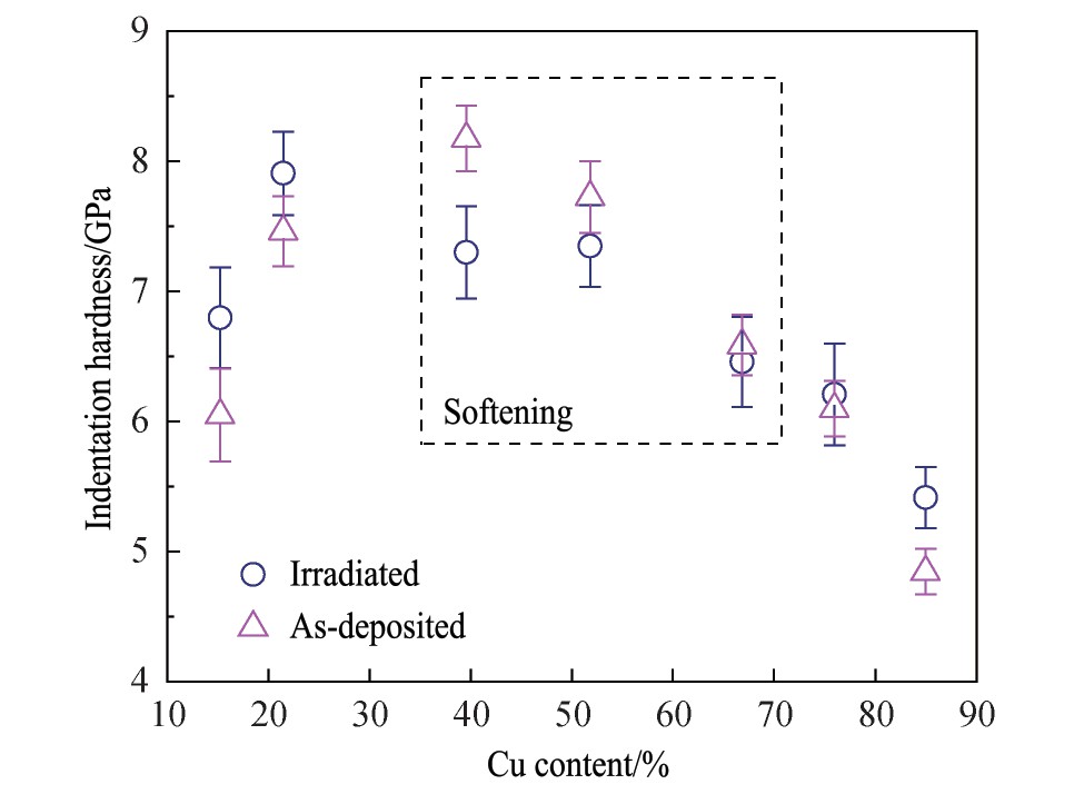
Understanding the microstructural response of metals and alloys to the radiation of particles,such as electrons,neutrons,protons and ions,is vital for the service extension of the existed nuclear materials and the development of new radiation-tolerant structural materials for the next generation nuclear energy. It has been shown for decades that the interfaces in metals and alloys are effective in capturing and sinking the radiation-induced point defects and defect clusters,leading to enhanced radiation tolerance. In this study,we have obtained abundant crystal/amorphous interfaces in Cu-Nb alloy thin films,which were later on subject to He ion irradiation. The microstructure and indentation hardness of the pristine and irradiated specimens have been studied and compared. Seven CuxNb100-x(x=15,25,35,50,65,75,85(%,atom fraction))thin film specimens were deposited on oxidized single crystal silicon(100)substrates using magnetron co-sputtering technique at room temperature. The as-deposited thin film specimens were irradiated by 100 keV He ions to the dose of 6��1020 m-2 at room temperature in a vacuum chamber. X-ray diffraction(XRD)results showed that the Cu-Nb thin films were composed of single crystalline phase when the Cu content was ��25% or ��75%,as indicated by the exclusive Cu or Nb peaks. Transmission electron microscopy(TEM)images revealed that the grains were equiaxed and the average grain size was about 100 nm. Nb-rich or Cu-rich regions were observed at the grain boundaries owing to the high intermixing enthalpy between Cu and Nb. When the Cu content ranged from 35% to 65%,the Cu-Nb thin films were composed of both crystalline and amorphous phases.The crystalline phase was in the form of particles,which embedded uniformly in the amorphous matrix. All of the dual phase specimens showed a wide peak between Cu(111)and Nb(110)in the XRD pattern. The wide peak moved towards Cu(111)with the increasing of Cu content and vice versa. After He irradiation,the He bubbles were observed to reside uniformly within the equiaxed grains of the single phase specimens,showing no preferential distribution. As for the dual phase specimens,the He bubbles however distributed primarily at the crystalline/amorphous interfaces. It was suggested that the preferential distribution of the He bubble might be related to the high energy state of crystalline/amorphous interfaces as well as the unlimited sinking effect of the amorphous phase.An additional possible reason was that the partial crystallization of the amorphous phase might have led to local volume contraction,giving rise to the negative pressure at the interfaces and hence the concentration of He atoms. It was noteworthy that we had not observed complete inhibition of the nucleation of the He bubbles,in contrast to the Cu-Nb multilayers. This is likely due to the bias absorption of interstitials and vacancies at the interfaces. Another possible explanation was that the interfaces density was not sufficiently high such that the critical concentration of He atoms could be reached and the He bubble nucleation occurred. Last,nanoindentation results showed that significant radiation induced hardening for Cu-Nb thin film specimens in which the Cu content was ��25% or ��75%.The indentation hardness of these specimens increased by 0.1��0.8 GPa after He ion irradiation. Such hardening behavior could be interpreted using the Taylor hardening model,i.e. the hardening originated from the pinning of dislocations by the He bubbles. In contrast,radiation induced softening was observed in specimens with Cu content ranging from 35% to 65%. This was possibly attributed to radiation induced crystallization,which decreased the volume fraction of the amorphous phase(the hard phase)and hence reduced the average hardness of the specimen.
Ϊ̽��������Ʒ�ķ������ˣ���������Ϊ100ke V��He���ӽ���ע��ʵ�顣ͼ3Ϊ����KinchPeach������SRIM����ģ����
[13]��������Ʒ��ԭ��ƽ����λ�ʣ�dpa,displacement per atom����HeŨ�ȶ��ߵķ�ֵ��Ⱦ�Ϊ300 nm���ң����´��ڱ�Ĥ��ȷ�����м�λ�ã�����Ҫ�����������˫�������TEM��Ʒ�е��Ա�����
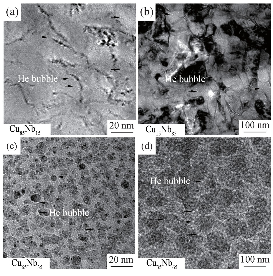
��He���ӷ��պ���Ʒ������ò��ͼ4��ʾ�����ڲ����ھ���/�Ǿ������Cu85Nb15��ͼ4(a������Cu15Nb85��ͼ4(b������Ʒ��He����Ҫ�ʾ�����ɢ�ֲ���δ��He���ھ��紦����ƫ�ۡ�ǰ��He���ܶȣ���λ���He��������ԼΪ8��1023m-3(TEM��Ʒ���ȡ100 nm��������He���ܶ�ԼΪ2��1022m-3�������Դ��Nbԭ����λ�ܣ�60 e V����������Cuԭ����λ�ܣ�30 e V)
[14]�����Nb�����ߵľ����н����γɵ�ȱ�ݡ������ں�����/�Ǿ������Cu65Nb35��ͼ4(c������Cu35Nb65��ͼ4(d������Ʒ��ƽ��He���ܶ�Ϊ4��1022��6��1022m-3������Cu85Nb15��Cu15Nb85��Ʒ֮�䡣He����Ҫ�ֲ��ھ���/�Ǿ����洦���������Ǿ����ڲ���He�����Էֱ棬��˵������/�Ǿ��������Heԭ���н�ǿ�������á��������Ƕȿ��ǣ�����/�Ǿ������Heԭ�ӵIJ�������Դ�������ṹ��ɵĸ���̬�����뾧��/���������������
[8]�����Ӷ���ѧģ������֤ʵ������Խ�ߵĽ��棨��߽Ǿ��磩��ȱ��ƽ���γ���һ��Խ�ͣ�����ζ��ȱ������Ǩ�������ܽ��洦
[7,8]������/�Ǿ����洦ԭ�ӵ���λ�����ھ���/������棬���ǰ�߽�������״̬���ܸ��ߣ��������ڲ���Heԭ�ӡ����ڽ϶�Heƫ���ڽ��洦������Զ����洦��Heԭ��Ũ�ȵ���He���κ��ٽ�ֵ
[15]�����ھ����Ǿ����ڲ��ټ�He�ݡ�Ӧ�ᵽ���ǣ��Ǿ�����������̬Ҳ�ϸߣ����������п���Ϊ�����ڵ�ȱ�ݣ�ȱ��He�ݵ��κ�λ�㣬��ʵ����δ�۲쵽He���ڷǾ����ڷֲ������⣬He���ھ���/�Ǿ�����ƫ�ۻ�����������յ��Ǿ��������йأ��������¾ֲ�����������ڷǾ��߽�����ɸ�ѹ��������He�ۼ����ٽ�He���ڽ��洦�κˡ�
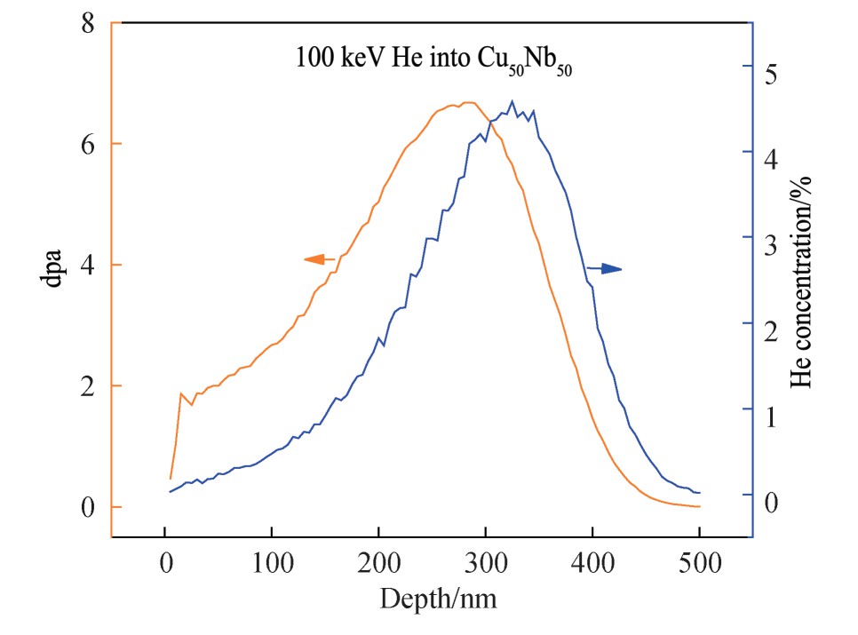
ͼ3 ����Ϊ100 ke V������Ϊ6��1020m-2��He���ӷ���Cu50Nb50�Ͻ��SRIMģ����
Fig.3 SRIM simulation results of Cu50Nb50irradiated by 100ke V He ions to the dose of 6��1020m-2