
Effects of temperature and pressure on morphologies of quasi-one-dimensional ZnO nanostructures fabricated via thermal evaporation
LIU Wen-cheng(���ij�), CAI Wei(�� ΰ), MENG Xiang-long(������)
School of Materials Science and Engineering, Harbin Institute of Technology, Harbin 150001, China
Received 10 April 2006; accepted 25 April 2006
Abstract��Quasi one-dimensional zinc oxide nanomaterials were synthesized by thermal evaporation. The structure, morphologies and composition of ZnO nanomaterials prepared under different conditions were studied by XRD, TEM, SEM and EDX. The morphologies are strongly sensitive to the temperature and the pressure during growth, including nanowires, nanobelts, nanocombs and pyramidal-like nanomaterials.
Key words: ZnO; nanomaterial; morphology; thermal evaporation
1 Introduction
Quasi-one-dimensional nanomaterials, such as nanowires [1, 2], nanobelts [3, 4] and nanotubes [5], have been successfully synthesized and have received much attention due to their fundamental properties. Quasi one dimensional nanostructures have great potential for testing and understanding fundamental concepts about the roles of dimensionality and size on physical properties and hold promise for a wide range of potential applications in nanodevices [6-8].
Tremendous attention has been paid to ZnO nanostructures because of novel physical properties and their potential applications in constructing nanoscale electronic and optoelectronic devices [9]. Among the methods used to fabricate ZnO nanostructures, the vapor deposition has been widely used due to low cost and simplicity. Morphology-controllable synthesis is very important to nanoscale science. The shape-controllable synthesis of ZnO nanorod arrays has been realized via the vapor phase growth method [10]. The parameters of temperature and pressure have important effects on the final morphology and structure of the product. The emphasis of this study was placed on the correlation of the temperature and pressure with the morphology of ZnO nanostructures.
2 Experimental
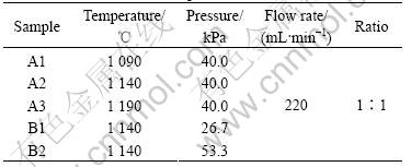
Fabrication of ZnO nanostructures was based on thermal evaporation process of ZnO power and active graphite without the presence of any catalyst. The synthesis process was carried out in a horizontal furnace with an alumina tube. The source material was highly pure ZnO powder mixed with active carbon (mole ratio is 1��1), which was placed in the alumina boat and then pushed into the center of the alumina tube with substrates at the down stream. Before heating, the tube was pumped, followed with the inert gas argon filling, and then repumped. This operation was repeated several times to eliminate O2. After that, the mixture was heated to certain temperature and maintained for 90 min and then cooled to room temperature with Ar gas which was controlled by a flow controller. White product was obtained on the substrate. To understand the effect of parameters on the morphologies, we performed the reaction at different temperatures and pressures. The parameters are listed in Table 1.
The morphologies and composition of the as-grown products were investigated using electron microscopy (SEM, HITACHI 4700) equipped with energy dispersive X-ray spectroscopy (EDS). The structure and phase purity of products were characterized by X-ray powder
Table 1 Different experimental parameters to fabricate ZnO nanostructure via thermal evaporation
diffraction (XRD) and transmission electron microscopy. Photoluminescence (PL) measurement was carried out at room temperature.
3 Results and discussion
Fig.1 shows the morphologies of the as-prepared products with different temperatures when the pressure is 40.0 kPa. It can be seen that the A1 samples are irregular nanowires with the diameter of several tens nanometers. The A2 samples are nanocombs and long wire-like nanowires with a typical length up to several tens of microns and a uniform diameter about 50-100 nm, which are shown in Fig.1(b). The magnified image of nanocomb is shown in Fig.1(c). The length of the nanocomb teeth is about 5 mm, the width is 20-100 nm, the width of the ridge is about 1��m and the thickness is several hundreds nanometers. In most comb-shaped nanostructures, the nanorods or nanobelts as the teeth were grown from one-side or both-sides of rod-shaped or belt-shaped spine of the ZnO nanocombs. The polarization of ZnO is thought to be an important effect for the formation of the comb-shaped ZnO nanostructure [11]. Fig.1(d) shows the ZnO nanostructure of the A3 samples with the pyramidal-like morphology.
Fig.2 shows the SEM images of the products with various pressures when the temperature is 1 140 ��. It is clearly seen that the pressure plays an important role in the morphologies of ZnO nanowires. The diameters of the nanowires increase from 50 to 200 nm while the pressure decreases from 53.3 kPa to 26.7 kPa.
A typical XRD pattern of ZnO nanostructure taken from the A2 samples is shown in Fig.3. The XRD pattern of the A2 samples can be indexed to a hexagonal wurtzite structure of ZnO. The positions of XRD peaks are in good agreement with those of the hexagonal structure of bulk ZnO with lattice constants of a=0.32 nm, c=0.52 nm which correspond to JCPDS Card [12].
The microstructure of the ZnO nanowires is further investigated by TEM observation. Fig.4(a) shows a typical TEM image of ZnO nanowires and nanobelts obtained from the A2 samples. An individual straight ZnO nanowire is shown in Fig.4(b) with a diameter about 150 nm. The nanowires are also characterized by selected-area-energy diffraction (SAED) as illustrated in the insert in Fig.4(b). The SAED pattern clearly shows that the nanowire is a single-crystal structure. No nanocomb is observed during the TEM observations. Maybe it was destroyed when the products were ultrasonically dispersed in ethanol.
Fig.5 shows the EDS analysis taken from the A2 samples, indicating that all the nanostructures have the
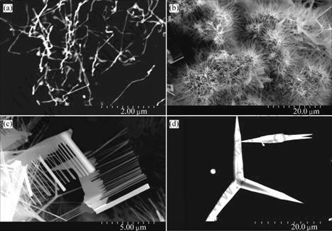
Fig.1 FE-SEM image of ZnO nanostructures: (a) Irregular ZnO nanowires synthesized at 1 090 ��; (b) ZnO nanocombs and nanowires synthesized at 1 140 ��; (c) High magnification image of ZnO nanocombs synthesized at 1 140 ��; (d) Pyramidal-like ZnO microstructures synthesized at 1 190 ��
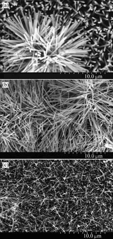
Fig.2 ZnO nanowires fabricated under different pressures: (a) 26.7 kPa; (b) 40.0 kPa; (c) 53.3 kPa
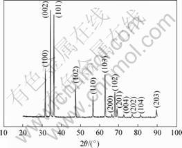
Fig.3 X-ray diffraction patterns of ZnO nanostuctures
same composition. Further quantitative analysis of EDS reveals that the mole ratio of Zn to O is about 58.91��41.09. There are many O vacancies in the quasi one dimensional ZnO nanostructures.
Fig.6 shows the PL spectrum of the A2 samples at room temperature. A low-intensity broad UV peak at 380 nm wavelength and a high-intensity green peak at 520 nm wavelength are observed from the curve. The UV
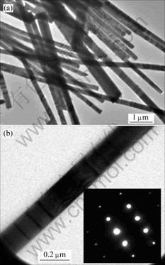
Fig.4 TEM images of ZnO nanostructures: (a) Low magnification; (b) High magnification (The insert is the SAED pattern of ZnO nanowire.)
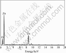
Fig.5 EDS spectrum of A2 samples
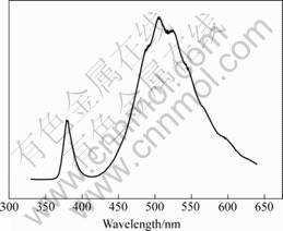
Fig.6 PL spectrum of products at room temperature
emission corresponds to the near band-edge (NBE) emission, namely the recombination of free excitons through an exciton-exciton collision process. The green transition is referred to a deep-level or trapped-state emission which is attributed to the green transition of the single ionized oxygen vacancy in ZnO. The high- intensity of the green luminescence corresponds to high quantity of the surface oxygen vacancies which can be controlled through heat treatment [13].
Most of ZnO nanowires were synthesized through vapor-liquid-solid (VLS) growth mechanism using a catalyst and there was a little particle at the end of the nanowires [14,15]. In the present work, no metal catalyst was used and no particle was observed at the end of the nanostructures. Therefore, the growth mechanism of the products can be understood on the basis of a self-catalytic process with the vapor-solid (VS) growth mechanism [3]. During heating, active carbon reduced ZnO into Zn and then Zn vapor or droplets were transferred to the low temperature area to be oxidized forming ZnO nanostructures. The oxygen in the ZnO has originally come from the air leakage or the residual oxygen of the furnace. The morphologies are sensitive to the furnace temperature because the evaporation rate and the nucleation rate are strongly influenced by the temperature. The temperature provides energy for zinc particles to vaporize. When the temperature is too high (1 190 ��), the temperature of the substrates is too high to deposition products and the critical size for nucleation is large. As a result, the pyramidal-like ZnO nanostructure is obtained at a relatively high temperature. Whereas when the temperature is low, the decrease of the Zn vapor concentration leads to the formation of the irregular nanowires. The regular ZnO nanostructures can only be obtained with a proper growth temperature (1 140 ��).
The pressure also has an obvious effect on the morphologies of ZnO nanostructures. As mentioned above, the diameter of the ZnO nanostructure decreases with increasing pressure. In higher pressure, less Zn vapor was evaporated at the position of the source materials due to the presence of inert gas. In this case, the surface of source materials was surrounded by a thin vapor layer through which the atoms or molecules evaporating from the source materials would diffuse. Once the atoms or molecules reached the outer boundary of the layer, they could be carried away or redeposited on the source materials due to collisions with the inert gas, thus leading to a reduced evaporation rate as compared with that at lower pressure. Consequently the density of Zn vapor surrounding the nanowires at cold finger is lower and the nanowires are thinner in the higher pressure than that in the lower pressure. This can be explained that the high pressure depresses the diffusion of the reactant and the growth kinetics. When the pressure is high, the oxygen and the zinc partial pressure in the reaction chamber is high and then the nucleation rate is high, so the diameter is thinner than that of the nanowires under lower pressure, and the nucleation rate also has a great impact on the diameter of the products.
4 Conclusions
Quasi-one-dimensional ZnO nanostructures have been synthesized successfully on silicon substrate via the thermal evaporation. The products exhibit nanowires, nanorods, and nanocombs, pyramida-like microstructure, which are very sensitive to the positions relative to the temperature and the pressure and can be controlled by adjusting the growth parameters. The results show that the regular ZnO nanowires and nanocombs are deposited at the temperature of 1 140 �� and the pressure of 26.7 kPa.
Reference
[1] CHEN Y Q, CUI X F, ZHANG K, et al. Bulk-quantity synthesis and self-catalytic VLS growth of SnO2 nanowires by lower-temperature evaporation [J].Chem Phys Lett, 2003, 369: 16-20.
[2] ZHANG HZ , YU DP, DING Y, et al. Dependence of the silicon nanowire diameter on ambient pressure [J]. Appl Phys Lett, 1998, 73: 3396.
[3] PAN Z W, DAI Z R, WANG Z L. Nanobelts of semiconducting oxides [J]. Science, 2001, 291: 1947-1949.
[4] COMINI E, FAGLIA G, SBERVEGLIERI G, PAN Z W, WANG Z L. Stable and highly sensitive gas sensors based on semiconducting oxide nanobelts [J]. Appl Phys Lett, 2002, 81: 1869-1871.
[5] AJAYAN P M, IIJIMA S. Capiliarity-induced filling of carbon nanotubes [J]. Nature, 1993, 361: 333.
[6] KOUKLIN N, MENON L, WONG A Z, et al. Giant photoresistivity and optically controlled switching in self-assembled nanowires [J] . Appl Phys Lett, 2001, 79: 4423-4425.
[7] HUANG Y, DUAN X F, CUI Y, et al. Logic gates and computation from assembled nanowire building blocks [J]. Science, 2001, 294: 1313-131.
[8] BACHTOLD A, HADLERY P, NAKANISHI T, DEKKER C. Logic circuits with carbon nanotube transistors [J]. Science, 2001, 294: 1317-1320.
[9] BOWER C, ZHOU Q, ZHU W, et al. Nucleation and growth of carbon nanotubes by microwave plasma chemical vapor deposition [J]. Appl.Phys Lett, 2000, 77: 2767-2769.
[10] SUN X C, ZHANG H Z, XU J, et al. Shape controllable synthesis of ZnO nanorod arrays via vapor phase growth[J]. Solid State Commun, 2004, 129: 803-807.
[11] MOORE D, RONNING C, MA C, WANG Z L. Wurtzite ZnS nanosaws produced by polar surfaces[J]. Chem Phys Lett, 2004, 385: 8-11.
[12] JCPDS Card No.36-1451.
[13] LU H Y, CHU S Y, CHENG S H. The vibration and photoluminescence properties of one-dimensional ZnO nanowires[J]. J Cryst Growth, 2005, 274: 506-511.
[14] LI S Y, LEE C Y, TSENG T Y. Copper-catalyzed ZnO nanowires on silicon (100) grown by vapor�Cliquid�Csolid process[J]. J Cryst Growth, 2003, 247: 357-362.
[15] LIANG C H, CHEN L C, HWANG J S, et al. Selective-area growth of indium nitride nanowires on gold-patterned Si(100) substrates [J]. Appl Phys Lett, 2002, 81: 22-24.
(Edited by PENG Chao-qun)
Corresponding author: CAI Wei; Tel: +86-451-86412505; Fax:+86-451-86413922; E-mail: liuwc@hit.edu.cn, weicai@hit.edu.cn