
Numerical simulation of thermal-mechanical process of Al-Si-Pb alloy treated by high current pulsed electron beam
L? Xiao-xia(吕晓霞), LI Rong-guang(李荣广), AN Jian(安 健)
Key Laboratory of Automobile Materials, Ministry of Education, Jilin University, Changchun 130025, China
Received 28 July 2006; accepted 15 September 2006
Abstract: The modified microstructure of Al-Si-Pb alloys irradiated by high current electron beam (HCPEB) reveals three distinct regions: a molten zone, an overlapped zone of heat-affected and quasistatic thermal stress-affected zone, and a transition zone followed by the substrate. The hardness and wear properties of the alloys were significantly improved. To better understand these changes in microstructure and properties, the physical model for the simulation of temperature and quasistatic stress fields was established. Based on experimental investigation and physical models, the temperature field and stress field were simulated for Al-Si-Pb alloy. The starting melting position, largest crater depth, melting layer thickness, and quasistatic stress distribution were obtained. These results reveal the mechanism of crater formation on the surface and improvement of hardness and wear resistance.
Key words: Al-Si-Pb alloy; high current pulsed electron beam; numerical simulation; crater; quasistatic stress
1 Introduction
The liquid immiscible alloys based on Al-Pb system are potential materials for application in automobile industry. The metallurgical problems, the segregation arising from liquid immiscibility in a wide range of temperature and composition and also large density difference of the constituent phase, have been overcome by employing several unconventional techniques including rapid solidification, stircast, spray forming, powder metallurgy and mechanical alloying [1-4]. To further improve the wear properties of this kind of bearing material, more studies focus on the composites containing submicron or nanoscaled particles of soft lead synthesized by nonequilibrium processing for tribological application [5-6]. Recent publications indicated considerable efforts in processing nanoscaled dispersoids of lead in aluminum alloys by rapid solidification and understanding the influence of these nanoscaled particles on tribological properties [7-8]. The refinement of Pb phase is found to greatly improve the wear properties of Al-Pb alloys.
Proper surface modification techniques can effectively refine the microstructure of materials surfaces, hence the properties were improved. Among them, high current pulsed electron beams (HCPEB) is particularly advantageous due to extremely high instantaneous energy density, short irradiation time, and high surface finishing without any change in the substrate materials. The instantaneous energy deposition induces rapid solidification, evaporation, thermal stress, shocking wave, and enhanced diffusion [9-10]. This technique has demonstrated significant improvement of wear resistance of various steel materials. However, reports on the effect of surface modification of nonferrous metals by HCPEB, especially light alloys such as Al-Pb alloys that contain particles with low melting temperature, are rare and more efforts should be made to gain a better understanding of the microstructure evolution involved. In this study, we focus on the thermal-mechanical effects induced by high current pulsed electron beam treatment on the microstructure evolution involved based on physical model for the temperature and quasistatic stress fields.
2 Experimental
The composition of the alloy was Al-4%Si-25%Pb- 1.0%Cu-0.5%Mg-0.4%Mn-1.0%Sn(mass fraction). Al- Si-Pb alloys were fabricated by using stircasting, the cylindrical ingots were extruded into strips and then were cut into dimension of 15 mm×15 mm×1.2 mm.
The pulsed electron beam treatment was conducted on a Nadezhda-2 type HCPEB source. More details about the HCPEB system can refer to PROSKUROVSKY et al [11]. The HCPEB parameters used to treat the samples were as follows: energy density Es=1.5-2.5 J/cm2; pulse duration 1.5 μs; number of pulses N=15. Specimens were prepared from the HCPEB treated material for cross-sectional microstructure investigation and hardness measurement using standard grinding and polishing procedures, the sizes and distribution of lead and silicon particles were subsequently estimated using EPMA and SEM. The melting zone microstructure characterization was carried out using H-800 transmission electron microscope (TEM) operated at 200 kV.
3 Results and numerical simulation of thermal-mechanical process
3.1 Microstructure and properties
Fig.1(a) shows the surface morphology of HCPEB treated sample. Craters are observed, typically 4.5-7.0 μm in width, and with decreasing electron energy their width decreases. The SEM cross-sectional image of HCPEB treated sample is shown in Fig.1(b). Fig.1(b) shows the occurrence of three distinct regions, i.e. a molten zone, an overlapped zone of heat-affected and quasistatic thermal stress-affected zone, and a transition zone followed by the substrate. The melting zone has a depth of about 4.0 μm and the overlapped zone has a depth of about 33.3 μm. After HCPEB irradiation, the microstructure changes considerably, especially the shape of lead undergoes a change from continuous wide strip-shape to discontinuous thin grain shape and its size decreases considerably.
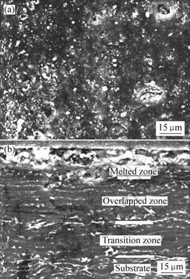
Fig.1 SEM images of Al-Si-Pb alloy surface (a) and cross section (b) irradiated by HCPEB with 2.5 J/cm2
The great difference in microstructures induced by HCPEB irradiation suggests a corresponding improve- ment in mechanical properties. This can be seen in Figs.2 and 3. The hardness and wear resistance are improved considerably.
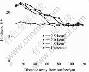
Fig.2 Microhardness profiles of Al-Si-Pb alloy HCPEB irradiated with various energy densities
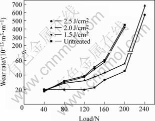
Fig.3 Variation in wear rate with load for untreated and irradiated Al-Si-Pb alloys
3.2 Physical model for simulation of temperature and quasistatic stress fields
During the HCPEB processing, the target absorbs about 90% beam energy, as a result, a nonstationary temperature is generated in the surface layer, which in turn induces a coupled dynamic stress field. There exist two kinds of stress fields induced by the bombardment, a quasistatic thermal stress and a dynamic thermal stress. From the theory of thermal-elasticity, it is known that the quasistatic stress is caused by a temperature gradient in the direction of the thickness, while the dynamic stress is a kind of inertia force associated with super-fast thermal expansion of the solid, which is quite small and is negligible. The power absorption per unit volume can be expressed as
 (1)
(1)
where ηA is the absorption rate of the impinging beam power, U is the accelerating voltage, j(t) is the electron current density, P(t) is the power of electron beam, S is the irradiation area of the electron beam, and f(x, r) is the distribution function of the absorbed power density over the electron range in the target which can be described by
 (2)
(2)
as well as r(t) is the electron range in the target calculated from the formula
 (
( ) (3)
) (3)
The temperature field T (x, t) can be calculated by solving a one-dimensional thermal conductivity equation
 (4)
(4)
Under the initial condition:
T(x, 0)=T0 (5)
The boundary condition:
 , Tn=293 K (6)
where r is the mass density, c(T) is the specific heat capacity, k(T) is the thermal conductivity, L is the latent heat per unit mass, J/kg. The thermal conductivity k and specific heat capacity c are intrinsic properties of the material and the functions of the temperature T. In our numerical simulation, we adopt the equivalent heat quantity method i.e. the absorbed and released latent heats per unit volume are converted into temperature compensation.
From the theory of thermal-elasticity, the quasistatic thermal stress of a plate subject to a temperature distribution T(x, t) through the thickness is described by
 (7)
(7)
where μ is the Poisson’s ratio, a is the thermal expansion coefficient, E is the elastic modulus, NT is a resultant force, MT is the bending moment.
 (8)
(8)
 (9)
(9)
3.3 Numerical simulation
Numerical simulations were carried out on the basis of Al-Pb and Al-Si binary phase diagrams. Fig.4 shows the temperature distribution of Al-Si-Pb alloy over a depth range of 0-40 μm and a time range of 0-2 μs. The flat area of the profile is the melting plateau of Al-Si eutectic at 578 ℃, above it is the liquid-solid two-phase region. Fig.5 presents the contour plots of the compensation temperature versus depth and time. It can be seen that the complete melting in Al-Si-Pb above 620 ℃ starts from 0.56 μs at about 1.05 μm in depth. At this time, the outer surface is still in solid state, and at 0.61μs the outer surface melts completely. The liquidized sublayer, confined by the outer solid layer, tends to erupt through the surface, and to create the craters. The melting depth reaches 1.65μm, which is the maximum depth of the craters. The maximum melting depth occurs at 4.4 μm at 1.2 μs. This result agrees with the observed melted zone depth of about 4.0 μm.

Fig.4 Temperature field of irradiated Al-Si-Pb at 2.5 J/cm2
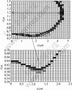
Fig.5 Contour plot of compensation temperature of alloy Al-Si-Pb arising from heat of melting
Fig.6 shows the evolution of the quasistatic thermal stress in irradiated Al-Si-Pb alloy at 1.5 J/cm2. It can be seen that the compress stress and tensile stress operate in a range of 60 μm near the surface, and compress stress at depth of 8 μm is so high that it exceeds the yield strength of Al-Si-Pb alloy, and induces the work-hardening effect. The structural evolution and hardness increase account for the improvement of wear resistance of Al-Si-Pb alloy by HCPEB treatment.
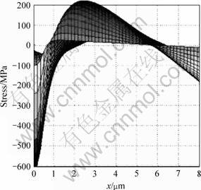
Fig.6 Side view of quasistatic stress in Al-Si-Pb alloy at 1.5 J/cm2
4 Conclusions
1) After high current pulsed electron beam irradiation of Al-Pb alloy, three distinct zones are formed sequentially near the surface, improving considerably the alloy’s microstructure and hardness.
2) Physical models have been established and numerical simulations have been performed to describe the structural evolution and associated thermal mechanical effects induced by HCPEB treatment.
References
[1] PATHAK J P, TIWARI S N, MALHOTRA S L. Microstructure and mechanical properties of leaded aluminum alloy [J]. Met Technol, 1983, 10: 413-419.
[2] HOWE D P, MEE M, TORRANCE A A, WILLIAMS J P. Al-Pb-Si-In bearing alloy [J]. Mater Sci Technol, 1991, 7: 330-333.
[3] ZHAO J Z, DREES S, RATKE L. Strip casting of Al-Pb alloys―A numerical analysis [J]. Mater Sci Eng A, 2000, 282: 262-269.
[4] ZHU M, GAO Y, CHUNG C Y. Improvement of the wear behavior of Al-Pb alloys by mechanical alloying [J]. Wear, 2000: 47-53.
[5] AN J, DONG C, ZHANG Q Y. Improvement of wear behavior of stircast Al-Si-Pb alloys by hot extrusion [J]. Tribol Int, 2005, 36: 25-34.
[6] RAJULAPATI K V, SCATTERGOOD R O, MURTY K L. Effect of Pb on the mechanical properties of nanocrystalline Al [J]. Scripta Mater, 2006, 55: 155-158.
[7] BHATTACHARYA V, CHATTOPADHYAY K. Microstructure and wear behavior of aluminum alloy containing embedded lead dispersolids [J]. Acta Mater, 2004, 52: 2293-2304.
[8] GABRISCH H, KJELDGAAD L, JOHNSON E, DAHMEN U. Equilibrium shape and interface roughening of small liquid Pb inclusions in solid Al [J]. Acta Mater, 2001, 49: 4259-4269.
[9] GUAN Q F, ZHANG Q Y, DONG C. Deformation twining in single-crystal aluminum induced by high-current pulsed electron beam [J]. J Mater Sci, 2005, 40: 5049-5052.
[10] DONG C, WU A, HAO S, ZOU J, LIU Z, ZHONG P. Surface treatment by high current pulsed electron beam [J]. Surf Coat Technol, 2003, 163: 620-624.
[11] PROSKUROVSKY D I, ROTSHTEIN V P, OZUR G E, IVANOV Y F, MARKOV A B. Physical foundations for surface treatment of materials with low energy, high current electron beams [J]. Surf Coat Technol, 2000, 125: 49-56.
(Edited by LONG Huai-zhong)
Foundation item: Project(50375063) supported by the National Natural Science Foundation of China
Corresponding author: AN Jian; Tel: +86-431-5095874; E-mail: anjian@jlu.edu.cn