AC measurements of spray-deposited CdS:In thin films
��Դ�ڿ������ϴ�ѧѧ��(Ӣ�İ�)2012���3��
�������ߣ�S. J. Ikhmayies R. N. Ahmad-Bitar
����ҳ�룺829 - 834
Key words��II-VI compounds; spray pyrolysis; impedance; dielectric loss; Bode plots
Abstract:
Indium doped cadmium sulfide thin films (CdS:In) were produced by the spray pyrolysis technique on glass substrates. AC measurements were used to investigate the electrical properties of the films depending on Brick-layer model for polycrystalline materials. The measurements were performed at room temperature in the dark and room light in the frequency range from 20 Hz to 1 MHz using coplanar indium electrodes. The data were analyzed by using Bode plots for the impedance Z and dielectric loss tan�� with frequency f. It is found that the impedance has no dependence on frequency in the low frequency region but has 1/f dependence in the high frequency region. One dielectric loss peak is obtained, which means the presence of a single relaxation time, and hence the films are modeled by just one RC circuit which represents the grains. This means that there is just one conduction mechanism that is responsible for the conduction in the bulk, due to electronic transport through the grains. Real values of the impedance in the low frequency region and relaxation times for treated and as-deposited films were estimated.
J. Cent. South Univ. (2012) 19: 829-834
DOI: 10.1007/s11771-012-1079-1![]()
S. J. Ikhmayies1, R. N. Ahmad-Bitar2
1. Department of Basic Sciences-Physics, Faculty of Information Technology, Al Isra University,Amman 16197, Jordan;
2. Physics Department, Faculty of Science, University of Jordan, Amman 11942, Jordan
? Central South University Press and Springer-Verlag Berlin Heidelberg 2012
Abstract: Indium doped cadmium sulfide thin films (CdS:In) were produced by the spray pyrolysis technique on glass substrates. AC measurements were used to investigate the electrical properties of the films depending on Brick-layer model for polycrystalline materials. The measurements were performed at room temperature in the dark and room light in the frequency range from 20 Hz to 1 MHz using coplanar indium electrodes. The data were analyzed by using Bode plots for the impedance Z and dielectric loss tan�� with frequency f. It is found that the impedance has no dependence on frequency in the low frequency region but has 1/f dependence in the high frequency region. One dielectric loss peak is obtained, which means the presence of a single relaxation time, and hence the films are modeled by just one RC circuit which represents the grains. This means that there is just one conduction mechanism that is responsible for the conduction in the bulk, due to electronic transport through the grains. Real values of the impedance in the low frequency region and relaxation times for treated and as-deposited films were estimated.
Key words: II-VI compounds; spray pyrolysis; impedance; dielectric loss; Bode plots
1 Introduction
Cadmium sulfide (CdS) is a brilliant II�CVI semiconductor material with a direct bandgap of 2.42 eV at room temperature [1]. It has many promising applications in multiple technical fields including photochemical catalysis, gas sensors, detectors for laser and infrared, solar cells, nonlinear optical materials, various luminescence devices, optoelectronic devices and so on [1]. There are different methods to prepare undoped and doped CdS films, such as rf sputtering [2] chemical bath deposition (CBD) [3], pulsed laser deposition (PLD) [4], and spray pyrolysis (SP) [5-11]. Of these methods, the spray pyrolysis represents the less expensive alternative, and can produce large area high-quality low-cost thin films [12].
The electrical properties of CdS films, as II�CVI semiconductors, are of considerable interest because of their potential use in the fabrication of solar cells. We previously studied the electrical properties of as-deposited and treated CdS:In thin films by using I-V plots and discussed them in the light of structural and optical properties [5-7, 9]. But because AC measurements have been extensively used to understand the conduction processes for different materials, we used them in this work to understand the conduction processes in CdS:In thin films. According to our knowledge, only few results are available in the literature regarding the AC measurements and dielectric properties of CdS. RAZA KHAN et al [1] studied optical and dielectric properties of CdS nanoparticles prepared by chemical synthesis. EL-BARRY and ATYIA [13] studied the dielectric relaxation and AC conductivity of CdS and ZnS compounds in bulk form. RINC?N et al [14] compared the optical, structural and photoelectron- chemical properties of nanocrystalline and polycrystalline CdS/ZnS thin films where impedance spectroscopy was used. ORTU?O-L?PEZ et al [15] investigated the impedance spectroscopy of chemically deposited CdS and PbS polycrystalline films.
The purpose of this work is to study the electrical properties of spray-deposited CdS:In thin films before and after treatments by using AC measurements, and to understand the conduction mechanisms depending on Brick-layer model for polycrystalline materials. The measurements were recorded at room temperature in the dark and room light before and after chemical and heat treatments in a wide frequency range (20 Hz-1 MHz). Impedance and loss angle measurements were analyzed and discussed by using Bode plots.
2 Experimental
The precursor solution of CdS thin films was prepared by dissolving 2.06��10-2 mol of extra pure
CdCl2��H2O (MERCK Art. 2011) and 2.24��10-2 mol of thiourea (NH2)2CS (>97% S) in 350 mL of distilled water. Indium chloride InCl3 (MERCK Art. 12471) was used as a doping compound. The ratio of the concentration of indium ions to that of cadmium ions in the solution which is not necessarily the same as their ratio in the films was 1.0��10-4 which is considered as the doping ratio. The solution was sprayed intermittently by using the spraying system described in Ref. [5] on glass substrates that were ultrasonically cleaned with methanol at a substrate temperature of 490 ��C. Some of the films were etched by a solution of HCl (about 36% HCl) in distilled water (1:100 by volume). The films were dipped in this solution for about 20 s, rinsed in distilled water and dried by an air drier. Two other sets of films were annealed at 400 ��C in nitrogen atmosphere by the annealing system described in Ref. [5]; one of them was annealed without HCl-etching and the other after HCl-etching.
AC measurements were performed with HP LCR meter 4284A spanning the frequency range from 20 Hz to 1 MHz. The thickness of film was estimated by using Lambert law for absorption in a semiconductor which is applicable at wavelengths lower than the cut-off wavelength. The linearity of the relation between ln(T/T0), where T/T0 is the relative transmittance measured by using a double beam Shimadzu UV 1601 (PC) spectrophotometer with respect to a piece of glass of the same kind as the substrates in the wavelength range of 300-1 100 nm, against thickness means that Lambert law is valid. We made this plot for CdS films of known thickness prepared by vacuum evaporation at three different values of wavelength that are lower than the cut-off value: 420, 435 and 450 nm. The best linear fit was obtained for the wavelength ��=435 nm. We took the absorption coefficient from Ref. [4] at this wavelength which is about 1.1��105 cm-1 for the undoped CdS thin films. This value of the absorption coefficient can be used for our films because they are lightly doped (1.0��10-4). This estimation results in an uncertainty in the film thickness of about �� 3 nm. The produced films have thickness of about 100-150 nm.
3 Results and discussion
Brick-layer model assumes that the polycrystalline material is a three-dimensional network of cubic shaped crystallites of size D with resistivity ��g and capacitance Cg, separated by the grain boundaries having width d, resistivity ��gb and capacitance Cgb. Each component of the polycrystalline material can be represented by an RC circuit, and the model assumes that the two circuits are connected in series. R and C are the electrical resistance and capacitance of each component in the corresponding circuit [15]. Figure 1 shows the equivalent circuit used to simulate the electrical response of the polycrystalline thin films, assuming the Brick-layer model. The circuit consists of two RC circuits and the resistance Rs, and all three are connected in series. The RgCg circuit is associated with the grains and the RgbCgb with the grain boundaries. The resistance Rs has been associated with the resistance of the contacts.
The impedance for a parallel RC network is always given by
![]() (1)
(1)
where ZR is the real part and ZI is the imaginary part, ![]() .
.
ZR and ZI are given by
![]() (2)
(2)
![]() (3)
(3)
where ��=2��f, is the angular frequency of the applied alternating electric field, and ��=RPCP is the relaxation time. The phase angle f is defined as tanf =ZI/ZR and it is related with the loss angle �� by the relation f+��=90��.
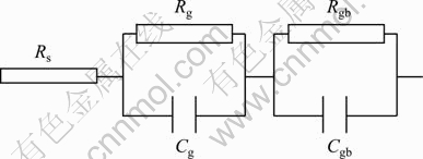
Fig. 1 Equivalent circuit best producing frequency response for polycrystalline films (Cg, Cgb, Rg, Rgb are correspondingly capacitance and resistance of grain and grain boundaries; Rs is resistance of contacts)
By applying Brick-layer model on our spray-deposited CdS:In thin films, it is found that Rs will be omitted from Fig. 1, because the contacts which are coplaner indium strips are ohmic [16], and the RgbCgb circuit related to grain boundaries will be omitted too, because just one relaxation time is found. So, the films will be modeled by the RgCg circuit which is related to the grains. This means that the grain boundaries have no contribution in the charge conduction, and the majority of the charge carriers responsible for the bulk conductivity are electrons through the grains. Bode plots were used to study the relations between ZR, ZI, Z, f, tan�� and the frequency.
Figure 2 displays the relation between the real part of the impedance ZR and the logarithm of the frequency. In Fig. 2(a), the relation is shown for one of the films in the dark and in room light. The difference between the behaviors in the two cases is apparent where the dark resistance in the low frequency region is large and we couldn��t measure it. The response to light has a significant decrease in ZR for f��6 kHz or lgf��3.78. For f>6 kHz the dark values of ZR become smaller than the values obtained in room light. No dependence of the light resistance ZR appears on frequency for f<10 kHz. Figure 2(b) shows the measurements in room light for the as-deposited and treated films for comparison. For the as-deposited and etched films, ZR is independent on frequency for f��1 kHz, and they have approximately the same values in the low frequency region. For the annealed films (with and without etching), ZR is independent on frequency for f��3.5 kHz or lgf��3.54 and it is smaller in the same frequency range than as-deposited and etched films. The estimated values of ZR in the low frequency region are listed in Table 1.
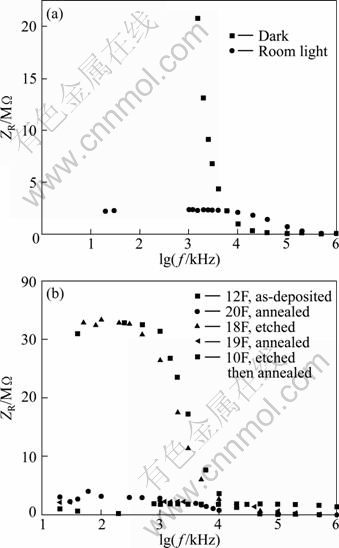
Fig. 2 Plots of real part of impedance against logarithm of frequency: (a) Film in dark and in room light; (b) A set of treated films in room light beside an untreated one
To explore the frequency dependence of the impedance, the relation between the logarithm of the total impedance Z and the logarithm of the frequency is represented in Fig. 3. Figure 3(a) displays this relation for a film in the dark and in the room light. From this figure, the 1/f dependence of the impedance in the high frequency range is apparent. A linear fit is performed in the linear regions and the slopes are found to be -0.98 and -0.93 for the dark and light curves, respectively. This result is consistent with that obtained by EL-BARRY and ATYIA [13] from the AC conductivity analysis.
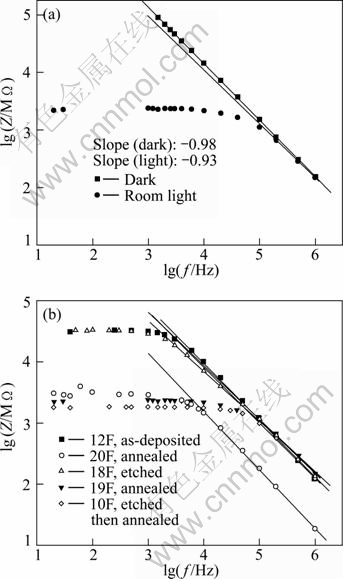
Fig. 3 Logarithm of impedance against logarithm of frequency: (a) Film in dark and room light; (b) As-deposited and treated films in room light
Table 1 Values of ZR in low frequency region, bending frequency fc, slopes from linear fit in Fig. 3, frequencies at ZI maximum fmax and relaxation time �� in room light

Figure 3(b) displays the same relation in room light for the as-deposited and treated films. Also in this case, the 1/f dependence of the impedance in the high frequency range is apparent and linear fits are performed in the linear regions. The slopes are found to be restricted in the range from -0.82 to -0.96 which are close to -1. The bending or onset frequency is not the same for the different films, which means that different relaxation times are found. The smallest bending frequency fc is about 1 kHz for the as-deposited and etched films, and the largest one is about 100 kHz for the annealed films and the etched then annealed film. The other annealed film shows a bending frequency of about 10 kHz. The different values of fc for the two annealed films are due to the difference in film thickness. The estimated slopes and bending frequencies fc for as-deposited and treated films are listed in Table 1.
Figure 4 shows the logarithm of the imaginary part of the impedance ZI against the frequency. The frequency at the maximum ZI (dielectric loss peak) is used to evaluate the relaxation time �� from the relation [13]:
![]() (4)
(4)
Figure 4(a) depicts the relation for a film in the dark and room light. The value of ZI in the dark has maximum at f=5 kHz, which means that the relaxation time is ��=31.8 ��s. The dark impedance in Fig. 4(a) is compared with its counterpart for polycrystalline and nanocrystalline screen-printed CdS thin films given in Ref. [14]. Both our and their curves show linearity, but the linearity in our curve extends from 1 kHz to 1 MHz and in Ref. [14] it is restricted in the range from 0.1 to less than 1 kHz. We notice that our curve does not show the slow decrease in the high frequency region, but their curve shows a slow decrease and then no dependence on frequency (lgZ=2) for f>1 kHz. The behavior of our curve is closer to the behavior of the nanocrystalline CdS film in Ref. [14], where no such constancy of Z is observed. The large value of impedance at low frequencies indicates that the film has a high capacitive behavior. If we compare our results with the results obtained by EL-BARRY and ATYIA [13] for the AC conductivity, we find that the onset frequency (bending frequency) that they got is fc=5 kHz but in our work it is just observed under illumination and it is about 10 kHz. The reason is that our films are polycrystalline but their results are for crystalline CdS in bulk form.
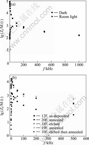
Fig. 4 Logarithm of imaginary part of impedance ZI against frequency: (a) For film in dark and room light; (b) For as-deposited and treated films in room light
Figure 4(b) shows the same relation for the as-deposited and treated films in room light. In all cases, there is a maximum but its position differs from one case to another. The values of the loss peak frequency fmax and the deduced relaxation time are listed in Table 1. Note that fc and fmax must be the same, but the estimation of fmax is more accurate than that of fc. The presence of one relaxation time means that there is electric transport mechanism in the films through the grains, and hence the equivalent circuit to our films is just one RC circuit, that is RgCg in Fig. 1 according to Brick-layer model. Since our contacts are indium coplaner strips, there is no contact resistance and Rs is also zero.
EL-BARRY and ATYIA [13] found that fmax=2.86 kHz for CdS in bulk form at T=303 K from which the relaxation time is �ӡ�55.7 ��s. By comparing this with our values shown in Table 1, we find that it is close to the values obtained for the as-deposited film in room light which is 53.1 ��s. The relaxation time is increased after etching and becomes 79.6 ��s, but it is strongly decreased after annealing and becomes 1.6 ��s for one film and 15.9 ��s for the other film. A large decrease has occurred after etching followed by annealing where it becomes 3.2 ��s. The explanation of this decrease in relaxation time is that annealing removes some defects or deep states and etching followed by annealing removes more defects as found in the analysis of the PL spectra of such films [8].
Figure 5 depicts the relation between the phase angle f and the frequency. In Fig. 5(a), this relation is shown for a film in the dark and room light. The large value of the phase angle indicates that the film is highly capacitive. The response to light is evident, where the phase angle has decreased in the whole frequency range. As Fig. 5 shows, for film in the light and dark, the phase angle is frequency independent until about 1 kHz, then it increases sharply with frequency. For the situation in the dark, it jumps to about 84.8�� at about 1 kHz, and for the situation in the light it becomes approximately 80�� at about 1 kHz. This behavior is expected because in the low frequency range the film behaves as a pure resistance Z��R and the phase f��0 and in the high frequency range the film behaves as a capacitor Z��1/��C and f��90��. Comparing the curve of the dark with those in Ref. [14], we find that it is closer to the one that represents nanocrystalline CdS thin films, but we have faster increase of the phase angle with frequency which is clear at f=1 kHz and they have gradual increase with frequency.
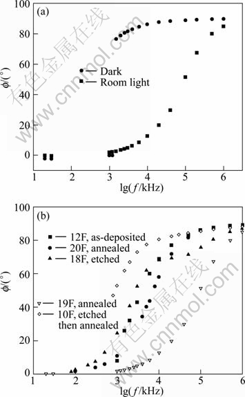
Fig. 5 Relation between phase angle and logarithm of frequency: (a) For film in dark and room light; (b) For as-deposited and treated films in room light (values of phase are negative but for simplicity sign is removed)
Figure 6 displays the relation between the dielectric loss (tan��) and the logarithm of the frequency. Figure 6(a) shows this relation for a film in the dark. A very small dielectric loss in the dark for all frequencies is observed. The largest value is 0.24 at the lowest frequency (f=40 Hz) and then it decreases to zero at higher frequencies. Comparing our graph with that obtained by RAZA KHAN et al [1] for CdS nanoparticles prepared by chemical synthesis, we find the same behavior but we have lower values of dielectric loss at all frequencies. The reason may be that our films are indium doped but their films are not doped. But if we compare our results with those obtained by EL-BARRY and ATYIA [13], we find that the value of dielectric loss of CdS:In thin films in the dark is found to be close to its value for the bulk CdS in the low frequency region which is in the range of 0-0.2 as obtained by these authors. But they got a maximum for bulk CdS which varies with temperature and our curves show a continuous decrease with frequency without such maximum. The peak in the loss tangent at a given frequency indicates the characteristic feature of a Debye-type relaxation process.
Figure 6(b) shows the same relation for the same film in dark and room light for comparison. The response to light has a large increase in the dielectric loss for all frequencies, but with the same behavior with frequency. Figure 6(c) shows the same relation for the as-deposited and treated films in room light. It is found that annealing has increased tan��, etching decreases it and etching followed by annealing decreases it more. For all samples, the dielectric loss decreases with frequency, and the same behavior is observed for treated and as-deposited films and it approaches zero at high frequencies.
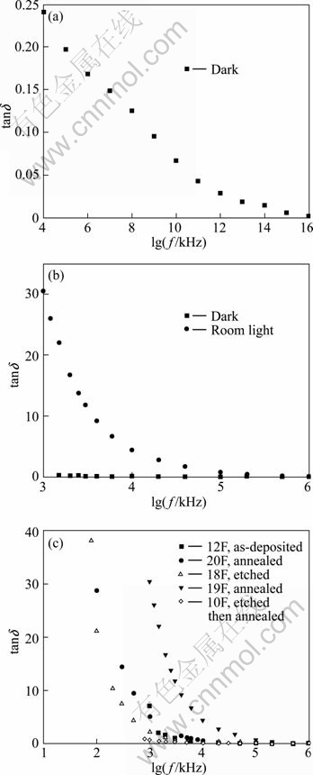
Fig. 6 Relation between dielectric loss tan�� and logarithm of frequency for CdS:In thin films: (a) For film in dark; (b) For film in dark and room light; (c) For as-deposited and treated films in room light
4 Conclusions
1) AC measurements were performed at room temperature in the dark and room light for as-deposited and treated CdS:In thin films prepared by the spray pyrolysis technique in the frequency range from 20 Hz to 1 MHz.
2) The real and imaginary parts of the impedance besides the total impedance and loss angle were investigated in the dark and room light as functions of frequency.
3) The response to light is found to have a decrease in these variables especially in the low frequency region.
4) It is found that the impedance has 1/f dependence on frequency in the high frequency range.
5) The relaxation time is estimated from the frequencies at which the imaginary part of the impedance is the maximum, where one relaxation time is estimated for each case.
6) The dielectric loss is found to decrease with frequency in accordance with the results obtained by other authors.
References
[1] Raza Khan Z, Zulfequar M, Shahid Khan M. Chemical synthesis of CdS nanoparticles and their optical, and dielectric studies [J]. J Mater Sci, 2011, 46: 5412-5416.
[2] Tsai C T, Chuu D S, Chen G L, Yang S L. Studies of grain size effects in rf sputtered CdS thin films [J]. J Appl Phys, 1996, 79(12): 9105-9109.
[3] MET?N H?LYA, ESEN R. Photoconductivity studies on CdS films grown by chemical bath deposition technique [J]. Erciyes ?niversitesi Fen Bilimleri Enstit��s�� Dergisi, 2003, 19(1/2): 96-102. (in Turkey)
[4] Perna G, Capozzi V, Ambrico M, Augelli V, Ligonzo T, Minafra A, Schiavulli L, Pallara M. Structural and optical characterization of undoped CdS films grown by pulsed laser deposition [J]. Thin Solid Films, 2004, 453/454: 187-194.
[5] Ikhmayies SHADIA J. Production and characterization of CdS/CdTe thin film photovoltaic solar cells of potential industrial use [D]. Amman: University of Jordan, 2002.
[6] IKHMAYIES SHADIA J, AHMAD-BITAR RIYAD N. The influence of the substrate temperature on the photovoltaic properties of spray-deposited CdS:In thin films [J]. Applied Surface Science, 2010, 256: 3541-3545.
[7] IKHMAYIES SHADIA J, AHMAD-BITAR RIYAD N. Effects of processing on the electrical and structural properties of spray-deposited CdS:In thin films [J]. Physica B: Condensed Matter, 2009, 404 (16): 2419-2424.
[8] IKHMAYIES SHADIA J, AHMAD-BITAR RIYAD N. Effects of annealing in nitrogen atmosphere and HCl-etching on the photoluminescence spectra of spray-deposited CdS:In thin films [J]. Applied Surface Science, 2009, 255(20): 8470-8474.
[9] IKHMAYIES SHADIA J, AHMAD-BITAR RIYAD N. Effect of film thickness on the electrical and structural properties of CdS: In thin films [J]. American Journal of Applied Sciences, 2008, 5(9): 1141-1143.
[10] IKHMAYIES SHADIA J, AHMAD-BITAR RIYAD N. Direct observation of infrared photoluminescence of spray-deposited CdS:In thin films [J]. J Luminouscence, 2008, 128(4): 615-619.
[11] Raji P, Sanjeeviraja C, Ramachandran K. Thermal and structural properties of spray pyrolysed CdS thin films [J]. Bull Mater Sci, 2005, 28(3): 233-238.
[12] AGASHE CHITRA, MARATHE B R, TAKWALE M G, BHIDE V G. Structural properties of SnO2:F films deposited by spray pyrolysis technique [J]. Thin Solid Films, 1988, 164: 261-264.
[13] El-Barry A M A, Atyia H E. Dielectric relaxation and AC conductivity of XS (X=Cd, Zn) compounds [J]. Physica B: Condensed Matter, 2005, 368: 1-7.
[14] Rinc��n M E, Mart��nez M W, Miranda-Hern��ndez M. Nanostructured vs polycrystalline CdS/ZnS thin films for photocatalytic applications [J]. Thin Solid Films, 2003, 425: 127-134.
[15] Ortu?o-L��pez M B, Valenzuela-J��uregui J J, Ram��rez-Bon R., Prokhorov E, Gonz��lez- Hern��ndez J. Impedance spectroscopy studies on chemically deposited CdS and PbS polycrystalline films [J]. Journal of Physics and Chemistry of Solids, 2002, 63: 665-668.
[16] IKHMAYIES SHADIA J, AHMAD-BITAR RIYAD N. The use of I-V characteristics for the investigation of selected contacts for spray-deposited CdS:In thin films [J]. Vacuum, 2011, 86: 324-329.
(Edited by YANG Bing)
Received date: 2011-07-26; Accepted date: 2011-11-14
Corresponding author: S. J. Ikhmayies; Tel: +962-79-5893884; E-mail: shadia_ikhmayies@yahoo.com

