Trans. Nonferrous Met. Soc. China 22(2012) s683-s687
Laser-assisted deposition of Cu bumps for microelectronic packaging
Won-Seok CHOI1, Joohan KIM 2
1. Department of Nano IT Fusion Program, Seoul National University of Science and Technology, Soeul 139-743, Korea;
2. Department of Mechanical and Automotive Engineering, Seoul National University of Science and Technology, Soeul 139-743, Korea
Received 21 May 2012; accepted 4 October 2012
Abstract: Cu bump was transferred using a focused laser pulse for microelectronic packaging. An Nd:YAG laser pulse (maximum energy of 500 mJ; wavelength of 1064 nm; fluences of 0.4-2.1 kJ/cm2) was irradiated on a sacrificial absorption layer with copper coating. The focused laser beam induced plasma between the semi-transparent donor slide and the sacrificial layer, causing a shock wave. The shock wave pressure pushed the Cu layer and transferred material to deposit a bump on substrate. A beam-shaper was used to produce uniform pressure at the interface to reduce fragmentation of the transferred material on the substrate. The calculated shock wave pressure with respect to laser fluence was 1-3 GPa. A Cu bump of diameter of 200 μm was successfully deposited at laser fluence of 0.6 kJ/cm2. The pressure control at the sacrificial layer using a laser pulse was critical to produce a bump with less fragmentation. The technique can be applied to forming Cu bump for an interconnecting process in electronics.
Key words: laser induced forward transfer; bump deposition; Nd:YAG pulsed laser; micro system packaging; beam shaping
1 Introduction
The laser technology has been developed in various micro fabrication applications due to its unique characteristics of high precision and non-contact energy control. Material deposition, transfer, and removal are important in the microsystem packaging process and laser micro cutting, laser micro soldering and bonding can be applied for these applications. As reduction of mass and thickness of electronics becomes more important, the interconnection technology for electronic components and printed circuit boards (PCB) become crucial. Conducting bumps have been used to connect these electrical components and the size of bumps has also been reduced because the smaller bumps provide short responds and reduced delay times. The conventional bump fabrication can be classified into solder jet [1], evaporation [2], screen printing [3], electroplating [3], and ball placement [4,5]. Each process has its own advantages. There are, however, several disadvantages in these processes such as a long process time, a large bump size, environmental hazards and ball locating difficulties, respectively.
A selective material transfer from a thin film using laser has been developed since 1980s [6]. Matrix-assisted pulsed laser evaporation (MAPLE) was reported to deposit molecular size materials [7]. Moreover, laser-induced forward transfer (LIFT) [8,9] using donor film has been developed to deposit designed materials with high precision[8]. When a metal layer on a semi-transparent slide (donor) is exposed to a focused laser beam, a shock wave can be generated and by using this energy, the material can be transferred and deposited on the substrate. This process enables the ability to deposit various materials on different substrates [10]. This selective material transfer can be applied to deposition of metal bumps on substrate without any mask or pre-processes.
In this study, an attempt was made to deposit a Cu bump on a substrate using a modified laser beam. The spatial laser beam intensity distribution of a regular laser beam is Gaussian, which has a peak at the center. When this kind of beam is applied to transferring materials in LIFT, the power density at the center of a laser spot can be over the ablation fluence, inducing a hot spot at the center of the laser beam. It generally leads to large deposition fragmentation. A beam shaper was adopted to produce a flat-top beam shape from a Gaussian energy distribution and its effect was investigated. Various deposited bumps were obtained and analyzed.
2 Experimental
The laser process scheme is shown in Fig. 1. The donor was prepared by applying a sacrificial absorption layer (Polyethylene) and a metal layer (Cu) on a thin glass slide. The thickness of the sacrificial absorption layer and the metal layer are 6 μm and 100 μm, respectively. The material property of Cu is given in Table 1. It was expected that a sacrificial absorption layer could reduce any the thermal effects to the metal layer[9]. A modified laser beam by a beam shaper was used to induce a uniform pressure wave in transferring Cu onto the substrate. The distance between the donor and the target substrate was around 150 μm. After Cu was transferred, a fresh region of the donor film was supplied by moving it with linear-motorized stages.
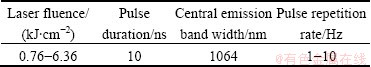
The experimental setup is shown in Fig. 2. A flash-lamp type Nd:YAG laser (pulse: maximum energy of 500 mJ; wavelength of 1064 nm) was used and beam delivery optical systems which includes infrared mirrors, beam splitters and an objective lens. A pulse laser beam with fluences of 0.4-2.1 kJ/cm2 was applied. The laser spot and its beam shape could be identified by using photosensitive papers. Linear-motorized stages were used to move the thin glass slide to supply a fresh part of a coating layer. The experimental parameters used in this study are summarized in Table 2. The transferred bump was examined with an optical microscope (Olympus micro-scope 10X, BX51M).
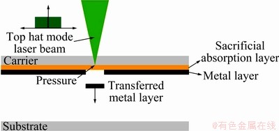
Fig. 1 Schematic diagram of laser-assisted bump deposition process
Table 1 Properties of transferred metal layer (Cu)
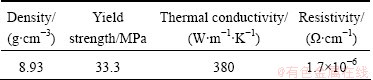
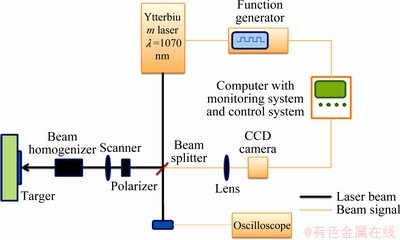
Fig. 2 Experimental setup
Table 2 Experimental condition
The generated pressure from laser ablation of the sacrificial layer is proportional to laser pulse intensity. However, the Gaussian laser beam has its maximum energy density at the center. This energy distribution may lead to a hot spot at the center and the shock wave generation would be not uniform, which is not good for transferring materials. The principal challenge in using a laser pulse was in determining how to achieve a uniform energy distribution at the interface. A laser beam shaper (Focal pi-Shaper; MOLTECH 1064c) was applied to reshaping the beam profile. The Gaussian laser energy distribution of the beam could be changed into a flat-top shape or various types by applying an offset from the focal plane. The various profiles of a laser beam used in this experiment are shown in Fig. 3.
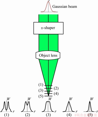
Fig. 3 Beam shapes with respect to offsets from focal plane
3 Laser-induced shock wave pressure
The sacrificial layer of the donor film absorbs the laser energy and plasma with a shock wave is generated at the interface of a glass slide and the sacrificial layer. At that time, the pressure magnitude is important and should be calculated to understand the transfer mechanism. FABBRO et al [11] reported the relation between laser intensity and the magnitude of pressure. When the constant laser intensity with respect to time is assumed, the developed formula is as follows:
 (1)
(1)
where α is the fraction of the internal energy devoted to the thermal energy; Z is the impedance which covers plasma and Ip is the absorbed laser intensity. The value of α is 0.1 g/(cm2・s) in the case of 1064 nm of the wavelength of the laser beam and 10 ns of the laser pulse width. Because the shock wave is generated between a thin glass slide and a polymer layer, the impedance must be evaluated with two sub-impedances with the following equation:
 (2)
(2)
where Z1 is an impedance for the thin glass slide and Z2 is an impedance of the sacrificial polymer layer. The relation between the shock wave pressures with respect to pulse energy was calculated and shown in Fig. 4. When a laser pulse was irradiated on the target, the calculated pressure from the shock wave at the interface was around 1 GPa. It can be considered that this value is large enough to push the metal layer from the glass slide and transfer the material to the substrate.
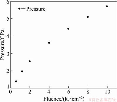
Fig. 4 Laser fluence vs shock wave pressure
4 Results and discussion
The shape of spatial beam affected the material transfer. Therefore, different spatial beam shapes were applied in order to explore its effect. The results of material deposition with respect to various beam profiles are shown in Fig. 5 and Fig. 6. Thin polymer coating instead of Cu layer was used to clearly identify the deposition shape with respect to beam profiles. The result of original laser transfer without beam shaping is shown in Fig. 5. A hole is observed in Fig. 5(a) as a result of the material transfer from the sacrificial layer. The size of the transferred material is larger than its original one on the sacrificial layer as shown in Fig. 5(b). This can be explained as follows. The Gaussian beam profile providing the highest beam energy at the center causes a pressure difference at the interface of the transferred materials and the sacrificial layer. It is also thought that a micro explosion of a sacrificial layer by a concentrated energy distribution might have occurred instead of just cutting and pushing the transferring material. The spatial beam shape can be changed by a beam shaper which is described previously. Various beam profiles are obtained by applying offsets from a focal plane as shown in Fig. 6. At the focal plane, the material is mainly deposited around the center (offset of 0 mm; a Gaussian shape beam). When the flat-top shape beam is used, a well aggregated deposition can be observed (offset of 0.5 mm; a flat-top shape beam). A large fragmentation diameter is also measured with an M-shape beam (offset of 1.0 mm; an M-shape beam). This result shows that a properly shaped beam can be used for a well-defined material transfer. The homogenous laser energy distribution is not directly related to the homogenous pressure distribution. Meanwhile, it is thought that a threshold fluence of a laser beam of the sacrificial layer is closely related to the pressure distribution. However, the experimental results indicate that the homogenous energy distribution of a laser beam can produce less fragmented deposition. It is concluded that an improved material transfer can be obtained with proper laser beam shaping.
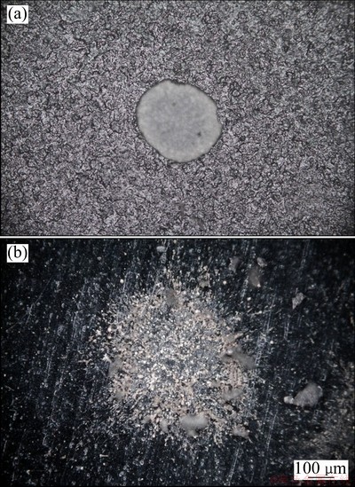
Fig. 5 Beam profiles of sacrificial layer (a) and transferred material (b)
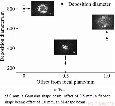
Fig. 6 Offsets from focal plane vs deposition diameter
A flat-top profile laser beam was used to produce a uniform pressure on the Cu coating layer. The results of Cu deposition with various laser fluences are shown in Figs. 7 and 8. As the laser fluences increases, the level of fragmentation increases. The Cu layer is pushed out by the pressure at the sacrificial absorption layer and melting of the transferred material can be observed. The melting or ablation will be significant if there is no sacrificial absorption layer. The increasing rate of the fragmentation diameter is high at low laser pulse fluence and it means that the aggregation of deposited material is sensitive in that region. The minimum diameter of Cu bump is around 200 μm and it is thought that even a smaller Cu bump can be transferred with a precision energy control and beam shaping.
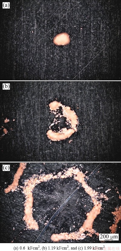
Fig. 7 Cu bump deposition with various laser fluences
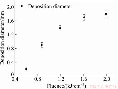
Fig. 8 Laser fluence vs deposition diameter
5 Conclusions
An investigation of laser induced forward transfer for deposition of Cu pumps using beam shaping for microsystem packaging has been described. When a laser beam was irradiated on the sacrificial absorption layer of a glass slide, a pressure by a shock wave pushed the Cu metal layer out locally and material transfer and deposition could be achieved. The calculated pressure with respect to laser fluence was 1-3 GPa. A Cu bump with diameter of 200 μm was deposited successfully at a laser fluence of 0.6 kJ/cm2. A large fragmentation was observed in the case of using non-uniform beam such as a Gaussian beam. Beam shaping was adopted to solve this problem and it could be used to produce a uniform pressure distribution at the interface between the sacrificial layer and the coating layer. In addition, a precision control of laser fluence was a crucial factor to obtain a well-defined Cu bump deposition, too.
References
[1] DIAO H, WANG C, ZHAO Z, TIAN Y, KONG L. Interfacial reactions between Sn-Cu solder alloy and Cu/Ni coatings during reflow soldering [J]. The Chinese Journal of Nonferrous Metals, 2007, 17(3): 410-416.
[2] ESROM H, ZHANG J, KOGELSCHATZ U, PEDRAZA A J. New approach of a laser-induced forward transfer for deposition of patterned thin metal films [J]. Applied Surface Science, 1995, 86: 202-207.
[3] NOH J H, LEE T M, JO J D, LEE S H, KIM D S. A study of design and manufacture of metal jet system for ultra fine solder ball [J]. The Korean Society of Mechanical Engineers, 2010: 339-340.
[4] KIM K S, KIM J Y. A study on the ball-off of via balls bonded by solder paste [J]. Journal of the Korean Institute of Electrical and Electronic Material Engineers, 2004, 17(6): 575-579.
[5] ABTEW M, SELVADURAY G. Lead-free solders in microelectronics [J]. Materials Science and Engineering A, 2000, 27: 95-141.
[6] DHAMI G, TAN B, VENKETAKRISHNAN K. Laser induced reverse transfer of gold thin film using FEM to second laser [J]. Optics and Lasers in Engineering, 2011, 49: 866-869.
[7] SMAUSZ T, HOPP B, KECSKEMETI G, BOR Z. Study on metal microparticle content of the material transferred with absorbing film assisted laser induced forward transfer when using silver absorbing layer [J]. Applied Surface Science, 2006, 252: 4738-4742.
[8] FARDEL R, NAGEL M, NUESCH F, LIPPERT T, WOKAUN A. Laser forward transfer using a sacrificial layer: Influence of the material properties [J]. Applied Surface Science, 2007, 254: 1322-1326.
[9] FARDEL R, NAGEL M, NUESCH F, LIPPERT T, WOKAUN A. Shadowgraphy investigation of laser-induced forward transfer: Front side and back side ablation of the triazene polymer sacrificial layer [J]. Applied Surface Science, 2009, 255: 5430-5434.
[10] PAPADOPOULOU E L, AXENTE E, MAGOULAKIS E, FOTAKIS C, LOUKAKOS P A. Laser induced forward transfer of metal oxides using femtosecond double pulses [J]. Applied Surface Science, 2010, 257: 508-511.
[11] FABBRO R, FOURNIER J, BALLARD P, DEVAUX D, VIRMONT J. Physical study of laser produced plasma in confined geometry [J]. Applied Surface Science, 1990, 68(2): 775-784.
(Edited by ZHAO Jun)
Foundation item: Project (2012-0001900) supported by the National Research Foundation of Korea
Corresponding author: Joohan KIM; Tel: +82-10-48529674; E-mail: joohankim@seoultech.ac.kr
DOI: 10.1016/S1003-6326(12)61786-5

