Modeling transmittance through submicron silver slit arrays
来源期刊:中南大学学报(英文版)2012年第8期
论文作者:王爱华 蔡九菊 陈玉彬
文章页码:2107 - 2114
Key words:finite difference time domain method; transmittance; silver slit array; cavity resonance effect
Abstract: Mid-infrared transmittance of submicron silver slit arrays was numerically studied with the finite difference time domain method. The slit width varies from 50 nm to 300 nm and a square feature may attach at either or both slit sides. Although the side length of features is one or two orders of magnitude shorter than the wavelength, the attached nanoscale features can modify the transmittance significantly. The transmittance was also further investigated in detail by looking into the electromagnetic fields and Poynting vectors of selected slit geometries. The investigation results show that such change can be attributed to the cavity resonance effect inside the slit arrays. The work is of great importance to the wavelength-selective devices design in optical devices and thermal application fields.
J. Cent. South Univ. (2012) 19: 2107-2114
DOI: 10.1007/s11771-012-1252-6![]()
WANG Ai-hua(王爱华)1, CAI Jiu-ju(蔡九菊)1, CHEN Yu-bin(陈玉彬)2
1. School of Materials and Metallurgy, Northeastern University, Shenyang 110819, China;
2. Department of Mechanical Engineering, Center for Micro/Nano Science and Technology,
National Cheng Kung University, Tainan City, 701, China
? Central South University Press and Springer-Verlag Berlin Heidelberg 2012
Abstract: Mid-infrared transmittance of submicron silver slit arrays was numerically studied with the finite difference time domain method. The slit width varies from 50 nm to 300 nm and a square feature may attach at either or both slit sides. Although the side length of features is one or two orders of magnitude shorter than the wavelength, the attached nanoscale features can modify the transmittance significantly. The transmittance was also further investigated in detail by looking into the electromagnetic fields and Poynting vectors of selected slit geometries. The investigation results show that such change can be attributed to the cavity resonance effect inside the slit arrays. The work is of great importance to the wavelength-selective devices design in optical devices and thermal application fields.
Key words: finite difference time domain method; transmittance; silver slit array; cavity resonance effect
1 Introduction
Sub-wavelength periodic structures have demonstrated wavelength- or polarization-selective radiative properties, which are critical for many optical devices and thermal applications [1]. For example, one-dimensional metallic slit arrays could boost the development of nanolithography and energy conversion devices such that their unique radiative properties were investigated both numerically and experimentally [2]. Their enhanced transmittance was attributed to several physical mechanisms, including Wood’s anomaly, cavity resonance, and effective medium behavior [3]. Obviously, either one or the interplay of multiple mechanisms can tailor the spectrum of radiative properties with strong dependence on slit geometry. Though correlations between tailoring mechanisms and unique radiative properties have attracted abundant research interests, various slit geometries with exactly rectangular cross-section are assumed for metallic strips in most numerical investigations. The geometry variation could be slit width, slit depth or period [4-6]. Other types of slit array are composed of alternative rectangular metallic and dielectric strips or each rectangular strip is partially filled with dielectrics [7-8]. Some researches have been conducted recently in understanding the transmission behavior in sub-wavelength metallic slits. DI studied the effects of different metal materials and slit shapes on the transmission behavior for the horn-opened sub-wavelength metallic slits with the incident wavelength from 500 nm to 750 nm [9]. LI simulated the transmittance of the funnel-shaped slit structures and found that the transmittance peak position is dependent on the structural parameters [10]. KONG et al investigated the interaction of cavity structures, such as a single slit, a single groove or slit-groove-grating structure, embedded in metal films with illuminating light by employing the finite difference domain time method [11]. LEE et al [12] investigated the transmission enhancement through nanoscale metallic slit arrays in the wavelength range from visible to mid-infrared.
However, the expectation of smooth side walls and sharp corners for periodic structures is not always met during micro/nanofabrication [13]. Either photoresist residues or the intrinsic limits of fabrication process may cause imperfection of structure features, leading to radiative property discrepancy from numerical modeling. Though the discrepancy may come from measurement uncertainty and other reasons, little research has been done on effects of slit feature variation, specifically the slit profile. In fact, effects of tiny variation are not necessarily negligible at long wavelengths although this assumption is well-accepted. Another questionable assumption is the large transmittance through wide slit opening at any wavelength. On the other hand, it is hoped that radiative properties can be strongly modified by intentionally-fabricated irregular features. In that case, slit arrays with non-rectangular cross-section may offer an additional freedom for practitioners to manipulate radiative properties.
Hence, the objective of this work is to study the effects of tiny cross-section variation on transmittance of nanoscale slit arrays at long wavelengths ranging from 3 μm to 15 μm. Infrared (IR) is the main part of thermal radiation but IR radiative properties of metallic slits are rarely discussed. Only a few structure variations will be looked into for simplicity because this work is an initiation and feature variation can be many types. Furthermore, the potential mechanisms tailoring radiative properties of irregular slit arrays based on electromagnetic (EM) fields and time-averaged poynting vectors (S) are also studied. Silver is selected as the material of metallic strips as well as attached features owing to its ideal physical and optical properties. The malleability and ductility of silver minimize the difficulty in nanoscale fabrication, especially for non-rectangular metallic strips. Additionally, the resistance of silver to oxidization maintains structure geometry and high reflectivity at the IR incidence.
2 Model development and numerical methods
2.1 Geometry and optical constants
Since modeling results should be applicable to structures above a supporting transparent substrate in practice, different free-standing structures are considered in this work for simplicity. The structures include a thin film as the reference case, slit arrays with varied slit width (w), and arrays of non-rectangular metallic strip. For the non-rectangular metal strip, a square feature may attach at either both slit sides and locate at the inlet facing the transverse magnetic (TM) wave incidence. The cross-section schematic of attached features is a square with each side length of a, as shown in Fig. 1. The thickness (d) is fixed at 110 nm for all structures and the period (Λ) of slits is set to be 800 nm, which is the summation of strip width (l) and slit width (w). That is, the metallic filling ratio (f ) is defined as f = l/Λ. On the other hand, the slit width changes from 50 to 300 nm and the side length (a) of all features is less than 50 nm. This work focuses on two types of feature attachment at slit inlet: single convex square and double convexes squares. Therefore, the smallest feature side and the narrowest slit opening are 10 nm and 20 nm, respectively. A representative slit array is selected among possible combinations for convenience and its dimensions are d=110 nm, w=50 nm, and Λ=800 nm.
Figure 1 shows the freestanding slits in vacuum with square features attaching both walls symmetrically at the slit inlet. The TM wave is incident from vacuum in Region I. Region II is composed of medium silver and free space such that the dielectric function is a periodic function of x with the period Λ. Here, Region II is divided into two slabs with different thicknesses because f is different in each slab. In Fig. 1, the wavevector k defines the direction of incidence, and the angle between k and the surface normal z is the angle of incidence θ. For the TM wave, the magnetic field H is perpendicular to the plane of incidence (the x-z plane), i.e., parallel to the y-direction.
In contrast to complicated geometry variation, only two media, silver and free space, are considered. The slit is free space with the dielectric function ε=(n+iκ)2=1, which is the same as that of regions above and below slit arrays. Optical constants n and κ are the refractive index and extinction coefficient, respectively. On the other hand, the dielectric function ε of Ag is obtained from the Drude model and can be expressed as [1]
![]() (1)
(1)
where ω=2πc/λ, is the angular frequency, with c and λ being the speed of light and wavelength in vacuum, respectively; ?∞ is the high-frequency limiting value; ωp is the plasma frequency and λc is the scattering rate. The scattering rate and plasma frequency of Ag are taken from Refs. [14-15].
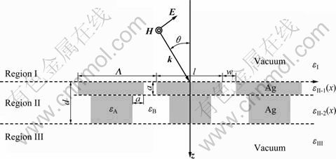
Fig. 1 Illustrations of device and model structures (TM mode)
2.2 Finite difference time domain method
The numerical algorithm employed here includes thin-film optics formulation [16] and the finite difference time domain (FDTD) method [17]. The thin-film optics formulation is only for efficient modeling of freestanding film.
The FDTD method can directly model the electromagnetic wave propagation via numerically solving the Maxwell’s equations and is a central difference scheme in both time and space domains with the second-order accuracy. Maxwell’s equations take the following form for a linear isotropic material:
![]() (2)
(2)
![]() (3)
(3)
where E and H represent the electric and magnetic fields, respectively; Js and Ms are the electrical and magnetic field sources, respectively; ![]()
![]()
![]() and
and ![]() are the permittivity, permeability, electrical conductivity, and magnetic conductivity or equivalent magnetic loss of the material, respectively. Note that
are the permittivity, permeability, electrical conductivity, and magnetic conductivity or equivalent magnetic loss of the material, respectively. Note that ![]() where ε0 is the permittivity value in vacuum. In the current problem, Js and Ms are zero. In this work, the 1D slit structures have to be solved in the 2D space. Maxwell’s equations are split into two sets for two polarizations: the transverse electric (TE) polarization and the TM polarization. Furthermore, since the material properties are complex numbers, to adapt them to real number computation, their equivalent real properties εe and σe are used.
where ε0 is the permittivity value in vacuum. In the current problem, Js and Ms are zero. In this work, the 1D slit structures have to be solved in the 2D space. Maxwell’s equations are split into two sets for two polarizations: the transverse electric (TE) polarization and the TM polarization. Furthermore, since the material properties are complex numbers, to adapt them to real number computation, their equivalent real properties εe and σe are used.
The detailed numerical scheme, periodic boundary treatment, and perfectly matched layer absorbing boundary condition can be found in Ref. [17], so they are not repeated here. Only the essential difference equations are presented below. For a 2D geometry, by replacing the electric and magnetic fields with their vector components and employing the equivalent properties, the solutions for the TM wave with a second-order central-difference scheme can be written as
![]()
![]()
![]() (4a)
(4a)
![]()
![]() (4b)
(4b)
![]()
![]() (4c)
(4c)
where the superscript of the field components stands for time step index (n) and the subscript represents the vector component: x is the grating groove direction, z is the height direction and y is normal to the paper plane. Δt is the time step size used in the time derivative terms. Note that in Eq. (4), σe and σM are set to be zero for dielectric and non-magnetic materials. According to YEE’s notation [17], a spatial point in a Cartesian coordinate that is written as (i, j) corresponds to the coordinate (iΔx, jΔz), where Δx and Δz are the lattice space increments in the x and z directions, and i and j are integer indices.
2.3 Recursive convolution treatment of Drude model
The Maxwell-Ampere law with the complex forms of ![]() and
and ![]() for a time harmonic incident field in the Maxwell’s equations is as follows
for a time harmonic incident field in the Maxwell’s equations is as follows
![]()
![]()
![]() (5)
(5)
To distinguish from ε, the dielectric function or dielectric constant is expressed as ![]() σe and εe are equivalent properties and used in the FDTD equations. When n2-κ2=?′=εe/εo<0, the FDTD code cannot converge because the coefficient of the first term on the right hand side of FDTD equations and similar difference equations is greater than 1 and the second term is smaller than the first term. This means Ez or H field components could have non-steady or large oscillations through time stepping. Thus, the time stepping does not lead to a converged Ez field. Many metals in the wavelength of interest, such as infrared, have large negative ?'. Special treatment for such property in the difference equations is needed and discussed below.
σe and εe are equivalent properties and used in the FDTD equations. When n2-κ2=?′=εe/εo<0, the FDTD code cannot converge because the coefficient of the first term on the right hand side of FDTD equations and similar difference equations is greater than 1 and the second term is smaller than the first term. This means Ez or H field components could have non-steady or large oscillations through time stepping. Thus, the time stepping does not lead to a converged Ez field. Many metals in the wavelength of interest, such as infrared, have large negative ?'. Special treatment for such property in the difference equations is needed and discussed below.
Optical properties of the metal with free electron are usually described by the Drude model [1]. Using the convolution integral, the frequency domain relation of the displacement vector and electric vector can be converted into a time domain relation [18]. Assuming 1D case for simplicity, a new difference equation of the electric field vector component is derived:
![]()
![]()
![]() (6)
(6)
where c0 is a time domain susceptibility at the zero-th time step. It is further simplified to a recursive relation so the summation and the storage of the earlier time step electric field can be avoided. As can be seen in Eq. (6), the coefficient problem in the original FDTD equation is eliminated.
In this work, one-dimensional slits are solved in two-dimensional space and equivalent real property rather than a complex dielectric function is adapted. Numerical codes based on the algorithm were programmed by WANG et al and were successfully used for modeling radiative properties of nanoscale structures in Refs. [19-21]. The mesh size of FDTD calculations used was 5 nm. The time step size was in the order of 10-16 s following the Courant-Friedrichs-Lewy criterion [18].
3 Results and discussion
3.1 Transmittance of freestanding film and slits
Figure 2 shows the transmittance spectra of selected freestanding film and slit array as guidance in understanding the transmittance. The spectral region (3 μm≤λ≤15 μm) covers from near to mid-IR. The normal incidence is considered and the spectra are presented in the same logarithmic scale for comparison.
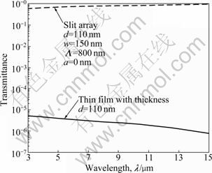
Fig. 2 TM wave transmittance through freestanding silver structures in vacuum at normal incidence
As can be seen from Fig. 2, since the thickness of the freestanding film is much more than the penetration depth, the transmittance is less than 1×10⁻⁵. Although the transmittance is almost one order of magnitude lower at long wavelengths, any explanation to the spectrum variation should be given with caution due to the low transmittance. For the transmittance of slit array with the same thickness as the film, the slit opening is 150 nm wide such that the metallic filling ratio is 0.812 5. However, the transmittance is larger than 0.6 and increases with the wavelength due to the well-known effective medium behavior [4]. Based on two curves in Fig. 2, it is clear that most TM wave incidence is reflected by the 110 nm thick silver film but transmitted through nanoscale slit arrays.
Figure 3 show the TM wave transmittance through 110 nm thick freestanding silver slit arrays with different geometry variations at normal incidence. Figure 3(a) demonstrates the TM wave transmittance through silver slit arrays with different slit widths at normal incidence. The transmittance is low at short wavelengths and increases monotonically with the wavelength. However, the transmittance is not proportional to the slit width and its value strongly depends on the wavelength. At λ=3 μm, the transmittance is about 0.10, 0.30, 0.6, and 0.8 for w= 50, 100, 200, and 300 nm, respectively. On the other hand, the transmittance is above 0.95 at λ=15 μm for w= 200 and 300 nm. As a result, one may expect that small variation in the slit width may affect the transmittance, but the variation effects become trivial for wide slits at long wavelengths.
Figure 3(b) compares the transmittance through 300 nm wide slits with various attached squares. The attached square features can be at one wall (single convex) or both walls (double convexes). For single convex attachment, square features at either side are the same due to the normal incidence. The side length of squares includes a=10, 30, or 50 nm. Four transmittance spectra shown in the figure represent single convex with a=10 or 30 nm and double convexes with a=30 or 50 nm attachment individually. Similar to the spectra in Fig. 3(a), the four spectra change little at short wavelengths and almost the same at long wavelengths. It is clear that double-convex squares with a=50 nm do not modify the transmittance much, even the opening width shrinks to 200 nm, which is 2/3 of the original width. Such transmittance spectrum is close to that of w= 200 nm (the same slit opening width) as shown in Fig. 3(a), especially at long wavelengths. The difference becomes noticeable when the wavelength gets short and the transmittance is not large.
The transmittance through 100 nm wide slit with/ without features is shown in Fig. 3(c). Since the width of slits significantly reduces, the transmittance for both single and double square attachment also decreases, especially at short wavelengths. The reduction in transmittance is approximately proportional to the size increment of the square attachment. However, the transmittance spectrum of double convexes shows abrupt change at about λ=5 μm, but the change is not shown in other spectra. The exact wavelength of abrupt changes is not the same for different square sizes. Due to these changes, the transmittances at short wavelengths are the same for 10 nm single convex and double convexes attachment. Note that the slit opening is only 40 nm wide for double attached a=30 nm convexes, but its transmittance in the whole spectrum is still larger than that through 50 nm wide slits as shown in Fig. 3(a). In this case, the narrow opening may not block transmittance as effectively as slits of the same narrow width.
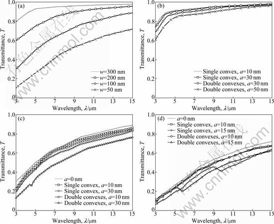
Fig. 3 TM wave transmittance through 110 nm thick freestanding silver slit arrays at normal incidence (d=110 nm, θ=0°, Λ=800 nm): (a) w=50, 100, 200, and 300 nm without any attached features; (b) w=300 with a=10, 30, and 50 nm square features; (c) w=100 nm with a=10 and a=30 nm square features; (d) w=50 nm with a=10 and a=15 nm square features
Transmittance through 50 nm wide slits with the square feature size of a=10 or 15 nm is shown in Fig. 3(d). One interesting effect of such narrow slits is that the attached features reduce transmittance more at long wavelengths than at short ones. When the length size of square enlarges from a=10 to a=15 nm, the transmittance modifies a little for single convex attachment. On the other hand, the abrupt changes in spectra for double convexes become significant. Specifically, the transmittance through slits with a= 15 nm square attachment is sometimes larger (λ≈10.5 μm) or very close (λ≈5.7 μm) to that with a=10 nm squares. Or, in another way, there are unusual dips of a=10 nm curve at the aforementioned wavelengths.
3.2 Electromagnetic fields and Poynting vectors
Figure 4 shows the square of the magnitude of magnetic field (i.e., lg|Hy|2) and the normalized time-averaged Poynting vector (i.e., lg|S|/|Sinc|) for three types of slit in the logarithmic scale. The subscripts y and “inc” are for the y-component and incidence, respectively. That is, the Poynting vector is normalized to that of incidence, whose wavelength is 10.0 μm for investigation. In Fig. 4, the incidence propagates along the z-axis direction. Dimensions of all slits are the same as those of representative slits, except that attached features are different. Three types of feature variations include no square attachment for Figs. 4(a) and 4(b), double a= 10 nm convexes for Figs. 4(c) and 4 (d), and double a= 15 nm convexes for Figs. 4(e) and 4(f). The magnitude of magnetic field is shown in Figs. 4(a), 4(c), and 4(e), while the magnitude of normalized time-averaged Poynting vector is plotted in other three figures. Obviously, only Figs. 4(c) and 4(d) show unique patterns like standing waves within slits. The attached features do not act as those in Figs. 4(e) and 4(f) to block the incidence. On the contrast, magnitudes of the magnetic field and Poynting vector are higher than those shown in Figs. 4(a) and 4(b). In this case, the incidence may penetrate the features freely and excite resonance inside the cavity.
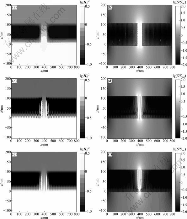
Fig. 4 Complex magnetic field ((a), (c) and (e)) and normalized Poynting vector ((b), (d) and (f)) for representative silver slit arrays with TM wave at normal incidence and wavelength λ=10 nm: (a) No attached square (a=0 nm); (b) No attached square (a=0 nm); (c) Double a=10 nm square features attached; (d) Double a=10 nm square features attached; (e) Double a=15 nm square features attached; (f) Double a=15 nm square features attached
Further steps are taken to see how the transmittance is funneled through slits and where the energy is absorbed. In Fig. 5, the time-averaged Poynting vectors around slit region are plotted for slits at normal incidence discussed previously. Metallic strips and features are also marked with semi-transparent shadows for reading convenience. The arrows tell directions of the Poynting vector and indicate the path of net energy flow. The magnitude of Poynting vector inside slits is greater than that of Regions I and III and is marked with longer arrows. In Fig. 5(a), the energy is squeezed into the narrow slits with negligible transmittance through metallic strips. Poynting vectors inside the slit are aligned well with the same magnitude, except those located around strip corners. Those vectors show that the largest magnitude among all vectors may result from the abrupt change of material properties. In Fig. 5(b), the Poynting vectors inside slits are not well-aligned and the magnitude is not same all the way through slits. Some Poynting vectors may even penetrate the attached features, leading to the induced absorptance. After partial energy is absorbed due to the attached features, the transmittance through slits is therefore reduced such that the transmittance through slits in Fig. 5(b) is the smallest. However, when the feature size is further enlarged, as shown in Fig. 5(c), the Poynting vector cannot penetrate features but squeeze into the narrow opening. Therefore, the transmittance is lower than that in Fig. 5(a).
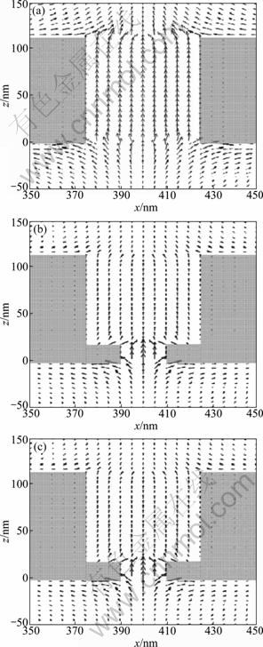
Fig. 5 Contour plots of Poynting vector distributions at TM wave normal incidence for representative silver slit arrays: (a) No attached square features; (b) Double a=10 nm square features attached; (c) Double a=15 nm square features attached
4 Conclusions
1) For the slit structures without square features attachment, the transmittance increases monotonically with the wavelength, but is not proportional to the slit width.
2) Given the slit structures with square features at the inlet, the effects of square features attachment mode and side length on the transmittance are different for the various slit widths.
3) Based on the analysis of electromagnetic field and Poynting vectors, such transmittance change can be attributed to the cavity resonance effect inside the slit arrays.
References
[1] ZHANG Z M. Nano/microscale heat transfer [M]. New York: McGraw-Hill, 2007: 32-47.
[2] CHEN Y B, LEE B J, ZHANG Z M. Infrared radiative properties of submicron metallic slits [J]. Journal of Heat Transfer, 2008, 130(8): 082404-082411.
[3] CROUSE D, KESHAVAREDDY P. Polarization independent enhanced optical transmission in one-dimensional gratings and device applications [J]. Optical Express, 2007, 15(4): 1415-1427.
[4] LEE B J, CHEN Y B, ZHANG Z M. Confinement of infrared radiation to nanometer scales through metallic slit arrays [J]. Journal of Quantitative Spectroscopy and Radiative Transfer, 2008, 109(4): 608-619.
[5] PENDRY J B. Radiative exchange of heat between nanostructures [J]. Journal of Physics: Condensed Matter, 1999, 11(35): 6621-6628.
[6] MOREAU A, LAFARGE C, LAURENT N, EDEE K, GRANET G. Enhanced transmission of slit arrays in an extremely thin metallic film [J]. Journal of Optics A: Pure and Applied Optics, 2007, 9: 165-169.
[7] CROUSE D, KESHAVAREDDY P. Role of optical and surface plasmon modes in enhanced transmission and applications [J]. Optics Express, 2005, 13(20): 7760-7771.
[8] MIN C J, JIAO X J, WANG P, MIN H. Investigation of enhanced and suppressed optical transmission through a cupped surface metallic grating structure [J]. Optics Express, 2006, 14(12): 5657-5663.
[9] DI Si. The study of extraordinary transmission behavior in sub-wavelength metallic slit [D]. Beijing: Beijing Jiaotong University, 2006. (in Chinese)
[10] LI Zhu-bin. Optical transmission behavior in periodically sub-wavelength structures [D]. Tianjin: Nankai University, 2008. (in Chinese)
[11] KONG Xian-tian, LI Zhu-bin, TIAN Jian-guo. Interaction of light and cavity structures in metal film [J]. China Science Paper Online, 2010, 7: 1-7. (in Chinese)
[12] LEE B J, CHEN Y B, ZHANG Z M. Transmission enhancement through nanoscale metallic slit arrays from the visible to mid-infrared [J]. Journal of Computational and Theoretical Nanoscience, 2008, 5(2): 201-213.
[13] BARBARA A, QUEMERAIS P, BUSTARRET E, LOPEZ-RIOS T. Optical transmission through subwavelength metallic gratings [J]. Physics Review B, 2002, 66(16): 161403-161412.
[14] ORDAL M A, LONG L L, BELL R J, Alexander R W, WARD C A. Optical properties of the metals Al, Co, Cu, Au, Fe, Pb, Ni, Pd, Pt, Ag, Ti, and W in the infrared and far infrared [J]. Applied Optics, 1983, 22(7): 1099-1119.
[15] PALIK E D. Handbook of optical constants of solids [M]. San Diego: Academic Press, 1998: 436-441.
[16] YEH P. Optical waves in layered media [M]. New York: Wiley, 1988: 154-162.
[17] TAFLOV A, HAGNESS S C. Computational electrodynamics: The finite-difference time-domain method [M]. 3rd ed. Boston: Artech House, 2005: 75-110.
[18] KUNZ K S, LUBBERS R J. The finite difference time domain method for electromagnetics [M]. Boca Raton: CRC Press, 1993: 214-220.
[19] WANG A H, CAI J J. Modeling radiative properties of nanoscale patterned wafers [J]. China Science: Technological Sciences, 2010, 53(2): 352-359.
[20] WANG A H, CAI J J. Pattern scaling effect on the radiative properties of Wafer’s surface [J]. China Science: Technological Sciences, 2010, 53(7): 1886-1892.
[21] WANG A H, HSU P F, CHEN Y B, CAI J J. Effect of nanoscale features on infrared radiative properties of heavily doped silicon complex gratings [J]. China Science: Technological Sciences, 2010, 53(8): 2207-2214.
(Edited by HE Yun-bin)
Foundation item: Project(N110402015) supported by the Fundamental Research Funds for the Central Universities of China; Project(2012M510075) supported by China Postdoctoral Science Foundation
Received date: 2011-07-01; Accepted date: 2012-02-20
Corresponding author: WANG Ai-hua, PhD; Tel: +86-13624210542; E-mail: wangaihua1976@yahoo.com.cn

