
J. Cent. South Univ. (2018) 25: 1678-1689
DOI: https://doi.org/10.1007/s11771-018-3859-8

Experimental investigation of subsurface damage depth of lapped optics by fluorescent method
WANG Hong-xiang(������), HOU Jing(�), WANG Jing-he(������),ZHU Ben-wen(�챾��), ZHANG Yan-hu(���廢)
School of Mechatronics Engineering, Harbin Institute of Technology, Harbin 150001, China
 Central South University Press and Springer-Verlag GmbH Germany, part of Springer Nature 2018
Abstract: Subsurface defects were fluorescently tagged with nanoscale quantum dots and scanned layer by layer using confocal fluorescence microscopy to obtain images at various depths. Subsurface damage depths of fused silica optics were characterized quantitatively by changes in the fluorescence intensity of feature points. The fluorescence intensity vs scan depth revealed that the maximum fluorescence intensity decreases sharply when the scan depth exceeds a critical value. The subsurface damage depth could be determined by the actual embedded depth of the quantum dots. Taper polishing and magnetorheological finishing were performed under the same conditions to verify the effectiveness of the nondestructive fluorescence method. The results indicated that the quantum dots effectively tagged subsurface defects of fused-silica optics, and that the nondestructive detection method could effectively evaluate subsurface damage depths.
Key words: optics; subsurface defect; nondestructive detection; lapping; subsurface damage
Cite this article as: WANG Hong-xiang, HOU Jing, WANG Jing-he, ZHU Ben-wen, ZHANG Yan-hu. Experimental investigation of subsurface damage depth of lapped optics by fluorescent method [J]. Journal of Central South University, 2018, 25(7): 1678�C1689. DOI: https://doi.org/10.1007/s11771-018-3859-8.
1 Introduction
Precision machining of brittle materials such as glasses and ceramics is primarily achieved by grinding [1, 2], lapping [3�C5] and polishing [6]. During grinding or lapping, materials are removed by brittle fracture, which leaves a cracked layer on optical surfaces. Lapping is dominated by plowing and chemical interactions [7]. Thereafter, the subsurface damage (SSD) is usually generated by crack propagation and brittle fracture [8]. SSD can be impurity reservoirs that absorb energy, reducing the thermal strength and the service life of optics [9]. Furthermore, crack is likely to be the main cause of laser damage [10, 11]; fracture-induced sub-band gap absorption is the dominant mechanism of initial laser damage [12]. SSD generated during lapping determines the removal depth of subsequent polishing [13, 14]. Therefore, an accurate estimation of subsurface defect distributions and locations is critical for improved optical performance and lifetime.
To detect SSD, various destructive and nondestructive methods have been proposed. Destructive methods include chemical etching [15], taper polishing [16], spot magnetorheological finishing (MRF) [17], and ball dimpling [18]. The depth and distribution of SSD could be quantitatively detected. However, the sample preparation process is time-consuming, and inevitably destroys the workpiece. Therefore,nondestructive methods were developed such as optical coherent tomography [19], laser scattering [20], total internal reflection microscopy [19], confocal fluorescence microscopy [21], and these provide efficient tools to detect SSD depth. The fluorescence was detected at 10 ��m depths beneath glass surfaces processed with tagged slurries. Because subsurface features observed with fluorescence are not observed in normal microscopy, confocal fluorescence microscopy is a powerful way to detect SSD depth. Interfacial defects in polished fused silica surfaces were investigated by CATRIN et al [22]. Results indicated that the width and depth of subsurface cracks could be measured using confocal fluorescence microscopy. Cracks with 120 nm in width could be present 10 ��m beneath the surface. A recently proposed biological method to measure impurities in polished fused silica involved the very strong ability of trace ceria to inhibit enzyme activity [23]. WILLIAMS et al [8] initially introduced quantum dots to glass surfaces during lapping, and the quantum dots can be embedded in subsurface defects. The quantum dots were observed by both wide-field and confocal fluorescence microscopy. To improve detection accuracy and to visualize hidden subsurface cracks, WILLIAMS et al [24] labeled abrasive slurries with fluorescent quantum dots that penetrated the subsurface cracks. Thus, SSD depths were observed at certain locations and could be highlighted and identified by confocal fluorescence microscopy.
Here, quantum dots were used to fluorescently tag subsurface defects and be detected via variations in fluorescence intensity of feature points within each focal plane. To verify the reliability and feasibility of the method, two destructive detection methods (taper polishing and MRF) were performed. Abrasive particles with three different sizes (W45, W28, and W14, with respective diameters of 45, 28 and 14 ��m) were used for lapping the optics. The results showed that the nondestructive fluorescence method can detect SSD of optics. The comparison with destructive method verified the feasibility of nondestructive fluorescence method. The constrained relationship between SSD depth and the dimensions of abrasive grit was improved.
2 Materials and methods
2.1 Quantum dots
Quantum dots are well-known fluorescent nanoparticles composed of II-VI or III-V group elements [25]. Relative to organic fluorescent dyes, quantum dots have several advantages such as a broad excitation spectrum, a narrow emission spectrum, a long lifespan, and small particle size and positioning accuracy. Consequently, they have been widely applied in solar cells, photodiodes, biomedical drugs, and fluorescent labeling [26]. They can be used to tag brittle fracture sites and detect the depth of SSD [24]. Core-shell quantum dots (CdSSe/ZnS) have diameters of 7�C9 nm, with good water solubility, high fluorescence intensity, and long lifetimes. In preliminary experiments, either ultrasonic cleaning or wiping with acetone was used to remove quantum dots from sample surfaces. Fluorescent emission spectra are shown in Figure 1.
The peak emission wavelength of the CdSSe/ZnS core-shell quantum dots was 574 nm. Spectral analysis showed no obvious characteristic fluorescence after ultrasonic cleaning, which indicated complete removal of quantum dots from the surface and subsurface. In contrast, there was fluorescence over the 500�C700 nm range after wiping the sample surface with acetone, indicating that quantum dots were not completely removed from the subsurface. Therefore, quantum dots on the surface were removed by wiping with acetone-soaked cotton wool, but retained in subsurface defects. The SSD depth could be determined by changes in the fluorescence intensity.
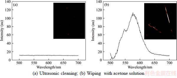
Figure 1 Fluorescence spectroscopy of dark-field microscopy images of samples:
2.2 Experimental apparatus
A confocal fluorescence microscope provides better fluorescence location discrimination than a wide-field microscope [24] because of greater attenuation of fluorescence sources outside the focal point [27]. Hence, the detected fluorescence decreases when the focal point is moved away from the source. A multi-channel confocal fluorescence microscope (Fluoromax-4, HORIBA Scientific) was used here to scan focal planes layer by layer at different depths along the z-axis.
Brittle fused silica samples had subsurface defects after lapping and polishing, and quantum dots added to the slurry were trapped in the subsurface to tag the position of subsurface defects in the dynamic processing. The SSD depth was determined by detecting changes in the fluorescence intensity at feature points or focal planes.
Taper polishing and spot MRF (Q22-400X, QED Technologies) were performed under the same conditions to verify the accuracy of the nondestructive detection method. The samples were analyzed with an optical microscope and a stylus profilometer (Talysurf PGI1240), equipped with a 2 ��m radius coni-spherical diamond stylus.
2.3 SSD depth detection
Under intense laser irradiation, an optical surface in the absence of quantum dots will produce broad background fluorescence that could adversely affect test results. Thus, an optical surface without quantum dots was firstly analyzed with the confocal fluorescence microscope. Quantum dot emissions below a certain intensity threshold were equivalent to black background fluorescence, emission higher that the threshold was considered to be from excitation of quantum dots. Fluorescence images obtained by before and after threshold processing are shown in Figure 2. The threshold processing was performed with MATLAB software. After threshold processing, the fluorescence intensity at each point was expressed as:
 (1)
(1)
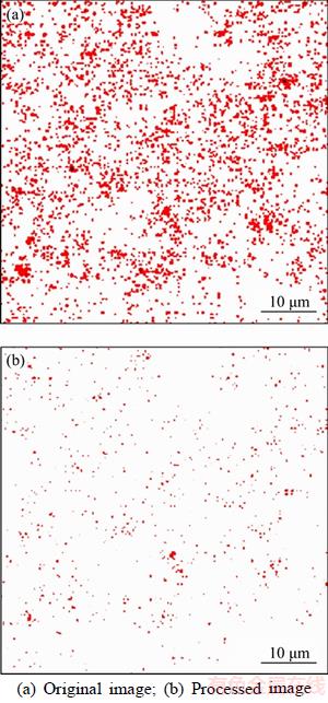
Figure 2 Confocal fluorescence images before and after threshold processing:
Fluorescence could still be observed at locations of high scattering intensity, but the signal in the image was weak and could be ignored. In addition, the confocal fluorescence microscopy was particularly sensitive to background light sources such as incandescent lamps and computer screens. Thus, the experiments were conducted in a darken room.
The major advantage of the slice scan is that fluorescence can be imaged at different depths. However, the fluorescence at a specific focal plane was not necessarily caused by excitation of quantum dots in the same focal plane and may be superposed by quantum dots in an adjacent focal plane. RUETTINGER et al [28] reported that the effective volume was not a perfect three- dimensional (3D) Gaussian, nor did it have rotational symmetry along the optical axis. All sections of the effective volume were fitted with a two-dimensional Gaussian function. However, the fluorescence from quantum dots was consistent with a 3D Gaussian distribution [29] given by:

 (2)
(2)
To determine the correspondence between fluorescence intensity and SSD depth in lapped optics, images were obtained at different focal depths, as shown in Figure 3.
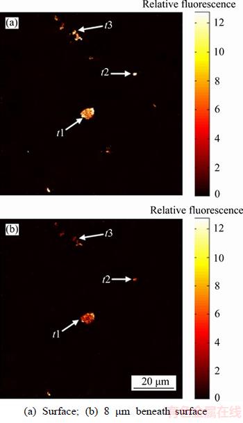
Figure 3 Fluorescence images of glass sample at different focal depths:
Gray values were exported by LAS AF Lite software. The maximum, minimum, and mean fluorescence intensities at different depths were derived. Relative changes in focal plane fluorescence intensity with depth are shown in Figure 4.
The results showed that the maximum fluorescence intensity was stable in the initial stage and then decreased at a critical scan depth, which was the SSD depth. According to the aforementioned model [28], relative fluorescence intensity at the confocal plane will diminish with increasing depth as shown in Figure 4(a), and the relative fluorescence intensity at a 6 ��m depth starts to decrease. Hence, SSD depth can be detected by the florescence method.
SSD could also be evaluated by changes in the relative fluorescence intensity at feature points t1, t2 and t3 as shown in Figure 4(b). The local depth for t1 was the largest, where the maximum relative fluorescence intensity decreased. Thus, the SSD depth was 6 ��m.
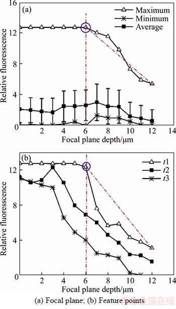
Figure 4 Relative fluorescence intensity with focal plane depth:
Samples were lapped with three sizes of cerium oxide slurries (W45, W28 and W14) under a load of 22 kPa, and with 40 r/min spindle speeds. The concentrations of slurry and quantum dots were 10 wt% and 0.005 mg/mL, respectively. The lapping time was 30 min.
2.4 Evaluation of fluorescence method
To assess the nondestructive method, taper polishing and spot MRF were performed under the same conditions. The subsurface damage depths generated by the W45, W28 and W14 abrasive grain sizes were characterized.
A polyurethane pad was used to finish taper polishing, which is described as follows. In the first step, three identical glasses at a certain angle were uniformly bonded on a loading block to ensure a uniform force. Then a slight angle was formed and sufficiently polished to remove SSD during lapping with cerium oxide solution for 3 h. In the next step, the samples were ultrasonically cleaned in anhydrous ethanol and etched in 5% HF acid for 10 min. After that, subsurface cracks were prone to open. In the last step, defect lengths in the three regions were measured with an optical microscope, and the polished angles were calibrated with a stylus profiler (see Figure 5). Finally, the SSD depth was calculated.
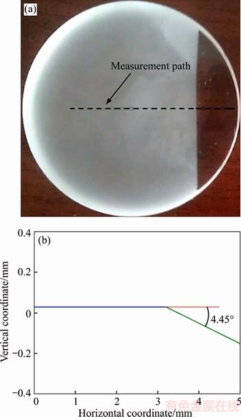
Figure 5 Calibration of fused silica optics by taper polishing
Lapping before MRF was the same as that before taper polishing. The concentration of MRF fluid with diamond powder was 14%, the flow rate of the polishing liquid was 1500 mL/min, the polishing wheel speed was 120 r/min, and the wheel was inclined at an angle, as shown in Figure 6. The samples were placed 5% HF etching solution for 5 min and surface impurities were removed ultrasonically. SSD depths were determined by comparing cross-section profiles.
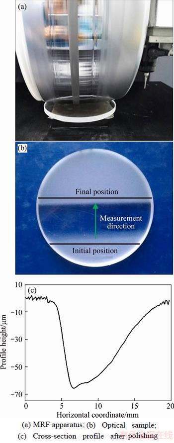
Figure 6 MRF apparatus and sample:
3 Results and discussion
3.1 Fluorescence intensity vs SSD depth
Fluorescence images of a sample lapped with W45 abrasive particles are shown in Figure 7. Two scan regions were selected to analyze the relative fluorescence intensity of feature points. Points with high fluorescence intensities were reference points. The distance between adjacent slices was 2.6 ��m.
The results indicated that quantum dots within the near-surface distance were uniformly embedded in subsurface defects. In region A (Figure 7(a)), the relative fluorescence intensity for feature points a1, a2 and a3 kept maximum values until the focal plane depths were 10.4, 7.8 and 18.2 ��m, respectively (Figure 7(b)), which were also the SSD depths.
Similarly, in region B (Figure 7(c)) for feature points b1, b2, and b3, the SSD depths were 18.2, 15.6 and 10.4 ��m respectively (Figure 7(d)). The test results revealed no apparent differences between the locations for a given sample. Subsurface defects were uniformly distributed, and the distances between adjacent slices were not small, and the SSD depth should be present between two adjacent slices. Therefore, the SSD depth generated by W45 abrasive particles was in the range of 18.2�C20.8 ��m.
Fluorescence images of samples lapped with W28 and W14 abrasive particles are shown in Figures 8 and 9. SSD depths were in the ranges of 11�C12 ��m for W28 abrasive particles and 8�C10 ��m for W14 abrasive particles.
3.2 Comparative analysis
Subsurface cracks caused by different sizes of abrasive particles had similar damage characteristics. A large number of cracks appeared on taper-polished surfaces. With increasing depth from the surface, overlapping shell-shaped cracks gradually disappeared. After reaching a certain depth, the crack density gradually decreased. Finally, SSD depths for the W45, W28 and W14 abrasive grain sizes were 26.7, 15.6 and 11.3 ��m, respectively. SSD morphologies at different depths after W45 taper polishing are shown in Figure 10.
Similarly, SSD depths after lapping with W45,W28 and W14 were determined by MRF polishing to be 25.2, 13.7 and 10.9 ��m, respectively. SSD morphologies at different depths after W45 MRF polishing are shown in Figure 11.

Figure 7 Relative fluorescence vs focal plane depth (b, d) at different regions (a, c) of sample surfaces lapped with W45 abrasive particles
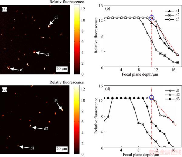
Figure 8 Relative fluorescence vs focal plane depth (b, d) for different regions (a, c) of sample surfaces lapped with W28 abrasive particles
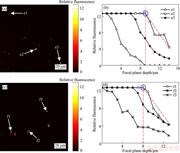
Figure 9 Relative fluorescence vs focal plane depth (b, d) for different regions (a, c) of sample surfaces lapped with W14 abrasive particles
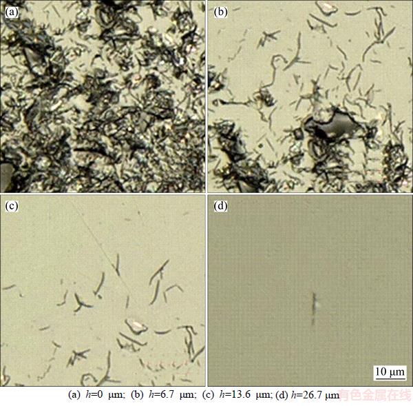
Figure 10 SSD morphologies of samples after W45 taper polishing:
All the experiments were performed with the same processing parameters. SSD depths determined by taper polishing, MRF, and fluorescent tagging are plotted in Figure 12.
The results revealed consistent data for the three methods regarding SSD vs abrasive grit size. Hence, nondestructive fluorescent tagging was effective for assessing SSD depths. Meanwhile, area ratios of cracks (crack densities) at different depths could be obtained from binary image processing, as shown in Figure 13. The results indicated that crack density decreases exponentially with depth.
Fluorescence detection results were smaller relative to the two destructive methods. This may be because the quantum dots were not completely embedded and trapped in subsurface defects. In addition, the test results were related to the number of analyzed regions. Generally, it was more likely to observe the maximum depth of SSD when more regions were analyzed.
Distributions of quantum dots at subsurface defects fell into three cases. In the first, the distributions were more uniform; thus, the relative fluorescence intensity was stable with increasing depth for a certain range. In the second case, subsurface crack density decreased with increasing depth, and the cracks disappeared at certain depths. Sporadic cracks appeared at deeper levels as marked by black circles in Figure 14. Because there were crack faults at certain depths, quantum dots were not fully embedded and trapped in the subsurface defects. Thus, there were detection errors that were a disadvantage of fluorescent tagging. Finally, if selected feature points, such as f3 in Figure 9(c), adhered to the sample surface, the relative fluorescence intensity decreased with increasing scan depth (Figure 9(b)). Hence, quantum dots may not have been completely removed from the sample surface during cleaning.
For optical glasses, LAMBROPOULOS [30] reported that SSD generally increased with increasing abrasive sizes up to 100 ��m, after which it reached a plateau. Therefore, the upper and lower bounds of SSD could be estimated from the abrasive size. Specifically, the SSD depth was bound according to the constrained inequality given in Eq. (3), where L is the abrasive size (��m). The lapping results here are in complete accord with this conclusion, and the relationship was fitted by an exponential function (Figure 12). If the power function was still applicable, the constraint relationship could be an inequality Eq. (4), according to the data. The effect of abrasive particles on SSD depth could be expressed by an exponential function, and the prediction range for SSD depth was reduced. This could give a priori guidance for processing damage for a given abrasive size.
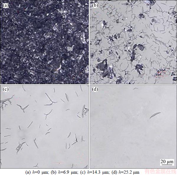
Figure 11 SSD morphologies of samples after W45 MRF polishing:
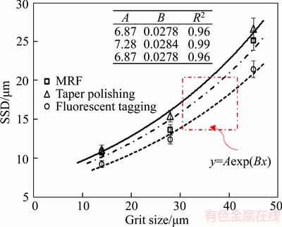
Figure 12 SSD vs grit size as determined by different methods
 (3)
(3)
 (4)
(4)
4 Conclusions
Subsurface defects in fused silica optics were fluorescently tagged by nanoscale quantum dots. The SSD depth could be determined by changes in the maximum relative fluorescence intensities both in the focal plane and at feature points. The scan depth was regarded as SSD depth when the relative fluorescence intensity decreased. Variations in relative fluorescence intensity vs focal plane depth were analyzed, and corresponding destructive detection experiments were performed under different processing conditions. The results indicated that nanoscale quantum dots were able to tag subsurface defects in optics. This effective non-destructive method has broad applications in detecting SSD in brittle optical materials.
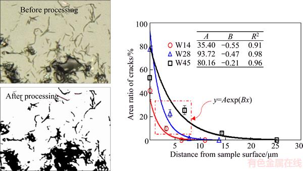
Figure 13 Area ratios of cracks based on binary surface images vs depth
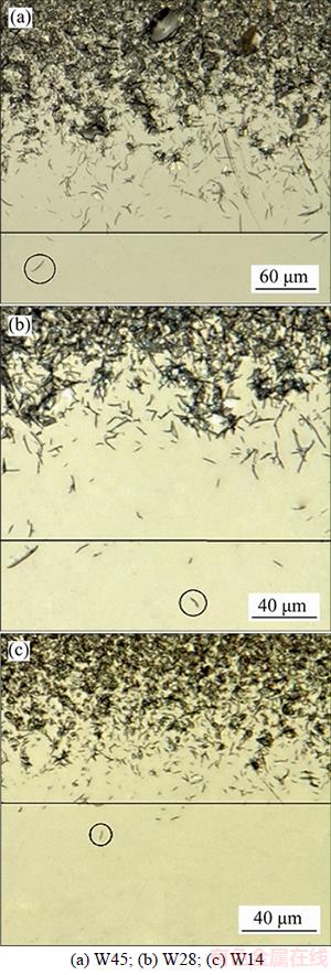
Figure 14 Defect topographies in fused silica optics induced by taper lapping:
References
[1] LI Hao-nan, YU Tian-biao, ZHU Li-da, WANG Wan-shan. Evaluation of grinding-induced subsurface damage in optical glass BK7 [J]. Journal of Materials Processing Technology, 2016, 229: 785�C794.
[2] BIFANO T G, FAWCETT S C. Specific grinding energy as an in-process control variable for ductile-regime grinding [J]. Precision Engineering�CJournal of the American Society for Precision Engineering, 1991, 13: 256�C262.
[3] BUIJS M, KORPELVANHOUTEN K. 3-body abrasion of brittle materials as studied by lapping [J]. Wear, 1993, 166: 237�C245.
[4] LI Sheng-yi, WANG Zhuo, WU Yu-lie. Relationship between subsurface damage and surface roughness of optical materials in grinding and lapping processes [J]. Journal of Materials Processing Technology, 2008, 205: 34�C41.
[5] ZHANG C, RENTSCH R, BRINKSMEIER E. Advances in micro ultrasonic assisted lapping of microstructures in hard-brittle materials: A brief review and outlook [J]. International Journal of Machine Tools & Manufacture, 2005, 45: 881�C890.
[6] LI Ya-guo, WU Yong-bo, WANG Jian, GUO Yin-biao, XU Qiao. Tentative investigation towards precision polishing of optical components with ultrasonically vibrating bound- abrasive pellets [J]. Optics Express, 2012, 20: 568�C575.
[7] LI Ya-guo, ZHENG Nan, LI Hai-bo, HOU Jing, LEI Xiang-yang, CHEN Xian-hua, YUAN Zhi-gang, GUO Zhao-zhou, WANG Jian, GUO Yin-biao, XU Qiao. Morphology and distribution of subsurface damage in optical fused silica parts: Bound-abrasive grinding [J]. Appl Surf Sci, 2011, 257: 2066�C2073.
[8] WILLIAMS W B, MULLANY B A, PARKER W C, MOYER P J, RANDLES M H. Using quantum dots to tag subsurface damage in lapped and polished glass samples [J]. Applied Optics, 2009, 48: 5155�C5163.
[9] BIFANO T G, DEPIERO D K, GOLINI D. Chemomechanical effects in ductile-regime machining of glass [J]. Precision Engineering�CJournal of the American Society for Precision Engineering, 1993, 15: 238�C247.
[10] BERCEGOL H, GRUA P, HEBERT D, MORREEUW J P. Progress in the understanding of fracture related laser damage of fused silica [C]// Proceedings of SPIE-The International for Optical Engineering. Boulder, CO, USA, 2007: 672003.
[11] Wang Chu, Wang Hong-xiang, Shen Lu, Hou Jing, Xu Qiao, WANG Jian, CHEN Xian-hua. Numerical simulation and experimental study on crack self-healing in BK7 glass [J]. Ceramics International, 2018, 44(2): 1850�C 1858.
[12] MILLER P E, BUDE J D, SURATWALA T I, SHEN N, LAURANCE T A, STEELE W A, MENAPACE J, FEIT M D, WONG L L. Fracture-induced subbandgap absorption as a precursor to optical damage on fused silica surfaces [J]. Opt Lett, 2010, 35: 2702�C2704.
[13] DONG Zhi-chao, CHENG Hao-bo , XU Ye, TAM H Y. Subsurface damage of fused silica lapped by fixed-abrasive diamond pellets [J]. Applied Optics, 2014, 53: 5841�C5849.
[14] Bian Yan-fei, ZHAI Wen-jie, Cheng Yuan-yuan, ZHU Bao-quan. Scratching by pad asperities in copper electrochemical-mechanical polishing [J]. Journal of Central South University, 2014, 21(11): 4157�C4162.
[15] Neauport J, Ambard C, Cormont P, Darbois N, Destribats J, Luitot C, Rondeau O. Subsurface damage measurement of ground fused silica parts by hf etching techniques [J]. Optics Express, 2009, 17: 20448�C20456.
[16] Hed P P, Edwards D F. Optical glass fabrication technology. 2: Relationship between surface roughness and subsurface damage [J]. Applied Optics, 1987, 26: 4677�C 4680.
[17] Menapace J A, Davis P J, Steele W A, Wong L L, Suratwala T I, Miller P E. MRF applications: Measurement of process-dependent subsurface damage in optical materials using the MRF wedge technique [R]. Livermore, CA: Lawrence Livermore National Laboratory (LLNL), 2005.
[18] Zhou Y Y, Funkenbusch P D, Quesnel D J, Golini D, Lindquist A. Effect of etching and imaging mode on the measurement of subsurface damage in microground optical-glasses [J]. J Am Ceram Soc, 1994, 77: 3277�C3280.
[19] Meeder M, Mauret T, Booij S M, Braat J J M, Faehnle O W. In Optimization of polishing processes by using itirm for in situ monitoring of surface quality [C]// Proceedings of SPIE-Optical Manufacturing and Testing V. Bellingham, WA, 2003, 5180: 40�C46.
[20] Ellingson W A, Todd J A, Sun J. Optical method and apparatus for detection of defects and microstructural changes in ceramics and ceramic coatings [P]. Google Patents: 2001.
[21] Neauport J, Cormont P, Legros P, Ambard C, Destribats J. Imaging subsurface damage of grinded fused silica optics by confocal fluorescence microscopy [J]. Optics Express, 2009, 17: 3543�C3554.
[22] Catrin R, Neauport J, Legros P, Taroux D, Corbineau T, Cormont P, Maunier C. Using sted and elsm confocal microscopy for a better knowledge of fused silica polished glass interface [J]. Optics Express, 2013, 21: 29769�C29779.
[23] WANG Zhuo, WANG Lin, YANG Jun-hong, PENG Wen-qiang, HU Hao. Detection of subsurface trace impurity in polished fused silica with biological method [J]. Optics Express, 2014, 22: 21292�C21301.
[24] Williams W, Mullany B, Parker W, Moyer P, Randles M. Using quantum dots to evaluate subsurface damage depths and formation mechanisms in glass [J]. CIRP Annals�CManufacturing Technology, 2010, 59: 569�C572.
[25] ZAN Feng, DONG Chao-qing, LIU Heng, REN Ji-cun. Experimental studies on blinking behavior of single Inp/Zns quantum dots: Effects of synthetic conditions and uv irradiation [J]. The Journal of Physical Chemistry C, 2012, 116: 3944�C3950.
[26] LIN Yi, XIE Hai-yan, ZHANG Zhi-ling, TIAN Zhi-quan, PANG Dai-wen. Fluorescent semiconductor quantum dots for biolabeling [J]. Progress in Chemistry 2007, 19: 1861�C1865.
[27] Hocken R J, Chakraborty N, Brown C. Optical metrology of surfaces [J]. CIRP Annals-Manufacturing Technology, 2005, 54: 169�C183.
[28] Ruttinger S, Buschmann V, Kr mer B, Erdmann R, Macdonald R, Koberling F. Comparison and accuracy of methods to determine the confocal volume for quantitative fluorescence correlation spectroscopy [J]. Journal of Microscopy, 2008, 232: 343�C352.
[29] Ruttinger S, Buschmann V, Kr mer B, Erdmann R, Macdonald R, Koberling F. In Determination of the confocal volume for quantitative fluorescence correlation spectroscopy [C]// Confocal, Multiphoton, and Nonlinear Microscopic Imaging III. Munich: Optical Society of America, 2007: 6612�C6630.
[30] Lambropoulos J. From abrasive size to subsurface damage in grinding [C]// Optical Fabrication and Testing. Qu��bec City: Optical Society of America, 2000: 17�C18.
(Edited by HE Yun-bin)
���ĵ���
ӫ�ⷨ������ѧԪ���DZ���������ȵ�ʵ���о�
ժҪ��������������ӫ�����ӵ�Թ�ѧԪ���DZ���ȱ�ݽ��б�ǣ����ù��۽�ӫ�������Ծ۽�����������ɨ�裬�õ�������Ʒ��ͬ��ȴ�����Ƭͼ��ͨ��������ӫ��ǿ�ȵı仯��������������ʯӢ��ѧԪ�����DZ���������ȡ������������ɨ����ȳ����ٽ�ֵʱ�����ӫ��ǿ�ȼ����½�����ѧԪ���DZ���������ȿ���ͨ�����ӵ�ʵ��Ƕ�����ȷ�������ǵ��ƻ��Լ�ⷽ������Ч��֤�������ⷽ�����Ƕ��⡢��������ʵ������ͬ�������½��С�����������������ӵ�Թ�ѧԪ���ı���ȱ�ݾ������õı�ע���������⣬�����ⷽ��������Ч��������ʯӢԪ�����DZ���������ȡ�
�ؼ��ʣ���ѧԪ�����DZ���ȱ�ݣ������⣻��ĥ���DZ�������
Foundation item: Project(JCKY2016212A506-0503) supported by the Science Challenge Project of China; Project(51475106) supported by the National Natural Science Foundation of China
Received date: 2017-03-27; Accepted date: 2017-07-18
Corresponding author: WANG Hong-xiang, PhD, Professor; Tel: +86�C451�C86413802; E-mail: whx@hit.edu.cn; ORCID: 0000-0001- 7534-8341