Trans. Nonferrous Met. Soc. China 23(2013) 3629-3633
Growing process and reaction mechanism of electroless Ni-Mo-P film on SiO2 substrate
Mei-ling WANG1,2, Zhi-gang YANG1, Chi ZHANG1, Dian-long LIU1
1. School of Materials Science and Engineering, Tsinghua University, Beijing 100084, China;
2. Division of Nano Metrology and Materials Measurement, National Institute of Metrology, Beijing 100013, China
Received 14 March 2013; accepted 10 September 2013
Abstract: The diffusion barrier Ni-Mo-P film for Cu interconnects was prepared on SiO2/Si substrate using electroless method. The surface morphology and composition during the formation process of electroless Ni-Mo-P film were investigated through analyzing samples of different deposition time. Induced nucleation, induced co-deposition, and self-induced growth mechanisms involved in electroless process were confirmed by field-emission scanning electron microscopy (FE-SEM), energy dispersive spectrometry and atomic force microscopy (AFM). Firstly, the preceding palladium particles as catalysts induce the nucleation of nickel. Secondly, the nickel particles induce the deposition of molybdenum and phosphorus, which attributes to induced co-deposition. Thirdly, former deposited Ni-Mo-P induces deposition of the latter Ni-Mo-P particles. Moreover, the reaction mechanism was proposed with the oxydate of  .
.
Key words: Ni-Mo-P deposit; induced-deposition; electroless deposition; SiO2 substrate
1 Introduction
Copper has been widely used instead of aluminum in ultra-large scale integration (ULSI) technology for integrated circuit (IC) owing to its lower electrical resistance and higher electromigration resistance [1-6]. However, the interdiffusion between Cu and SiO2 would likely happen when the temperature reached 473 K [7,8]. Moreover, the adhesion between Cu and SiO2 substrate is weak [9,10]. So, a diffusion barrier between Cu and SiO2/Si substrate should be formed to prevent the diffusion of Cu atoms into the substrate and meanwhile to improve the adhesion between Cu and substrate. In order to employ a simple procedure, reduce the cost of process, and obtain the good step coverage with nano-scale trenches and vias, electroless deposition of diffusion barrier has been of great interest [1-11]. PAUNOVIC et al [12] prepared Ni-P, Co-P coatings using electroless deposition. They found that coatings with high P content exhibited amorphous state thus were effective to prevent interdiffusion between Cu and Si. However, Ni-P and Co-P coatings had bad thermal stability. Therefore, Mo and W were considered to improve thermal stability of coating. KOHN et al [13] studied Co-W-P and Co-Mo-P coatings as barrier layers. They found that the maximum content of W was 11% (mole fraction), while Mo content was only 2.7% (mole fraction). OSAKA et al [14,15] deposited Ni-B, Ni-W-B and Ni-Re-P coatings and investigated barrier property, composition, and thermal stability of coatings. CHANG [16] electrodeposited the Ni-W-P coatings. He adjusted pH value, concentration of Na2WO4, temperature of solution to control the property of coatings. WU et al [17] deposited Ni-Mo-P films on SiO2 substrate and assessed the barrier property of Ni-Mo-P films. The results showed excellent barrier properties after 400 °C annealing for 1 h. LIU et al [11] used PdCl2 activation and self-assembly method to deposit Ni-Mo-P film directly on SiO2 substrate without any seed layer successfully. Among varies of ternary alloy coatings, Ni-Mo-P exhibited outstanding barrier properties thus should receive more attention. But few reports explain the formation process of Ni-Mo-P film in details with corresponding experimental results. In this work, the forming process of Ni-Mo-P was studied experimentally. The morphology transformation of electroless Ni-Mo-P films on SiO2 as a function of deposition time was investigated, and the mechanism of the nucleation and growth of Ni-Mo-P films by electroless deposition on SiO2 was studied.
2 Experimental
(100)-oriented Si wafers, coated with 250 nm-thick thermal oxide (SiO2) layers, were used as the substrates. The pretreatment process of substrates included the cleaning, coupling and activation stage. Cleaning solution included acetone, 10% HCl, deionized water chronologically. 3-ammonium propyl silane three oxygen radicals and PdCl2 were used as coupling agent and activation agent, respectively. The electroless plating bath composition was 25 g/L NiSO4・6H2O, 0.34 g/L Na2MoO4・2H2O, 20 g/L NaH2PO2・H2O, 25 g/L Na3C6H5O7・2H2O, 2.1 g/L acetic acid, 0.004 g/L NH4F, and 0.008 g/L sodium dodecyl sulfate. The pH value and bath temperature were 11.5 and 80-90 °C, respectively. The deposition time was 1-60 s from the beginning of deposition.
The surface morphology of Ni-Mo-P films was investigated by field emission scanning electron microscopy (FE-SEM), and the composition of deposits was detected by energy dispersive spectrometry (EDS). Atomic force microscopy (AFM) was used to observe the three-dimensional microstructures of Ni-Mo-P deposits.
3 Results and discussion
3.1 Forming process of Ni-Mo-P deposit
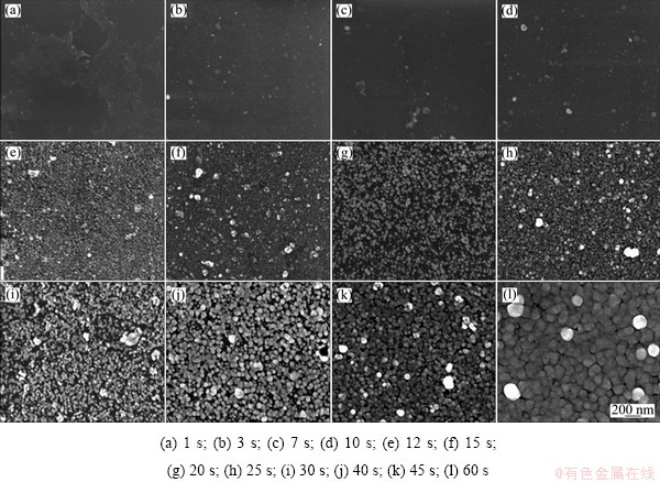
Figure 1 shows a series of FE-SEM images of the electroless Ni-Mo-P deposited at different time. It can be seen from Fig. 1 that when the deposition process went on, the deposit layer gradually became more continuous and uniform. Additionally, both the thickness and granule size of the electroless Ni-Mo-P alloy on substrate increased.
Figure 1(a) shows the surface image of the electroless Ni-Mo-P alloy deposited for 1 s after the beginning of the deposition, where an incontinuous and semi-bright monolayer on the SiO2 surface can be clearly observed. This semi-bright monolayer consisted of Pd granules according to the EDS results, no Ni, Mo, or P element was detected. However, such monolayer of the electroless Ni-Mo-P alloy cannot be observed after 3 s deposition, as shown in Fig. 1(b), where fine granules spread all over the surface. Based on the EDS analysis, although the semi-bright monolayer disappeared, palladium could be detected on the surface and it still showed no trace of the elements of nickel, molybdenum and phosphorus. Figure 1(c) illustrates that after initiation for 7 s, some large particles distributed on the surface randomly, which contained palladium and nickel according to the elemental analysis. Other areas without these large particles only showed signs of silicon and oxygen as contended in the substrate. Such large particles may have formed due to the agglomeration of fine palladium nanoparticles followed by the deposition of nickel. In addition, it also revealed that nickel was more likely to deposit around the palladium particles rather than precipitate on the blank substrate sites in the early stages of electroless Ni-Mo-P deposition process in order to achieve a minimum total surface energy [18]. It can be seen that in Fig. 1(d), after 10 s initiation, the granule size was slightly increased and some fine granules were uniformly distributed on the surface. However, according to the elemental analysis results, only palladium and nickel as well as the elements in the substrate were detected on the surface. A bright surface with fine granules appeared as shown in Fig. 1(e) after 12 s initiation, and the density of these fine granules increased dramatically. Moreover, all of the nickel, molybdenum and phosphorus were detected after 15 s initiation as shown in Fig. 1(f), and more large particles with size of 50-200 nm appeared compared with Fig. 1(e). As shown in Fig. 1(g), the surface of the electroless Ni-Mo-P alloy deposited for 20 s was covered by uniform spherical granules with the size of 30-40 nm. As shown in Fig. 1(h), the granule size increased slightly and the density of electroless deposits increased evidently compared with Fig. 1(g). After 30 s initiation (see Fig. 1(i)), the adjacent granules began to connect and form aggregations after 40 s initiation (see Fig. 1(j)), and the granules grew and presented uniform spherical shape. As shown in Fig. 1(k), the surface density of electroless Ni-Mo-P alloy deposited for 45 s increased as expected. When the deposition time reached 60 s, as shown in Fig. 1l, a uniform and dense Ni-Mo-P layer with bulky particles formed completely.

Fig. 1 FE-SEM images of electroless Ni-Mo-P deposited for different time
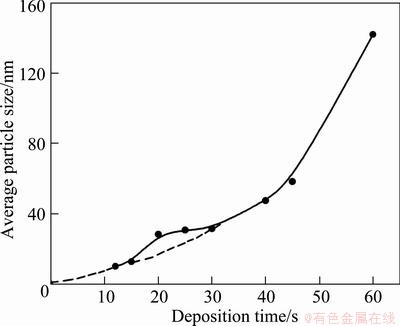
Figure 2 shows the average granule size of electroless Ni-Mo-P deposits as a function of deposition time. As shown in Fig. 2, the average granule size basically showed exponential increase trend. The granule size increased slowly during deposition time from 20 to 30 s. After 30 s, the granule size increased significantly.

Fig. 2 Average granule size of deposits as function of deposition time
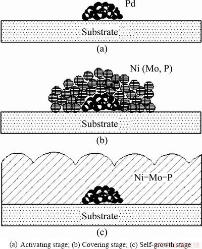
Based on the changes of surface morphology and composition, the formation process of continuous Ni-Mo-P film on SiO2 substrate can be divided into three stages: activating stage, covering stage, self-growth stage. The schematic illustration is shown in Fig. 3. In the initial stage the Pd2+ ions adsorbed on the substrate were reduced firstly, and other ions in the solution could not accomplish mass transformation and adsorption process within so short time although they were also reduced. Therefore, there was only palladium deposited on the surface. Subsequently, the covering stage started and nickel deposited at the activated sites around Pd atoms. Molybdenum and phosphorus also co-deposited with nickel on the surface simultaneously. Elemental analysis results of Figs. 1(c-e) indicated that the deposition of nickel was prior to the deposition of molybdenum and phosphorus, which was accordance with the induced co-deposition theory [19]. As the deposition process carried on, the palladium would eventually be covered entirely by electroless Ni-Mo-P deposits. After that, the deposition process entered into the self-growth stage, and the surface density and granule size would increase with deposition time. From Fig. 1, it can be observed that the deposited granules in different stages typically formed in a round shape to reduce the surface energy and keep stable.

Fig. 3 Schematic illustration of formation process stages
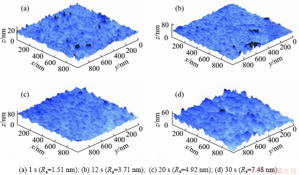
AFM was used to demonstrate the deposition process of Ni-Mo-P film directly. Figure 4 shows the three-dimensional AFM surface morphology of Ni-Mo-P deposits at different deposition time. The corresponding surface roughnesses (Ra) are 1.51, 3.71, 4.92 and 7.48 nm, approximately. The increase of surface roughness with deposition time attributes to the growth of Ni-Mo-P granules.

Fig. 4 Three-dimensional AFM images of Ni-Mo-P deposits at different deposition time
3.2 Reaction mechanism of Ni-Mo-P deposits
Generally, electroless deposition consists of series of redox reactions. A strong reducing agent was used to reduce metal ions to metal which is deposited on surface of materials to form a dense coating [19,20]. In this work,  , as the reducing agent, is oxidized to release electrons in the reaction process. The electrons are involved in reduction reactions of Ni, Mo and P. Since it is very short for the reactions, much reducing agent (
 ) is probably left. Moreover, the pH value of reaction solution is 11.0 which means the concentration of OH- is high. Moreover, the existence of oxydate
  is confirmed by ion chromatograph with the P concentration of 1.52 g/L. So the reaction showed by formula (1) is most likely the main oxidation reaction.
 (1)
(1)
The reduction reactions are as follows [21,22]:
 (2)
(2)
 (3)
(3)
 (4)
(4)

 (5)
(5)

 (6)
(6)
where L in formula (5) and (6) represents a ligand.
4 Conclusions
1) The surface morphology and composition during the formation process of electroless Ni-Mo-P film was confirmed. Pd, Ni, Mo and P were all detected on the surface.
2) The nucleation and growth of Ni-Mo-P films by electroless deposition include three stages: First, the preceding palladium granules induce the nucleation of nickel as catalyst centers; Second, the nickel granules induce the deposition of molybdenum and phosphorus, which attributes to ‘induced co-deposition’; Third, the former deposited Ni-Mo-P induces the deposition of the latter Ni-Mo-P, which is called ‘self-induced deposition’. The average granule sizes basically show exponential increase trend.
3) The reaction mechanism of electroless Ni-Mo-P film was studied. It is indicated that the oxydate of  in alkaline solution is
  .
.
References
[1] ANUJ K, MUKWSH K, DINESH K. Effect of composition on electroless deposited Ni-Co-P alloy thin films as a diffusion barrier for copper metallization [J]. Applied Surface Science, 2012, 258: 7962-7967.
[2] ANUJ K, MUKWSH K, DINESH K. Deposition and characterization of electroless Ni-Co-P alloy for diffusion barrier applications [J]. Microelectronic Engineering, 2010, 87: 387-390.
[3] FANG J S, LIN J H, CHEN B Y, CHEN G S, CHIN T S. Low-resistivity Ru-Ta-C barriers for Cu interconnects [J]. Journal of Electronic Materials, 2012, 41(1): 138-143.
[4] LUO Hong-jie, SONG Bin-na, LIU Yi-han, YAO Guang-chun. Electroless Ni-P plating on Mg-Li alloy by two-step method [J]. Transactions of Nonferrous Metals Society of China, 2011, 21(10): 2225-2230.
[5] LIU Hong, GUO Rong-xin, LIU Zhu. Characteristics of microstructure and performance of laser-treated electroless Ni-P/Ni-W-P duplex coatings [J]. Transactions of Nonferrous Metals Society of China, 2012, 22(12): 3012-3020.
[6] YOSHINO M, MASUDA T, YOKOSHIMA T, SASANO J, SHACHAM-DIAMAND Y, MATSUDA I, OSAKA T, HAGIWARA Y, SATO I. Electroless diffusion barrier process using SAM on low-k dielectrics [J]. Journal of the Electrochemical Society, 2007, 154(3): D122-D125.
[7] WANG Zeng-lin, SAKAUE H, SHINGUBARA S, TAKAHAGI T. Influence of surface oxide of sputtered TaN on displacement plating of Cu [J]. Japanese Journal of Applied Physics B, 2003, 42(4): 1843-1846.
[8] JIA Yan-hui. The diffusion and interface reaction of Cu/Si(100) system [D]. Lanzhou: Lanzhou University, 2009. (in Chinese)
[9] INOUE F, SHIMIZU T, YOKOYAMA T, MIYAKE H, KONDO K, SAITO T, HAYASHI T, TANAKA S, TERUI T, SHINGUBARA S. Formation of electroless barrier and seed layers in a high aspect ratio through-Si vias using Au nanoparticle catalyst for all-wet Cu filling technology [J]. Electrochimica Acta, 2011, 56(17): 6245-6250.
[10] LIU B T, CHEN J H, LI X H, WANG K M, LI M, ZHAO D Y, YANG L, ZHAO Q X, MA L X, ZHANG X Y. Investigation of amorphous Ni-Al-N film as diffusion barrier between Cu and SiO2 [J]. Journal of Alloys and Compounds, 2011, 509: 8093-8096.
[11] LIU Dian-long, YANG Zhi-gang, ZHANG Chi. Electroless Ni-Mo-P diffusion barriers with Pd-activated self-assembled monolayer on SiO2 [J]. Materials Science and Engineering B, 2010, 166(1): 67-75.
[12] PAUNOVIC M, BAILEY P J, SCHAD R G, SMITH D A. Electrochemically deposited diffusion barriers [J]. Journal of Electrochemical Society, 1994, 141(7): 1843-1850.
[13] KOHN A, EIZENBERG M, SHACHAM-DIAMAND Y, SVERDLOV Y. Characterization of electroless deposited Co(W, P) thin films for encapsulation of copper metallization [J]. Materials Science and Engineering A, 2001, 302: 18-25.
[14] OSAKA T, TAKANO N, KUROKAWA T, UENO K. Fabrication of electroless NiReP barrier layer on SiO2 without sputtered seed layer [J]. Electrochemical and Solid-State Letters, 2002, 5(1): 7-10.
[15] OSAKA T, TAKANO N, KUROKAWA T, KANEKO T, UENO K. Characterization of chemically-deposited NiB and NiWB thin films as a capping layer for ULSI application [J]. Surface and Coatings Technology, 2003, 169: 124-127.
[16] CHANG S Y. Electroless deposition of NiWP film as diffusion barrier for Cu interconnects [D]. HSINCHU, Taiwan: National Tsinghua University, 2004: 76-77.
[17] WU Y, WAN C C, WANG Y Y. Fabrication of potential NiMoP diffusion barrier/seed layers for Cu inter-connects via electroless deposition [J]. Journal of Electronic Materials, 2005, 34(5): 541-550.
[18] CHANG Shou-yi, HSU Chia-jung, FANG Ray-hua, LIN Su-jien. Electrochemical deposition of nanoscaled palladium catalysts for 65nm copper metallization [J]. Journal of the Electrochemical Society C, 2003, 150(9): C603-C607.
[19] YOSHINO M, NONAKA Y, SASANO J, MATSUDA I, SHACHAM-DIAMANDY, OSAKA T. All-wet fabrication process for ULSI interconnect technologies [J]. Electrochimica Acta, 2005, 51(5): 916-920.
[20] JIANG Xiao-xia, SHEN Wei. The theory and application of electroless deposition [M]. Beijing: National Defence Industry Press, 2000. (in Chinese)
[21] CHOU Yu-hsien, SUNG Yuh, BAI Ching-yuan, GER Ming-der. Effects of molybdate concentration on the characteristics of Ni-Mo-P diffusion barriers grown by nonisothermal electroless deposition [J]. Journal of the Electrochemical Society, 2008, 155 (9): D551-D557.
[22] CHOU Yu-hsien, SUNG Yu, LIU Yih-ming, PU Nen-wen, GER Ming-der. Amorphous Ni-Mo-P diffusion barrier deposited by non-isothermal deposition [J]. Surface and Coatings Technology. 2009, 203(8): 1020-1026.
SiO2基底上化学镀Ni-Mo-P薄膜的生长和形成机理
王梅玲1,2,杨志刚1,张 弛1,刘殿龙1
1. 清华大学 材料学院,北京 100084;
2. 中国计量科学研究院 纳米新材料所,北京 100013
摘 要:采用化学镀方法在SiO2/Si 基底上制备Cu互联线用阻挡层材料Ni-Mo-P薄膜。采用场发射扫描电子显微镜、电子分散能谱仪、原子力显微镜分析不同沉积时间样品的表面形貌和成分,并对Ni-Mo-P薄膜的形成过程进行研究。Ni-Mo-P薄膜的形成过程分为3个阶段:催化阶段,先前还原的Pd颗粒成为Ni还原的催化形核中心,诱导Ni沉积;覆盖阶段,Ni颗粒诱导Mo、P与之进行共沉积;自生长阶段,Ni-Mo-P薄膜共同沉积,颗粒生长。阐述了还原剂被氧化后产物为 的的反应机理。
关键词:Ni-Mo-P镀层;诱导沉积;化学镀;SiO2基底
(Edited by Xiang-qun LI)
Corresponding author: Zhi-gang YANG; Tel: +86-10-62795031; E-mail: zgyang@tsinghua.edu.cn
DOI: 10.1016/S1003-6326(13)62910-6