�ǶԳƽṹCu/Sn-58Bi/Cu������ ��Ǩ������֯�ݱ估����
��Դ�ڿ����й���ɫ����ѧ��(Ӣ�İ�)2014���5��
�������ߣ��� �� �غ첨 ������ �� �� ����ƽ
����ҳ�룺1619 - 1628
�ؼ��ʣ������裻�ǶԳƺ��㣻��Ǩ��Σ��������ӵ������״ЧӦ
Key words��microregional electrical resistance; asymmetric solder interconnect; electromigration damage; current crowding; geometry effect
ժ Ҫ������ԭλSEM�۲졢FIB������������Ԫ(FE)ģ���о��˷ǶԳƽṹCu/Sn-58Bi/Cu �����е�Ǩ���������֯�ݱ估�����ˡ�����������ǶԳƽṹ�����и�Bi��ƫ�ۺ����Ƶȵ�Ǩ������Զ�ȶԳƺ��������أ�FIB-SEM�۷��������ʾ�ǶԳƺ������ص��������ϸ������ڵ�������ǵ��º�������ϵ����Ǿ��ȷֲ������ص�Ǩ������Ĺؼ����أ����۷�����ģ��������������ӵ���������ں������������С��λ�á�
Abstract: The electromigration induced microstructure evolution and damage in asymmetric Cu/Sn-58Bi/Cu solder interconnects were investigated by in-situ SEM observation, focused ion beam (FIB) microanalysis and finite element (FE) simulation. The SEM results show that the electromigration-induced local degradation of microstructures, i.e., segregation of Bi-rich phase and formation of microcracks, in the asymmetric solder interconnects is much severer than that in the symmetrical ones. FIB-SEM microanalysis reveals that the microregional heterogeneity in electrical resistance along different electron flowing paths is the key factor leading to non-uniform current distribution and the resultant electromigration damage. Theoretical analysis and FE simulation results manifest that the current crowding easily occurs at the local part with smaller resistance in an asymmetric solder interconnect. All results indicate that the asymmetric shape of the solder interconnect brings about the difference of the electrical resistance between the different microregions and further results in the severe electromigration damage.
Trans. Nonferrous Met. Soc. China 24(2014) 1619-1628
Wu YUE, Hong-bo QIN, Min-bo ZHOU, Xiao MA, Xin-ping ZHANG
School of Materials Science and Engineering, South China University of Technology, Guangzhou 510640, China
Received 26 September 2013; accepted 3 December 2013
Abstract: The electromigration induced microstructure evolution and damage in asymmetric Cu/Sn-58Bi/Cu solder interconnects were investigated by in-situ SEM observation, focused ion beam (FIB) microanalysis and finite element (FE) simulation. The SEM results show that the electromigration-induced local degradation of microstructures, i.e., segregation of Bi-rich phase and formation of microcracks, in the asymmetric solder interconnects is much severer than that in the symmetrical ones. FIB-SEM microanalysis reveals that the microregional heterogeneity in electrical resistance along different electron flowing paths is the key factor leading to non-uniform current distribution and the resultant electromigration damage. Theoretical analysis and FE simulation results manifest that the current crowding easily occurs at the local part with smaller resistance in an asymmetric solder interconnect. All results indicate that the asymmetric shape of the solder interconnect brings about the difference of the electrical resistance between the different microregions and further results in the severe electromigration damage.
Key words: microregional electrical resistance; asymmetric solder interconnect; electromigration damage; current crowding; geometry effect
1 Introduction
With the continuous pursuit of the portability and miniaturization of electronic devices and products, the packing density is increasing and the dimension of solder interconnects is scaling down. Accordingly, the current density in solder interconnects gets higher and higher, easily leading to electromigration (EM) [1-3] and the resultant severe electromigration-related structural problems, such as microstructure coarsening, intermetallic compound (IMC) polarity or abnormal polarity growth, whiskers, hillocks and voids. These structural problems and defects will deteriorate the reliability of the solder interconnect, therefore, electromigration has been regarded as a serious reliability issue. Previous studies showed that electromigration-induced damage was related to many factors [2, 3], such as compositions of the solder, under bump metallization (UBM), current stressing condition and operating temperature. Thus far, however, most studies were focused on electromigration in flip chip (FC) solder joints [4-9] and the results revealed that the current crowding effect at the enter window is the key factor leading to electromigration, which is formed in the redistributing course of the electron flow from line to bump. Many methods were proposed to reduce the electromigration-induced damage in FC solder interconnects [9-12], for instance, changing the solder composition, optimizing the passivation opening and UBM thickness. In fact, other types of solder interconnect structures are also used in electronic packages. For example, the right-angle interconnect is used to connect the three dimensional (3D) sensor and the substrate [13]. However, little is known about the electromigration behavior of these solder interconnects with asymmetric geometry. In our previous studies [14, 15], by comparatively investigating the electromigration behavior and microstructural evolution in the right-angle type and line-type Cu/Sn-3.0Ag-0.5Cu/Cu and Cu/ Sn-58Bi/Cu solder interconnects, it was qualitatively revealed that the heterogeneity in microregional distribution of electrical resistance along the electron flowing paths caused by the solder interconnect shape can result in the current crowding and consequently electromigration-induced damage. In this study, we aim to clarify the relation between the microregional current density and the corresponding resistance, and seek to establish an analytical equation to quantitatively explain the un-uniform electromigration behavior in the asymmetric solder interconnect, correspondingly, the right-angle and line-type solder joints were selected to comparatively investigate. In addition, three-dimensional (3D) finite element (FE) model was employed to simulate the distribution of current density in the right-angle solder joint.
2 Experimental
The solder interconnect samples were prepared by the following procedure: firstly, the commercial pure copper foil (99.9% purity) with a thickness of 150 ��m was cut into narrow ribbons with a width of 8 mm and a length of 20 mm; then the ends of the copper ribbons were mechanically ground with waterproof sandpapers of different grits in succession and polished with 0.05 ��m Al2O3 suspension; afterwards, the ribbons were ultrasonically cleaned in ethanol. The solder interconnect samples were assembled using the eutectic Sn-58Bi solder on a specially designed fixture by modeling reflow soldering process at 190 ��C with a dwelling time of 60 s and then cooled in air. After soldering, the Cu/Sn-58Bi/Cu interconnect samples were machined to U-shape, soldered trace line, and then embedded into the epoxy; finally, the embedded interconnect samples were carefully machined and polished to the final geometrical dimension shown in Fig. 1. These procedures were detailed in our previous works [14,15]. The electromigration tests were conducted at constant temperature (25 ��C) and humidity (60%) in a cleaning room, and the direct current (DC) density was 1.5��104 A/cm2. In order to observe the locally entire segregation of Bi-rich and Sn-rich phases, the stressing time was prolonged to 288 h in this study. Since the whole observation section (including copper wires) of the solder interconnect was opened, the heating dissipation was good and the temperature induced by the Joule heating was close to nil and could be neglected. The microstructural evolution of the solder joints for different current stressing time was characterized by a scanning electron microscope (SEM, Supra 55) equipped with an energy dispersive X-ray spectroscope (EDX, Oxford-7659). The phase segregation at the different inner microregions in both types of solder joints was investigated through cross-sectional analysis of the joints based on focused ion beam (FIB, SMI 3050MS2) and SEM. In order to obtain reliable experimental results, the tests were carried twice on three samples each time.
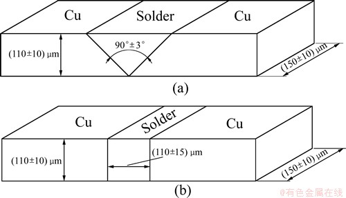
Fig. 1 Schematic sketch of right-angle type (a) and line-type (b) solder interconnects
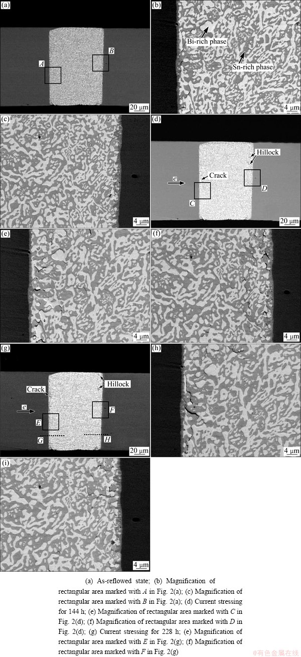
Fig. 2 In-situ BSE images of line-type Cu/Sn-58Bi/Cu solder interconnect in as-reflowed state and after current stressing for different periods
3 Results and discussion
3.1 Electromigration-induced morphology and micro- structure changes in right-angle type and line- type solder interconnects
Figures 2 and 3 show microstructure evolution of line-type and right-angle type interconnects respectively after current stressing for different periods, where the arrow with symbol ��e�� indicates the current direction, from the left to the right. Clearly, the initial microstructure features of both types of the interconnects in the as-reflowed state, as shown in Figs. 2(a)-(c) and 3(a)-(b), are similar, namely, the Sn-rich phase (dark contrast) and Bi-rich phase (bright contrast) distribute randomly and uniformly in the solder matrix of the interconnects. A thin layer of Cu6Sn5 confirmed by EDX analysis, with a thickness of about 1.8 ��m, formed at both interfaces of two types of the interconnects.
Figures 2(d)-(f) and 3(c)-(d) are in-situ backscattered electron (BSE) images of the microstructure of the interconnects corresponding to Figs. 2(a)-(c) and 3(a)-(b) respectively after current stressing for 144 h. A close comparison shows that some electromigration characteristics in both types of the interconnects are similar, namely, the Sn-rich and Bi-rich phases became coarse, hillocks occurred near the anode and cracks formed near the cathode. However, the thickness of the IMC layers at both the cathode and anode interfaces seems to show negligible change. In the meantime, Bi-rich phase congregated near the anode interface, indicating that Bi atom is the main diffusing species in Cu/Sn-58Bi/Cu interconnects during current stressing. This result is in good coincidence with that obtained in other studies [16,17]. Whereas, there are also some different electromigration behaviors between two types of solder interconnects. The electromigration- induced morphological changes in the right-angle interconnect, i.e., the hillocks at the anode and the cracks at the cathode, are much severer than those in the line-type one. In particular, it can be seen that the electromigration-induced hillocks and cracks distribute uniformly along the whole interface in the line-type interconnect, as shown in Figs. 2(e)-(f), while become severer and severer along the interface from the top side to the bottom corner in the right-angle type one, as shown in Figs. 3(c)-(d). It is worth noticing that the severest cracking problem occurs at the bottom corner of the right-angle type interconnect as shown in Fig. 3(d), indicating that this position is the weakest part during current stressing. Obviously, the electromigration- induced damage is much severer in the right-angle type interconnect with the asymmetric shape than in the line-type interconnect with the symmetrical shape.
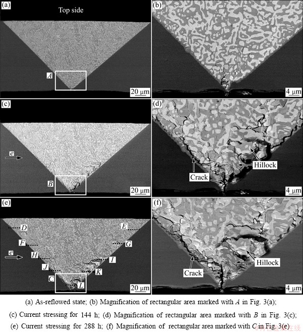
Fig. 3 In-situ BSE images of right-angle type Cu/Sn-58Bi/Cu interconnect in as-reflowed state and after current stressing for different periods
Furthermore, after current stressing for 288 h, the microstructure of both types of interconnects changed significantly, as shown in Figs. 2(g)-(i) and Figs. 3(e)- (f), where the hillocks grew, both Sn-rich and Bi-rich phases coarsened, and the cracks propagated continuously. However, the thickness of the IMC layer seems unchanged. By comparing the BSE images in Figs. 3(c)-(d) for electromigration of 144 h and the ones in Figs. 3(e)-(f) for electromigration of 288 h, it can be seen clearly that after a relatively long time current stressing, the main crack initiated at the bottom corner of the right-angle type joint and propagated along the cathode interface, whose length took up almost half of the whole interface length, and the hillocks and Bi congregation also developed continuously, as shown in Figs. 3(e)-(f).
In general, the diffusing atoms may migrate along grain boundaries, interfaces or surfaces in a polycrystalline alloy. The study on the electromigration behavior in SnPb solder strips showed that the interface between Sn and Pb phases served as the fastest kinetic path [18] and another work indicated that the eutectic Sn-58Bi solder exhibited similar electromigration characteristics to eutectic Sn-Pb alloy [19]. Thus, in the Cu/Sn-58Bi/Cu system, the Bi atoms will mainly migrate along the interface between Sn-rich and Bi-rich phases and congregate in front of the anode under current stressing. As described above, the electromigration characteristics between two types of solder interconnects are different, that is, the hillocking and cracking problems at the bottom corner of the right-angle type joint are much severer. Therefore, it is necessary to further investigate the internal microstructure evolution and mechanism of the electromigration behavior in both types of solder interconnects, in particular, the root cause leading to the big difference in the electromigration feature. Figures 4 and 5 show the cross-sectional FIB-BSE images of different positions at the cathode and anode interfaces of two types of the interconnects after current stressing for 288 h, which are corresponding to the positions marked with capital letters in Fig. 2(g) and Fig. 3(e), respectively.
Clearly, the internal morphology and microstructural characteristics of two types of the interconnects shown in Figs. 4 and 5 are different from those corresponding to the surface shown in Figs. 2 and 3. For example, the sizes of both Sn-rich and Bi-rich phases in the inner part of the interconnects are larger than those on the surface, indicating that the phase congregation and coarsening behavior in the inner part of the interconnects are severer, and the dimension of Bi-rich phase along the electron flow direction is larger than that in the vertical direction in the matrix of the solder. Because Sn is easily oxidized in air, a thin oxide-film may form on surface of the solder interconnect, which can impede the migration of the atoms to some extent. Further, the anisotropic resistivity of ��-Sn phase can induce the grain rotation under current stressing as indicated by some previous studies [20-22]. Therefore, under the combined effect of the above factors, the electromigration-induced morphology change and microstructure damage in the inner part of the interconnects are much severer than those in the superficial region.
It is worth noting that the segregation between Bi-rich and Sn-rich phases occurred significantly in the matrix of the solder at the bottom corner of the right-angle type interconnect after current stressing for 288 h, as shown in Fig. 5(i), but hardly took place in the line-type interconnect as shown in Fig. 4. Further, the electromigration characteristics at different positions of the right-angle type solder interconnect are distinct. The cracks formed near the bottom corner of the right-angle interconnect as shown in Figs. 3(c) and 3(d), propagated longer as shown in Figs. 3(e) and 3(f), and deeper into the solder matrix as shown in Fig. 5(i). By comparing the morphology and microstructure in the interior of the interconnect as shown in Figs. 5(g) and 5(i) with those on the surface marked with ��J�� and ��L�� in Fig. 3(e), it can be concluded that the cracks initiated at the tip of the bottom corner of the interconnect and then propagated along the interface with prolonging the current stressing time. A close look at the interfacial microstructure and morphology, as shown in the FIB-SEM images in Figs. 5(f), (h) and (i), indicates that Sn-rich phase hillocks were formed due to a severe squeeze-out effect induced by significant volume expansion of the Bi-rich phase congregated beneath the Sn-rich phase. Moreover, the thicknesses of both the congregated Bi-rich phase layer at the anode and Sn-rich phase layer at the cathode are not distributed uniformly along the two interfaces. For example, from the top side to bottom corner of the interconnect at the interfacial positions corresponding to Figs. 5(b), (d), (f), (h) and (i), the mean thickness of Bi-rich phase layer changes from 0 to 0, 1.7 ��m, 3.2 ��m and then to 6.8 ��m, respectively, while changing from 0 to 0, 0.5 ��m, 1.5 ��m and then to 6.5 ��m for the Sn-rich phase layer at the interfacial positions marked in Figs. 5(a), (c), (e), (g) and (i). The above changes in thickness of both the Bi-rich phase and Sn-rich phase layers along the cathode and anode interfaces are plotted in Fig. 6. Clearly, the thickness change is non-linear along the whole cathodic and anodic interfaces of the right-angle solder interconnect.
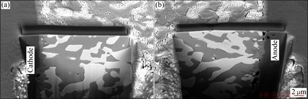
Fig. 4 Cross-sectional FIB-BSE images of position G marked at cathode interface (a) and position H marked at anode interface (b) of line-type interconnect shown in Fig. 2(g)
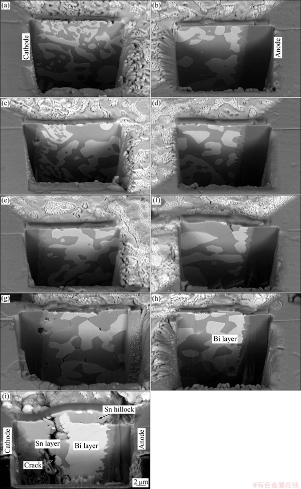
Fig. 5 Cross-sectional FIB-BSE images at different positions of D to L marked in Fig. 3(e) for right-angle type interconnect undergoing current stressing for 288 h (a)-(i) corresponding to positions D-L, respectively
3.2 Mechanism for microregional electrical resistance induced local electromigration damage
Under the current stressing, the mass (or atomic) flux Jem can be expressed as [3]
 (1)
(1)
where Z* is the effective charge number; e is the electron
charge; �� is the resistivity; j is the current density; C is the concentration of the diffusion atom; D is the diffusivity; k is the Boltzmann��s constant; T is the thermodynamic temperature; v is the drift velocity; F is the electromigration force.
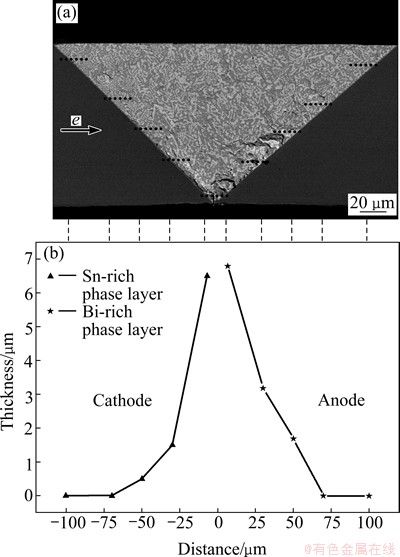
Fig. 6 Illustration of cross-sectional position of right-angle interconnect after current stressing for 288 h (a) and change of thickness of Sn-rich and Bi-rich phase layers at corresponding position along both cathode and anode interfaces (b)
As it is mentioned above, Bi is the main diffusing species in the Cu/Sn-58Bi/Cu interconnect system, therefore, Eq. (1) can also be expressed by
 (2)
(2)
where  is the effective charge number of Bi atom; ��solder is the resistivity of the solder.
In this study, all parameters in Eq. (2) have the same values in both types of solder interconnects. This means that both types of the interconnects should exhibit the same electromigration behavior. However, the experimental results show that the electromigration characteristics, typically the hillocks and cracks, are distinct at different microregions of the right-angle type interconnect, indicating that values of the mass flux Jem at different microregions are also distinct. Thus, it is necessary to further study the distributions of current density (j) at different microregions across the whole section of the right-angle type solder interconnect. As illustrated in Fig. 7, assuming that the electrical resistance of the microregion with a width ��w and a height ��h as well as a length of L (i.e., between the two dashed lines in Fig. 7) consists of two contributions, one is from the solder part and another is from copper. Obviously, due to the geometrical change of the right-angle type solder interconnect and the resistivity difference between the solder and copper, the electrical resistance values in different microregions of the solder interconnect are distinct.
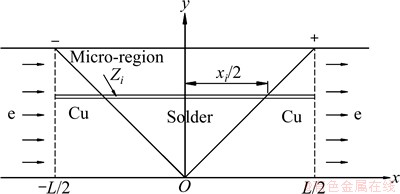
Fig. 7 Schematic illustration of calculation of electrical resistance in microregion in right-angle solder interconnect
Furthermore, assuming that the applied voltage U between the two dashed lines is constant, in this case, the applied voltage in any microregion Zi is constant regardless of the value of xi. Also considering that the distribution of the current density j in any microregion is identical (i.e., j is a constant). Thus, in the microregion Zi, according to the Ohm law and the relation between ji and Ii (i.e., Ji=Ii/��Si), the current density ji can be expressed as
 (3)
(3)
where Ii is the current; Ri is the electrical resistance; L is the total length of the microregion Zi; xi is the length of the solder part in the microregion Zi; ��Cu is the resistivity of copper; ��solder is the resistivity of the solder; ��Si is the cross-sectional area of the microregion Zi in Fig. 7, which is equal to the product of ��w and ��h and is identical in any microregion.
Substituting Eq. (3) into Eq. (2) then yields the mass flux Jem,i in the microregion Zi as follows:
 (4)
(4)
Consequently, the current density in the top side microregion (i.e., xi=L) and the bottom microregion (i.e., xi=0) can be rewritten as follows.
At the top side:
 (5)
(5)
At the bottom corner:
 (6)
(6)
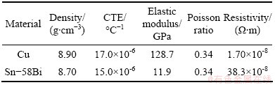
Substituting ��Cu=1.70 �̦���cm and ��Cu=38.3 �̦���cm [23] into Eqs. (5) and (6), then the ratio of the current density between the bottom corner and top side microregions is calculated to be 22.5, that is, jbottom:jtop= ��solder:��Cu=38.3:1.70=22.5:1. Clearly, jbottom is one order of magnitude larger than jtop. Correspondingly, the atomic flux Jem at the bottom corner of the solder interconnect is one order of magnitude greater than that at the top side. This means that the current crowding easily occurs at the microregion with a smaller electrical resistance in any asymmetric solder interconnect.
Based on the above experimental observation and theoretical analysis, it is clear that the asymmetric geometric configuration of solder interconnects can bring about a big difference of electrical resistance in different microregions of an asymmetric interconnect. The current crowding may occur more easily at the microregion with a smaller electrical resistance and consequently lead to severe electromigration damage. In order to further understand the current crowding effect and electromigration behavior in the right-angle type solder interconnect, three dimensional (3D) finite element analysis based on ANSYS 11.0 was performed to simulate the current density distribution, in which the element type SOLID 69 was used. The material properties are given in Table 1. Considering that the IMC layers at both interfaces of the solder interconnect are very thin and the Joule heating can be dissipated timely, the influence of the IMC layers on the current density distribution can be ignored. The finite element model and simulation results are shown in Fig. 8, where an average current density of 1.5��104 A/cm2 is obtained by applying a voltage of 57 V to both ends of the model. Clearly, the maximum value of current density value appears at the bottom corner of the solder interconnect, which is 2.51��104 A/cm2, being 39 times as much as that at the top side with a value of 6.48��102 A/cm2. The simulation results are in good coincidence with the experimental findings and the theoretical analysis.
Table 1 Material properties of Cu and Sn-58Bi solder [23-25]
In this study, all the experimental conditions were kept the same for both types of solder interconnects except the geometrical shape. Thus, it is clear that the current crowding and severe electromigration-induced damage at the bottom corner of the right-angle type solder interconnect are directly related to the inhomogeneous electrical resistance distribution in different microregions of the solder interconnect with asymmetric geometric shape along the direction of electron flow. The smaller electrical resistance in the bottom corner of the interconnect leads to the local current crowding there. Similarly, the electromigration damage in any solder interconnect with an asymmetric shape relative to the electron flow direction can also be explained from the viewpoint of the difference in the microregional electrical resistance. For example, for the paths of electron flow in a flip chip solder joint as illustrated in Fig. 9, the length of ��Path I�� between the entrance and exit is the shortest and the electrical resistance along this path is the smallest. Therefore, the current crowding may occur easily along ��Path I��, leading to voids or cracks near the entrance and hillocks or whiskers near the exit of the electron flow, as indicated by other studies [4,26,27]. In order to get a uniform current density, the thick Cu column bump has been used in the flip chip technology. The results show that the current crowding effect can be alleviated and the electromigration mean life-time of solder joints can be greatly prolonged [7,9].
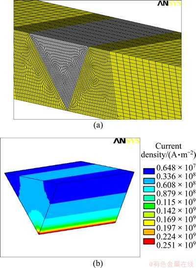
Fig. 8 3D finite element model (a) and simulation results of current density distribution (b) in right-angle type solder interconnect
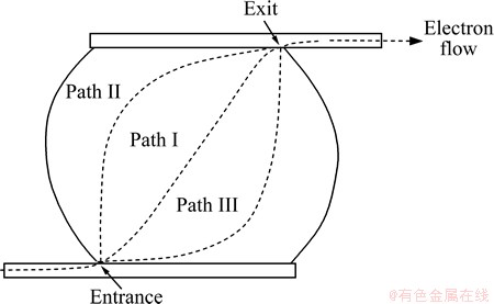
Fig. 9 Schematic of different paths of electron flow in a flip chip solder joint
The surface microstructure evolution shows clearly that the asymmetric shape of the solder interconnect easily results in the localized current crowding and electromigration-induced damage during current stressing, and consequently there are more cracks and hillocks in the right-angle type solder interconnect than in the line-type one. The significant change of the internal morphology near the bottom corner of the right-angle type interconnect is due to the severe segregation of Sn-rich phase and Bi-rich phase, which is much severer than that on the surface. The analytical correlation between the current density and the electrical resistance in a microregion of the asymmetric solder interconnect shows that the small local electrical resistance along the path of electron flow is the key factor leading to the current crowding and severe electromigration-induced damage. Therefore, it is suggested not to employ the solder interconnect with an asymmetric shape along the electron flow path in electronic package structures.
4 Conclusions
1) The electromigration-induced local degradation of microstructures, in terms of segregation of Bi-rich phase and formation of microcracks, in the asymmetric solder interconnect is much severer than that in the symmetrical one, due to the strong current crowding effect in the former.
2) The heterogeneity of microregional resistance in the asymmetric solder interconnect is the key factor leading to the current crowding of the local region with small electrical resistance and the resultant electromigration damage, and an analytical method is proposed to quantitatively evaluate the current crowding effect.
3) In the right-angle type solder interconnect, the electromigration damage easily occurs near the bottom corner position owing to the smallest local resistance and severest current crowding effect. The change of thickness of Bi-rich and Sn-rich phase layers along the whole cathode and anode interfaces is non-linear.
References
[1] ZENG K, TU K N. Six cases of reliability study of Pb-free solder joints in electronic packing technology [J]. Materials Science and Engineering R, 2002, 38(2): 55-105.
[2] TU K N. Recent advances on electromigration in very-large-scale-integration of interconnects [J]. Journal of Applied Physics, 2003, 94(9): 5451-5473.
[3] CHAN Y C, YANG D. Failure mechanisms of solder interconnects under current stressing in advanced electronic packages [J]. Progress in Materials Science, 2010, 55(5): 428-475.
[4] YEH E C C, CHOI W J, TU K N, ELENIUS P, BALKAN H. Current-crowding-induced electromigration failure in flip chip solder joints [J]. Applied Physics Letters, 2002, 80(4): 580-582.
[5] ZHANG L Y, OU S Q, HUANG J, TU K N, GEE S, NGUYEN L. Effect of current crowding on void propagation at the interface between intermetallic compound and solder in flip chip solder joints [J]. Applied Physics Letters, 2006, 88(1): 012106.
[6] LU Y D, HE X Q, EN Y F, WANG X, ZHUANG Z Q. Polarity effect of electromigration on intermetallic compound formation in SnPb solder joints [J]. Acta Materialia, 2009, 57(8): 2560-2566.
[7] XU L H, HAN J K, LIANG J J, TU K N, LAI Y S. Electromigration induced high fraction of compound formation in SnAgCu flip chip solder joints with copper column [J]. Applied Physics Letters, 2008, 92(26): 262104.
[8] HUANG Ming-liang, CHEN Lei-da, ZHOU Shao-ming. Effect of electromigration on interfacial reaction in Ni/Sn3.0Ag0.5Cu/Cu flip chip solder joints [J]. Acta Metallurgica Sinica, 2012, 48(3): 321-328. (in Chinese)
[9] HAN J K, CHOU D, FUJIYOSHI M, CHIWATA N, TU K N. Current density redistribution from no current crowding to current crowding in Pb-free solder joints with an extremely thick Cu layer [J]. Acta Materialia, 2012, 60(1): 102-111.
[10] LEE T Y, TU K N, FREAR D R. Electromigration of eutectic SnPb and SnAg3.8Cu0.7 flip chip solder bumps and under-bump metallization [J]. Journal of Applied Physics, 2001, 90(9): 4502-4508.
[11] DING M, WANG G T, CHAO B, HO P S, SU P, UEHLING T. Effect of contact metallization on electromigration reliability of Pb-free solder joints [J]. Journal of Applied Physics, 2006, 99(9): 094906.
[12] NAH J W, SUH J O, TU K N, YOON S W, RAO V S, KRIPESH V. Electromigration in flip chip solder joints having a thick Cu column bump and a shallow solder interconnect [J]. Journal of Applied Physics, 2006, 100(12): 123513.
[13] KSUALKE P, SCHMIDT W, TITERLE L, BOHNAKER H, OPPERT T, ZAKEL E. Solder ball bumper SB2��A flexible manufacturing tool for 3-dimensional sensor and microsystem packages [C]// Proceedings of IEMT Symposium. Berlin, Germany: IEEE, 1998: 70-75.
[14] YUE W, ZHOU M B, QIN H B, LI X P, MA X, ZHANG X P. A comparative investigation of the electromigration behavior between wedge-type and line-type Cu/Sn3.0Ag0.5Cu/Cu interconnects [C]// IEEE 12th International Conference on Electronic Packaging Technology & High Density Packaging. Shanghai: IEEE, 2011: 971-975.
[15] YUE Wu, QIN Hong-bo, ZHOU Min-bo, MA Xiao, ZHANG Xing-ping. Influence of solder joint configuration on electromigration behavior and microstructural evolution of Cu/Sn-58Bi/Cu microscale joints [J]. Acta Metallurgica Sinica, 2012, 48(6): 678-686. (in Chinese)
[16] CHEN C M, HUANG C C, LIAO C N, LIOU K M. Effects of copper doping on microstructural evolution in eutectic SnBi solder strips under annealing and current stressing [J]. Journal of Electronic Materials, 2007, 36(7): 760-765.
[17] GU X, CHAN Y C. Electromigration in line-type Cu/Sn-Bi/Cu solder joints [J]. Journal of Electronic Materials, 2008, 37(11): 1721-1726.
[18] LIU C Y, CHEN C, TU K N. Electromigration in Sn-Pb solder strips as a function of alloy composition [J]. Journal of Applied Physcis, 2000, 88(10): 5703-5709.
[19] YANG Q L, SHANG J K. Interfacial segregation of Bi during current stressing of Sn�CBi/Cu solder interconnect [J]. Journal of Electronic Materials, 2005, 34(11): 1363-1367.
[20] WU A T, GUSAK A M, TU K N, KAO C R. Electromigration-induced grain rotation in anisotropic conducting beta tin [J]. Applied Physcis Letters, 2005, 86(24): 241902.
[21] WU A T, HSIEH Y C. Direct observation and kinetic analysis of grain rotation in anisotropic tin under electromigration [J]. Applied Physcis Letters, 2008, 92(12): 121921.
[22] LU M H, SHIH D Y, LAURO P, GOLDSMITH C, HENDERSON D W. Effect of Sn grain orientation on electromigration degradation mechanism in high Sn-based Pb-free solders [J]. Applied Physics Letters, 2008, 92(21): 211909.
[23] SUN J, XU G C, GUO F, XIA Z D, LEI Y P, SHI Y W, LI X Y, WANG X T. Effects of electromigration on resistance changes in eutectic SnBi solder joints [J]. Journal of Materials Science, 2011, 46(10): 3544-3549.
[24] YOSHIDA K, MORIGAMI H. Thermal properties of diamond/copper composite material [J]. Microelectronic Reliability, 2004, 44(2): 303-308.
[25] HARPER J M E, CABRAL C Jr, ANDRICACOS P C, GIGNAC L, NOYAN I C, RODBELL K P, HU C K. Mechanisms for microstructure evolution in electroplated copper thin films near room temperature [J]. Journal Applied Physics, 1999, 86(5): 2516-2525.
[26] YIN Y H, HU Y C, TAI C M, KAO C R, TU K N. In situ observation of the void formation and propagation mechanism in solder joints under current stressing [J]. Acta Materialia, 2005, 53(7): 2029-2035.
[27] OUYANG F Y, CHEN K, TU K N, LAI Y S. Effect of current crowding on whisker growth at the anode in flip chip solder joints [J]. Applied Physics Letters, 2007, 91(23): 231919.
�� �䣬�غ첨������������ �磬����ƽ
����������ѧ ���Ͽ�ѧ�빤��ѧԺ������ 510640
ժ Ҫ������ԭλSEM�۲졢FIB������������Ԫ(FE)ģ���о��˷ǶԳƽṹCu/Sn-58Bi/Cu �����е�Ǩ���������֯�ݱ估�����ˡ�����������ǶԳƽṹ�����и�Bi��ƫ�ۺ����Ƶȵ�Ǩ������Զ�ȶԳƺ��������أ�FIB-SEM�۷��������ʾ�ǶԳƺ������ص��������ϸ������ڵ�������ǵ��º�������ϵ����Ǿ��ȷֲ������ص�Ǩ������Ĺؼ����أ����۷�����ģ��������������ӵ���������ں������������С��λ�á�
�ؼ��ʣ������裻�ǶԳƺ��㣻��Ǩ��Σ��������ӵ������״ЧӦ
(Edited by Hua YANG)
Foundation item: Project (51275178) supported by the National Natural Science Foundation of China; Project (20110172110003) supported by Research Fund for the Program of Higher Education of China
Corresponding author: Xin-ping ZHANG; Tel: +86-20-22236396; Fax: +86-20-22236393; E-mail: mexzhang@scut.edu.cn
DOI: 10.1016/S1003-6326(14)63233-7

