
Sub-micron-structure machining on silicon by femtosecond laser
Hung-Yin TSAI 1, Shao-Wei LUO1, Chih-Wei WU 2, Shing-Hoa WANG 2
1. Department of Power Mechanical Engineering, National Tsing Hua University, Hsinchu, Taiwan, China;
2. Department of Mechanical and Mechatronic Engineering, National Taiwan Ocean University,
Keelung, Taiwan, China
Received 2 March 2009; accepted 30 May 2009
Abstract: Sub-micron-structure machining on silicon substrate was studied by direct writing system of femtosecond laser with the central wavelength of 800 nm, pulse duration of 120 fs and repetition rate of 1 kHz. Three kinds of experiments were conducted: 1) the effect of photoresist on silicon; 2) machinability of different orientations of silicon; and 3) the size of micro-structure and the cross-section shape. Photoresist SU8 was coated onto silicon substrates in thicknesses of 100 ��m. SU8 remained on the silicon substrate while the silicon under the machined SU8 was removed after laser machining. Orientations of (100), (110), and (111) silicon substrates were machined with the laser power of 60 ��W and the scanning speed of 3 mm/min. Spike morphologies were observed on all three orientations of silicon substrates without obvious directional difference of these spikes on different silicon substrates. In addition, the ablation threshold energies were also similar. In the consideration of ablation energy, one numerical model of the machining parameters has been proposed to simulate the cross-section of the micro-structure. The predicted shape by simulation can fit the profile of the cross-section shape well.
Key words: femtosecond laser; SU8; silicon; sub-micron structure
1 Introduction
Due to the versatile applications of optical components, the optical characteristics of micro-structure need to be improved and applied at the wide wavelength band. Regular array structures or periodical patterns can satisfy the requirement of the advanced optical applications. It is very important to develop the manufacturing technology for the optical component of certain pattern used at different wavelengths.
The machining mechanism of femtosecond laser was firstly proposed by NORRIS in 1990[1]. He proposed that the laser ablation occurred after multiple-photon absorption to break the chemical bond in material. The mechanism is different from thermal melting or vaporization by conventional laser.
Femtosecond laser is characterized by: 1) cold or heatless machining mechanism, 2) high resolution that beats diffraction limit, 3) clean machined surface and high efficiency, 4) any materials, and 5) machining/ ablating on the focal spot. Compared with the traditional laser, femtosecond laser can fabricate nanostructures or complicated three-dimension micro-structures.
According to the above characteristics of femtoseond laser, this innovative machining method can be applied to many fields, including photonic crystal fabrication by two-photon absorption(TPA)[2], array structures by one laser pulse lithography with micro array lenses[3], sub-30 nm structure machined by femto- second laser with near field system[4-5], and grating structures by laser interference[6-7].
For the numerical modeling, JIANG and TSAI [8-13] proposed the Gaussian formula to express the laser intensity, which was combined with the heat-transfer process and the free-electron distribution in bulk material, from 1993 to 1996. With the numerical modeling, the equations can be used to calculate the ablation shape by a laser pulse correctly.
2 Experimental
Direct writing system of femtosecond laser with the central wavelength of 800 nm, pulse duration of 120 fs, repetition rate of 1 kHz, and 10�� object lens with NA 0.3 is used in the current study. The schematic diagram is shown in Fig.1. Photoresist of SU8 is coated onto (110) substrates in thickness of 100 ��m. Silicon substrates with (100), (110), and (111) orientations were machined. The passing of laser beam was switched by a mechanical shutter and different laser powers were adjusted to ablate the samples on a motion stage. The laser writing route is shown in Fig.2. The machined surface is observed by scanning electron microscopy(SEM).
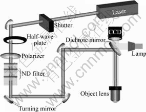
Fig.1 Schematic diagram of experimental setup
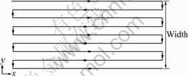
Fig.2 Sketch map of scanning route
3 Experimental results
3.1 SU8
Fig.3(a) shows the SEM image of SU8 machined by using the laser power of 60 ��W and the scanning speed of 3 mm/min. It shows no obvious ablation in the central part of machined area except the edges where the laser beam moves slowly. Fig.3(b) shows the SEM image of the silicon substrate under SU8, which is removed after femtosecond laser machining. Since the NA number of the object lens is not large enough, the focal spot size is not small enough. Once the laser fluence is below the ablated threshold of SU8 as this case, the laser beam passes through the SU8 to machine the silicon substrate, and therefore the ablation occurs.
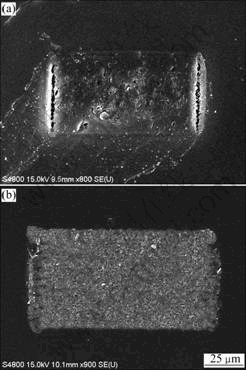
Fig.3 SEM images of SU8 (a) and substrate (b) at laser power of 60 ��W and scanning speed of 3 mm/min
Even the laser power is increased to 100 ��W with the scanning speed of 3 mm/min, the similar machined results are shown in Fig.4. The SU8 phtotoresist on the silicon substrate could be ablated as a rectangle structure when the laser power is increased to over 200 ��W. Fig.5 shows the ablated photoresist structures on Si(110) substrates with laser power of 200 ��W, 600 ��W, and 1 mW, respectively. All SU8 coated substrates were etched by acetone to remove the SU8 photoresist off before taking SEM image.
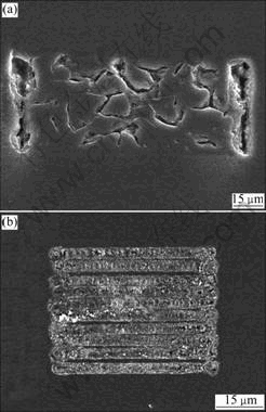
Fig.4 SEM images of SU8(a) and substrate(b) at laser power of 100 ��W and scanning speed of 3 mm/min
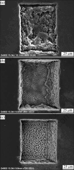
Fig.5 SEM images of substrates under SU8 at scanning speed of 3 mm/min and laser power of 200 ��W(a), 600 ��W(b), and 1 mW(c)
3.2 Silicon substrates with (100), (110), and (111) orientations
These experiments were proceeded at different scanning speeds with identical laser power of 60 ��W. Fig.6(a) shows the result of the line-machining on Si(111) with the scanning speed of 1 mm/min. The depth of an area between two continuous holes by laser pulse is close to the depth. Fig.6(b) shows the result on Si(111) with the scanning speed of 3 mm/min. The two continuous holes are slightly connected by a shallow trench resulted from affected zone of single laser pulse. Fig.6(c) shows the result on Si(111) with the scanning speed of 5 mm/min. The separated holes can be easily observed and there is nearly no interacted zone between two ablated holes.
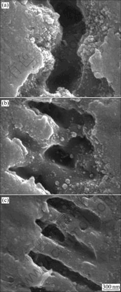
Fig.6 Line machining on Si(111) by laser power of 60 ��W and scanning speed of 1 mm/min(a), 3 mm/min(b) and 5 mm/min (c)
From the previous experimental results, the scanning speed of 3 mm/min is chosen for laser machining on different orientations of silicon wafers. Figs.7(a)-(c) show the machining results of silicon substrates with (100), (110), (111) orientations by 60 ��W laser power and 3 mm/min scanning speed. There is no obvious difference of ablated threshold energy between these three kinds of silicons, though the morphologies at the bottoms seem not similar.
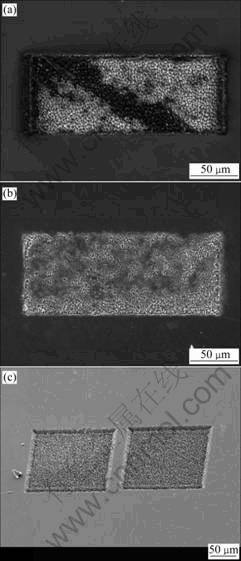
Fig.7 SEM images of rectangle structure machining on Si (111) (a), (100) (b), (110) (c) at laser power of 60 ��W and scanning speed of 3 mm/min
Compared with the machined silicon substrate with (110) orientation in Figs.5(a)-(c), the spike morphology at the bottom can be obtained using the higher laser power than the threshold energy, and the whole rectangular shape shows clearer edge.
3.3 Single hole structure
Fig.8 shows the smallest hole structure with diameter of 400 nm obtained in the current study by a laser pulse of 60 ��W, which is close to the ablated threshold.
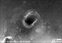
Fig.8 SEM image of smallest hole-structure with diameter of 400 nm by laser pulse with power of 60 ��W
4 Numerical modeling
The process of photo-ionization by femtosecond laser can be divided into two parts: one is direct photoionization after electron absorbing enough photon energy; the other is impact ionization. When the kinetic energy of a free electron becomes sufficiently high by absorbing photons, part of the energy may transfer to a bound electron by collisions to overcome the ionization potential and produce two free electrons. The function of free electron distribution can be calculated by[10]
 (1)
(1)
where ne(t, r, z) is the free electron density; ��(I) is the
impact ionization term; P(I) is the photoionization term; t is the time; r is the distance to the Gaussian beam axis; z is the depth from the surface of the bulk material; I is the laser intensity inside the bulk material which is a function of t, r, and z.
Assume that the impact ionization is linearly proportional to the laser intensity as follows[14]:
��(I)=aiI(t, r, z) (2)
where ai is a constant, which is 5.88 cm2/J for silicon. The photoionization rate can be expressed as a function of laser intensity by[10]
P(I)=��N[I(t, r, z)]N (3)
where ��N is the cross-section of N-photon absorption. For fused silica (bandgap: 9 eV) and the laser wavelength of 800 nm used in the present study, one photon is required to free a bound electron and, hence, ��N=1.6��1018 cm-3?ps-1(cm2/TW)[15-16]��and the absorption number N=1.
The original laser beam before it interacts with the material is assumed to be a Gaussian distribution in time and space. The laser intensity can be described by[10]
I(t, r, z)=I0[1-R(t, r)]?
 (4)
(4)
where R(t, r) is the reflectivity of material, for silicon it is 0.328 at wavelength of 800 nm; r0 is the radius of the laser beam, 1.45 ��m; tp is the pulse duration, 120 fs; ��(t, r, z) is the absorption coefficient of the material, for silicon it is 7.8��102 cm-1[17].
And I0 is the peak intensity given by[18]
 (5)
(5)
where F is the fluence, 1.8 J/cm in this study.
As for ablation depth calculation, it is assumed that the actual fluence at the ablation depth, d, equals absorbed threshold fluence, F(z=d)=(1-r)Ft. Based on this assumption, the ablation depth can be estimated by [8]:
 (6)
(6)
where Ft is the threshold fluence. It is widely assumed that ablation starts when the free electron density reaches the critical density. According to this assumption, threshold fluence can be considered as the minimal fluence to create the critical density. Based on this assumption, the theoretical threshold logarithmically depends on the value of critical density [14]:
 (7)
(7)
where nc is the critical density, which relates to laser central wavelength and the permittivity of bulk material, given by[18]:
 (8)
(8)
where me is the electron mass, 9.109 381 88��10-31 kg; c is the speed of light, 3��108 m/s; e is the electron charge, and �� is the laser wavelength of 800 nm. n0 is the seed electrons generated by multiphoton ionization. The free electron distribution and ablation curve can be determined from the relationship between n0 and threshold.
Fig.9 shows the distribution of free electrons by laser pulse in bulk material. The ablated depth can be decided from the position of broken line as shown in Fig.10. The broken line is determined from the intersec- tion point of fluence and n0 curve. According to the depth, the ablation shape can be drawn from the distribution of free electrons, as shown in Fig.9.
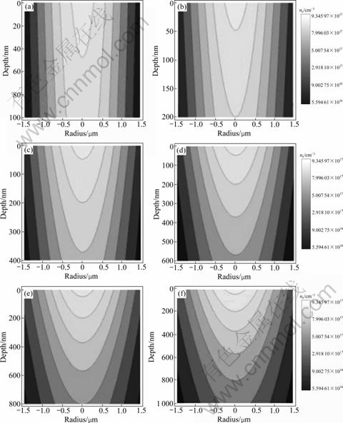
Fig.9 Free electrons distribution in silicon by one pulse at power of 60 ��W: (a) 100 nm; (b) 200 nm; (c) 400 nm; (d) 600 nm; (e) 800 nm; (f) 1 000 nm
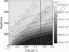
Fig.10 Depth of free electrons distribution as function of laser fluence
Fig.11(a) shows the result from the numerical modeling and Fig.11(b) shows the AFM image of the cross section of the practical ablation profile in Fig.6(b). The broken lines in Fig.11(a) and Fig.11(b) are the same profile of the approximate curve to the cross section. The simulation results agree well with the experimental ones.
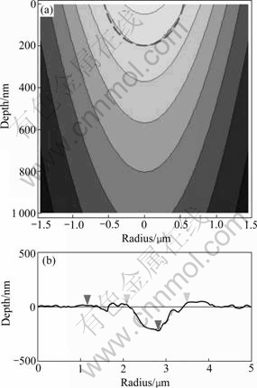
Fig.11 Electrons distribution in Fig.9 at depth of 200 nm (a) and fitted AFM profile image (b)
5 Conclusions
The machinability on different characteristics of silicon substrates has been studied and one numerical model has been proposed to predict the cross-section shape by femtosecond laser. For the case of photoresist SU8 coated onto silicon substrates, SU8 remained on the silicon substrate while the silicon under the machined photoresist was removed after laser machining since the focal spot size is not small enough. Orientations of (100), (110), and (111) silicon substrates were machined with the laser power of 60 ��W and the scanning speed of 3 mm/min. Spike morphologies were observed on all three orientations of silicon substrates without obvious directional difference of these spikes on different silicon substrates. The smallest hole obtained by femtosecond laser has the diameter of about 400 nm at the laser pulse of 60 ?W. In the consideration of ablation energy, one numerical model of the machining parameters has been proposed to simulate the cross-section of the micro-structure. The predicted shape by simulation can fit the profile of the cross-section shape well. So femtosecond laser has the micro/ nano-fabrication potential to pattern different structures in the optical applications as CNC machining to mechanical industries. In micro/nano-structure application, femtosecond laser machining will play a very important role in the coming future.
Acknowledgments
The authors gratefully acknowledge Prof. Hai-Lung TSAI (Mechanical Engineering, Missouri University of Science and Technology, USA) for his laser system and the National Science Council for supporting the research project under the contract No. NSC�C97�C2622�CE�C007�C 004-CC3.
References
[1] MYAING M T, URAYAMA J, NORRIS T B, BRAUN A. Nonlinear propagation of negatively chirped pulses: Maximizing the peak intensity at the output of a fiber probe [J]. Opt Express, 2000, 7: 210-214.
[2] SEET K K, MIZEIKIS V, JUODKAZIS S, MISAWA H. Three-dimensional circular spiral potonic crystal structures recordedby femtosecond pulses [J]. J Non-Cryst Solids, 2006, 352: 2390-2394.
[3] MATSUO S, MIYAMOTO T, TOMITA T. Laser microfabrication of photoresist rod array using a microlens array [C]// Proceeding of Lasers and Electro-Optics, 2005. CLEO/Pacific Rim 2005. 2005: 1731-1733.
[4] LIN Y, HONG M H, WANG W J, LAW Y Z, CHONG T C. Sub-30 nm lithography with near-field scanning optical microscope combined with femtosecond laser [J]. Appl Phys A, 2005, 80: 461-465.
[5] LIN Y, HONG M H, WANG W J, WANG Z B, CHEN G X, XIE Q, TAN L S, CHONG T C. Surface nanostructuring by femtosecond laser irradiation through near-field scanning optical microscopy [J]. Sens Actuators A, 2007, 133: 311-316.
[6] VENKATAKRISHNAN K, SIVAKUMAR N R, HEE C W, TAN B, LIANG W L, GAN G K. Direct fabrication of surface-relief grating by interferometric technique using femtosecond laser [J]. Appl Phys A, 2003, 77: 959-963.
[7] TAN B, SIVAKUMAR N R, VENKATAKRISHNAN K. Direct grating writing using femtosecond laser interference fringes formed at the focal point [J]. J Opt A: Pure Appl Opt, 2005, 7: 169-174.
[8] JIANG L, TSAI H L. Femtosecond laser ablation: Challenges and opportunities [C]// Proceeding of NSF Workshop on Research Needs in Thermal, Aspects of Material Removal, Stillwater, OK, 2003: 163-177.
[9] JIANG L, TSAI H L. Prediction of crater shape in femtosecond laser ablation of dielectrics [J]. Journal of Phys D: Appl Phys, 2004, 37(B): 1492-1496.
[10] JIANG L, TSAI H L. Energy transport and material removal in wide bandgap materials by a femtosecond laser pulse [J]. Int J Heat Mass Transfer, 2005, 48: 487-499.
[11] JIANG L, TSAI H L. Repeatable nanostructures in dielectrics by femtosecond laser pulse trains [J]. Appl Phys Lett, 2005, 87: 151104.
[12] JIANG L, TSAI H L. Improved two-temperature model and its application in ultrashort laser heating of metal films [J]. J Heat Transfer, 2005, 127: 1167-1173.
[13] JIANG L, TSAI H L. Plasma modeling for ultrashort pulse laser ablation of dielectrics [J]. J Appl Phys, 2006, 100: 023116.
[14] STUART B C, FEIT M D, HERMAN S, RUBENCHIK A M, SHORE B W, PERRY M D. Nanosecond-to-femtosecond laser-induced breakdown in dielectrics [J]. Phys Rev B, 1996-II, 53: 1749-1761.
[15] MA W, WUA Y, HAN J, GU D, GAN F. Large three-photon absorption cross-section in a novel class of bis-(N-carbazolyl) fluorene derivatives [J]. Chem Phys Lett, 2005, 403: 405-409.
[16] BRISTOW A D, ROTENBERG N, DRIEL H M V. Two-photon absorption and Kerr coefficients of silicon for 850-2200 nm [J]. Appl Phys Lett, 2007, 90: 191104.
[17] ASPNES D E, STUDNA A A. Dielectric functions and optical parameters of Si, Ge, GaP, GaAs, GaSb, InP, InAs, and InSb from 1.5 to 6.0 eV [J]. Phys Rev B, 1983, 27: 985-1009.
[18] STUART B C, FEIT M D, RUBENCHIK A M, SHORE B W, PERRY M D. Laser-induced damage in dielectrics with nanosecond to sub-picosecond pulses [J]. Phys Rev Lett, 1995, 74: 2248-2251.
Corresponding author: Hung-Yin TSAI; Tel: +886-3-5742343; E-mail: hytsai@pme.nthu.edu.tw
(Edited by YANG Bing)