文章编号:1004-0609(2014)11-2827-09
可见光响应型Cu-Ti-O纳米管阵列的阳极氧化制备及表征
马 清1,陈建军1,刘绍军2,檀满林1,符冬菊1,程立金2
(1. 深圳清华大学研究院 低碳能源与节能技术重点实验室,深圳 518057;
2. 中南大学 粉末冶金国家重点实验室,长沙 410083)
摘 要:通过阳极氧化在Cu30Ti70合金基体上制备出高度有序的Cu掺杂Cu-Ti-O纳米管阵列,并讨论了阳极氧化时间对Cu-Ti-O纳米管阵列形貌和结构影响。结果表明:在O2气氛中450℃退火晶化2 h后,Cu-Ti-O纳米管阵列在400~650 nm波长范围内表现出较强的可见光响应性能,其本征吸收带边和可见光吸收带边最大值分别红移至470 nm和760 nm;Cu掺杂后形成的氧空位促进了Cu-Ti-O纳米管锐钛矿向金红石相的转变;随着阳极氧化时间的延长,Cu-Ti-O纳米管阵列长度增加,管壁厚度减薄,且在O2气氛中450 ℃退火2 h后,金红石相转变量增加。
关键词:Cu-Ti-O纳米管;Cu-Ti合金;阳极氧化;可见光响应
中图分类号:TQ153.6;O643 文献标志码:A
Preparation and characterization of visible-light-sensitive anodic Cu-Ti-O nanotube arrays
MA Qing1, CHEN Jian-jun1, LIU Shao-jun2, TAN Man-lin1, FU Dong-ju1, CHENG Li-jin2
(1. Key Laboratory of Low-carbon Energy and Energy-saving Technology,
Research Institute of Tsinghua University in Shenzhen, Shenzhen 518057, China;
2. State Key Laboratory of Powder Metallurgy, Central South University, Changsha 410083, China)
Abstract: Well organized Cu-Ti-O nanotube arrays with enhanced visible light response were prepared on Cu30Ti70 alloy substrate by anodization. The influences of anodization time on the morphology, crystalline structure and photocatalytic activity of Cu-Ti-O nanotube arrays were further investigated. The results show that the stronger visible-light-sensitive care observed at the wavelength of 400-650 nm, the intrinsic and visible light absorption edge are red shift to about 470 nm and 760 nm, respectively. The oxygen vacancies induced by the high concentration Cu dopant into the Cu-Ti-O nanotube play a favorable role in determining anatase to rutile phase transformation. With prolonging anodization time,the Cu-Ti-O nanotube length increases while the wall thickness decreases as well as rutile phase transformation increasing after crystallization in O2 annealing at 450 ℃ for 2 h.
Key words: Cu-Ti-O nanotube; Cu-Ti alloy; anodization; visible-light-sensitive
二氧化钛(TiO2)纳米管以其优异的物理和化学性能在染料敏化太阳电池和光催化领域得到了广泛应用。然而,TiO2的禁带宽度为3.0~3.2 eV,使得只有小于5%的紫外光区域的太阳光能够被吸收利用,因此,严重制约了其对太阳光的高效吸收。为了改善TiO2的可见光响应性能,各国研究者对此展开了广泛而深入的研究,其中最为行之有效的方法是通过掺杂来改变其电子和能带结构[1],如过渡金属[2-3]和非金属[4-5]元素以及多元共掺杂[6]等。在众多的过渡金属元素中,Cu与Ti元素原子半径相近且储量丰富、成本低以及无毒,被认为是比较适合的掺杂元素之一[7]。此外,作为p型半导体,氧化铜(CuO)和氧化亚铜(Cu2O)带隙更窄,分别为1.2~1.5 eV和2.0~2.2 eV,因此,Cu掺杂纳米晶TiO2薄膜材料作为光电极能够表现出优异的光电化学性能[8]。
TiO2纳米管的制备方法通常有溶胶-凝胶法[9]、水热法[10]、模板法[11]和电化学阳极氧化法[12]等。采用化学方法制备TiO2纳米管时,工艺复杂、可控程度低、且制备出的TiO2纳米管有序度较低。贾春阳等[13]通过溶胶-凝胶法和水热法制备出管长约为300 nm、管径约为10 nm的Cu掺杂TiO2纳米管,但其纳米管结构易遭到破坏、纳米管有序度低、易团聚且工艺复杂。电化学阳极氧化以其工艺简单、成本低廉、可控程度高以及可重复性好等优点,引起了各国研究者的高度关注。然而,目前鲜有直接在Cu-Ti合金基体上通过阳极氧化制备Cu-Ti-O纳米管阵列的相关报道。
也有研究者首先在FTO基体上磁控溅射出Cu-Ti[14]与Fe-Ti[15]合金薄膜,然后电化学阳极氧化生长出掺杂改性的Cu-Ti-O与Fe-Ti-O纳米管阵列,但此方法设备昂贵且工艺复杂、薄膜质量难以保证。也有研究者通过阳极氧化直接在Ti-Zr[16]、TiTa[17]、TiZrNb[18]和TiNbTaZr[19]等合金片状基体上制备出一维纳米结构的掺杂TiO2纳米管阵列,然而,相关报道鲜有对其光电化学性能进行深入表征研究。
本文作者在深入讨论Cu-Ti合金基体上Cu-Ti-O纳米管阵列生长机理的基础之上[20],进一步讨论了阳极氧化时间对Cu-Ti-O纳米管形貌、结构和性能等的影响。本文作者制备的Cu-Ti-O纳米管阵列具有较强的可见光响应性能,且工艺简单、成本低廉、可控程度高。
1 实验
1.1 纳米管试样制备
实验用Cu30Ti70合金为中南大学粉末冶金国家重点实验室采用电弧熔融法制备。首先通过线切割将合金锭加工成厚度约为1 mm的薄片,然后分别用标号为800、1000和2000的金相砂纸打磨并抛光,最后在丙酮、无水乙醇和蒸馏水中分别超声清洗10 min后烘干备用。电化学阳极氧化实验在室温(25 ℃)下于20 V恒电压下分别反应5、30、60、120和180 min,Cu30Ti70合金片为阳极,高纯Pt片为对电极,电解液组成为0.3 mol/L NH4F+2% H2O+98%甲酰胺(体积分数)。随后,TiO2纳米管阵列前驱体在管式马弗炉中以2 ℃/min的升温速率升温至450 ℃并保温2 h,试样随炉冷却,退火气氛为99.99%高纯氧气。
1.2 试样表征
采用Hitachi-S4700场发射扫描电子显微镜(FESEM)对合金基体与Cu-Ti-O纳米管阵列形貌进行表征。采用Rigaku X-ray diffractometer D/max 2500PC X射线衍射仪(XRD)对TiO2纳米管试样的物相结构进行表征,光源为Cu Kα,工作电压为40 kV,工作电流为200 mA。Cu-Ti-O纳米管阵列的微区结构采用瑞士Renishaw Invia Micro-Raman Spectroscope System激光拉曼光谱仪对纳米晶TiO2的结构和成分进行Raman表征,波长514.5 nm氩激光作为激发光源,累积扫描3次。试样元素组成和化学状态通过美国Thermo ESCALAB250 X射线光电子能谱(X-ray Photoelectron Spectroscope,XPS)进行表征,X射线源为铝的的单色化X射线,能量为1486.6 eV。
2 结果与讨论
2.1 形貌分析
图1所示为阳极氧化反应前后Cu-Ti基体表面形貌的FESEM像。图1(a)为阳极氧化前Cu-Ti基体经抛光后表面形貌的FESEM像,可以看出,在阳极氧化以前,Cu30Ti70基体中存在两个形貌截然不同的区域。为了进一步确任两个区域中的组成,分别对其进行了EDS表征,如图1(a)所示,大面积的灰色区域Cu含量较高,为富Cu相,n(Cu)/n(Ti)=1/2,而点缀其中的花瓣状黑色区域Ti含量较高,为富Ti相,Cu与Ti摩尔比为1.73:98.27。
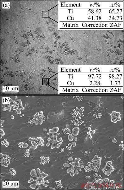
图1 阳极氧化前后Cu30Ti70基体表面形貌FESEM像
Fig. 1 FESEM images of Cu30Ti70 substrate before (a) and after (b) anodization
图1(b)所示为阳极氧化反应后试样表面形貌的放大倍数FESEM像。由图1(b)可以看出,Cu-Ti合金基体在阳极氧化反应之后也存在两个形貌不同的区域,富Cu相由反应前的灰色变成阳极氧化反应之后的黑色区域,而富Ti相经过阳极氧化反应之后则变成了亮灰色的花瓣状。在阳极氧化反应结束后,电解液中出现了许多黑色的悬浮颗粒,这是由于Cu在电解液中的溶解所造成的。相反,在阳极氧化纯Ti基体的过程中则没有观察到此现象的发生。
图2所示为阳极氧化5、30、60、120和180 min后富Cu相和富Ti相上Cu-Ti-O纳米管阵列表面形貌的FESEM像。在阳极氧化5min后,富Cu相表面有较多覆盖物,如图2(a)所示;而在富Ti相上生长的Cu-Ti-O纳米管长度较短且有序度较差,如图2(b)所示;在阳极氧化30 min后,如图2(c)和(d)所示,Cu-Ti-O纳米管阵列有序度增加,富Cu相表面仍残留一部分覆盖物,Cu-Ti-O纳米管有序度较低,且开口端圆形度较差,而富Ti相上Cu-Ti-O纳米管阵列管长约为250~300 nm。
在图2(e)中,富Cu相上生长的Cu-Ti-O纳米管的有序度和开口端圆形度增加,且能够清楚地观察到富Cu相和富Ti相由于两相性质差异而导致的表面形貌的变化; 在图2(f)中,富Ti相上生长的Cu-Ti-O纳米管长度约为500 nm。随着阳极氧化时间的延长,在20V恒压下阳极氧化120 min后,富Cu相上生长的Cu-Ti-O纳米管管径增加,如图2(g)所示;富Ti相上生长的Cu-Ti-O纳米管长度约为600 nm,如图2(h)所示。在20V恒压下阳极氧化180 min后,富Cu相区域生长的Cu-Ti-O纳米管管壁厚度和管径变化不大,如图(i)所示; 在富Ti相上,Cu-Ti-O纳米管长度约为800 nm,管壁厚度继续减薄并出现部分破损,如图(j)中A、B和C点所示。在O2气氛中450 ℃退火晶化2 h后,Cu-Ti-O纳米管阵列维持了非常完好地纳米管结构。
在各种Ti合金基体的阳极氧化制备金属元素掺杂的TiO2纳米管阵列的报道中,同样的现象也发生在Ti-Zr[16]、Ti-Ta[17]、Ti-6Al-4V[21]等合金体系中。这主要是由于与纯Ti基体相比,在很多的Ti合金中都表现出α与β相共存的微观结构[22]。其中,α相为六方密堆积结构(HCP),因此,具有稳定六方密堆积的元素如Al等容易在Ti合金中富集,而诸如V、Mn、Nb、Mo和Ta等具有稳定面心立方结构(BCC)的元素则容易在具有面心立方结构的β相中富集。由于以上元素在电化学阳极氧化钛合金过程中具有不同的化学溶解速率和反应速率,因此,对TiO2纳米管阵列的有序性有重要影响。
2.2 结构分析
图3所示为20V恒压阳极氧化120 min和180 min后生长的Cu-Ti-O纳米管阵列在O2气氛中450 ℃退火晶化2 h后的XRD谱。由图3可以看出,两组试样均在2θ为25.6°和27.8°附近分别出现了锐钛矿相(101)和金红石相(110)晶面特征衍射峰,而以往的研究表 明[23],对于未经掺杂的阳极氧化制备的TiO2纳米管阵列而言,在去除Ti基体由于吞噬效应对TiO2纳米管相转变影响后,高度结晶的锐钛矿相能够保持到800 ℃。由此表明,O2气氛中450 ℃退火晶化2 h后,在XRD谱中出现的金红石相(110)晶面特征衍射峰是由于Cu成功掺杂进入TiO2晶格,并在一定程度上促进了Cu-Ti-O纳米管阵列中锐钛矿向金红石相的转变。
同样,XIN等[24]和辛柏福等[25]也报道了在Cu掺杂的Cu-TiO2纳米粉体中,Cu掺杂同样能够促进锐钛矿向金红石相的转变,作者将其归因于Cu掺杂后所引起的表面缺陷。一方面,表面缺陷能够成为金红石相的成核位置,有利于锐钛矿向金红石相的转变; 另一方面,TiO2表面产生的氧空位促进了TiO6八面体中原子重排,有利于金红石相的生成。也有研究指出[26],在将阳极氧化制备的TiO2纳米管阵列浸渍于硝酸铜溶液后退火晶化可实现TiO2纳米管的Cu掺杂,并与未经掺杂的TiO2纳米管阵列对比发现,Cu掺杂TiO2纳米管在650℃退火晶化后在一定程度上抑制了锐钛矿向金红石的转变,而这与本实验的结论恰好相反。通过对比前期研究结果可以推测,未经掺杂的TiO2纳米管阵列与Ti基体同时退火晶化处理时,其晶型转变主要是源于Ti基体吞噬效应的影响而并非TiO2纳米管内部发生的锐钛矿向金红石相的转变。
此外,在2θ约为32°处,还出现了一个非常明显的衍射峰,该衍射峰对应于TixCuyO2按非化学计量比形成的化合物。Cu掺杂TiO2时可能引起的缺陷反应如下:
 (1)
(1)
 (2)
(2)
在O2气氛中450℃退火晶化时,式(1)和(2)的正向反应驱动力较弱,因此,可以推测,只有很少量的Cu原子能够进入到TiO2晶格中并形成TixCuyO2的非化学计量化合物。同时,在两组Cu-Ti-O纳米管阵列试样的XRD谱中,2θ约为38.9°附近均出现了一个弱的台阶状衍射峰,此峰对应于CuO(002)晶面衍射峰。此外,在2θ约为27.8°附近的衍射峰对应于CuTi2,接近Cu-Ti合金基体中Cu与Ti的初始质量分数。
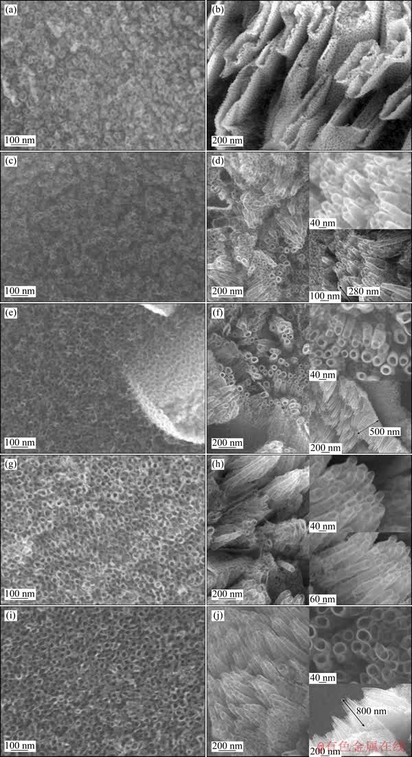
图2 阳极氧化不同时间后Cu-Ti-O纳米管阵列表面和侧面形貌FESEM像
Fig. 2 FESEM images of Cu-Ti-O nanotube arrays grown on Cu-rich phase for (a) 5 min, (c) 30 min, (e) 60 min, (g) 120 min, (i) 180 min and Ti-rich phase for (b) 5 min, (d) 30 min, (f) 60 min, (h) 120 min, (j) 180 min, respectively

图3 阳极氧化120和180 min制备的Cu-Ti-O纳米管阵列在O2气氛中经450 ℃退火2 h后的XRD谱
Fig. 3 XRD patterns of Cu-Ti-O nanotube arrays annealed in O2 at 450 ℃ for 2 h after anodized for 120 and 180 min
对比两组Cu-Ti-O纳米管阵列试样的XRD谱还可以发现,在O2气氛中450 ℃退火晶化2 h后,阳极氧化180 min制备的Cu-Ti-O纳米管中对应于锐钛矿(101)和金红石(110)特征衍射峰强度要明显强于阳极氧化120min制备的纳米管试样,这主要是由于阳极氧化时间较短时,Cu的溶解程度相对较低,经450 ℃的O2气氛退火晶化后,CuO晶粒能够大量存在于锐钛矿相晶粒之间,因而,在一定程度上降低了锐钛矿相晶粒之间的接触机率,阻碍了锐钛矿相晶粒的进一步生长,抑制了锐钛矿相因晶粒长大所产生的尺寸效应而引起的锐钛矿向金红石相的转变[27],因而金红石相转变量相对较低。而同样的现象在唐为华等[28]的报道中也出现过,作者发现,随着CuO生成量的增加,TiO2粒子间接触以及长大被阻碍,从而抑制了TiO2晶粒的聚集以及锐钛矿相的形成。
由于XRD通常反映的是试样中平均的组成和结构信息,很难准确区别出Cu-Ti-O纳米管阵列中的富Cu相和富Ti相的细微差别,因此,采用激光拉曼光谱分别对富Ti相和富Cu相区域内的Cu-Ti-O纳米管阵列进行成分表征。
图4所示为20V恒压阳极氧化120和180 min后生长的Cu-Ti-O纳米管阵列在O2气氛中450 ℃退火晶化2 h后富Ti相与富Cu相区域内Cu-Ti-O纳米管阵列的Raman谱。图4(a)所示为富Ti相区域内Cu-Ti-O纳米管的Raman谱。由图4(a)中可以看出,在阳极氧化120n和180 min后,在144、195、392、515和635 cm-1拉曼位移处分别出现了锐钛矿相的5个特征拉曼振动峰,分别对应于Eg、Eg、B1g、B2g和Eg振动模式。此外,对于20 V恒压阳极氧化180 min制备的Cu-Ti-O纳米管阵列而言,在437 cm-1拉曼位移附近还出现了一个弱的台阶状振动峰,如图4(a)中的放大图谱,此峰对应于金红石相Eg振动模式,表明20 V电压阳极氧化180 min后制备的Cu-Ti-O纳米管中发生了明显的锐钛矿向金红石相的转变过程,而这与图3的XRD结果高度一致。
图4(b)所示为富Cu相内Cu-Ti-O纳米管阵列在O2气氛中450 ℃退火晶化2 h后的Raman谱。由图4(b)中可以发现,富Cu相区域的Raman谱与富Ti相有明显区别,20 V阳极氧化120 min和180 min后,富Cu相区域内的Cu-Ti-O纳米管阵列在248和442cm-1拉曼位移处均出现了明显的金红石相的特征拉曼振动峰,分别对应于多声子和Eg振动模式,与富Ti相生长的Cu-Ti-O纳米管阵列相比,在O2气氛中经450 ℃退火晶化2 h后,富Cu相生长的Cu-Ti-O纳米管阵列中金红石相的振动峰强度要明显高于富Ti相的,这主要是由于在富Cu相内,由于Cu含量较高,更多的Cu能够进入到TiO2晶格并形成缺陷,在一定程度上促进了锐钛矿向金红石相的转变。此外,对比248和442 cm-1拉曼位移处对应于金红石相拉曼振动峰的强度可以发现,20 V阳极氧化180 min制备的Cu-Ti-O纳米管阵列的金红石相拉曼振动峰的强度要略高于阳极氧化120 min制备的Cu-Ti-O纳米管阵列的,表明其金红石转变量有所增加,这也与图3的XRD结果高度一致。

图4 阳极氧化120和180 min制备的Cu-Ti-O纳米管阵列在O2气氛中450 ℃退火2 h后Raman谱
Fig. 4 Raman spectra of Cu-Ti-O nanotube arrays annealed in O2 at 450 ℃ for 2 h after anodized for 120 and 180 min on Ti-rich (a) and Cu-rich (b) phases
此外,在富Cu相的Raman谱中,在约337 cm-1拉曼位移处还存在一个弱的振动峰,如图4(b)中的放大图谱所示,此峰对应于CuO的特征拉曼振动峰。在体材CuO的Raman谱中,CuO有3个活性拉曼振动峰,分别位于298 cm-1(Ag)、345 cm-1(Bg)和632 cm-1(Bg)位移处[29]。在富Ti相内,并没有观察到CuO在上面3个拉曼位移处存在明显的拉曼振动峰,如图4(a)所示。相反,在富Cu相内,如图4(b)所示,在337 cm-1拉曼位移处存在一个微弱的拉曼振动峰,此峰对应于CuO的Bg振动模式,但相对于体材CuO来说,此峰有非常明显的蓝移趋势,这主要是由晶粒尺寸效应引起的。在XU等[30]的报道中,当CuO晶粒尺寸由大于100 nm减小到30 nm和10 nm时,CuO的特征拉曼振动峰会明显地向低频拉曼移动(342 cm-1→341 cm-1→330 cm-1),即蓝移。
2.3 XPS分析
图5所示为20 V恒压阳极氧化120 min和180 min制备的Cu-Ti-O纳米管表面Cu2p、Ti2p和O1s的XPS谱。由图5(a)和(a′)可以看出,在O2气氛450℃退火晶化2 h后,两组试样的Cu2p图谱经过高斯-洛伦兹拟合以后在结合能为932.9和953.2 eV位置均存在两个XPS谱峰,它们分别对应于Cu2p3/2和Cu2p1/2[31],表明Cu-Ti-O纳米管阵列中存在一部分CuO,这与图2的XRD谱和图3的Raman结果相一致。
此外,在Cu2p的XPS谱中,结合能在942 eV附件还存在一个较强的谱峰,此峰对应于CuO震激伴峰,与Cu2p3/2峰位置相距10 eV。曹立礼[32]指出,CuO表面XPS谱的明显特点就是光电子出射时有震激过程,在Cu2p3/2谱峰高结合能一侧约7~10 eV会出现非常明显的震激伴峰,其结果不仅改变Cu2p3/2峰位和峰形,其强度接近Cu2p3/2主峰。此震激伴峰的出现更进一步表明在Cu-Ti-O纳米管阵列表面生成一部分CuO晶粒,这与图3的XRD谱和图4的Raman结果高度一致。而对于零价态Cu,其XPS谱上则不存在震激伴峰,对于Cu2O其XPS图谱上仅存在十分微弱的伴峰结构。在LI等[33]报道的Cu2O/Cu/TiO2纳米管中,Cu2p的XPS图谱中没有观察到对应于CuO震激伴峰的出现,同样,在TREJO-TZAB等[34]的报道中,在Cu2p的XPS图谱上仅观察到位于935.2 eV和952.0 eV附近的XPS谱峰,作者将其归因于Cu2O和金属Cu的出现。因此,XPS谱有震激伴峰的存在为识别铜的化学态提供了有力的依据。

图5 阳极氧化120和180 min制备的Cu-Ti-O纳米管阵列在O2气氛中450 ℃退火2 h后Cup, Ti2p和O1s的XPS谱
Fig. 5 XPS spectra of Cu2p ((a), (a′)), Ti2p ((b), (b′)) and O1s ((c), (c′)) on surface of Cu-Ti-O nanotube arrays annealed in O2 at 450 ℃ for 2 h after anodized for 120 ((a), (b), (c)) and 180 (a′), (b′), (c′) min
由图5(b)和(b′)可看出,Ti2p3/2和Ti2p1/2峰分别位于(458.45±0.15) eV和(464.1±0.1) eV结合能处,其结合能差距为(5.7±0.05) eV,均处于标准范围以内且二者峰形且呈Gauss对称分布,即Ti是由单一态所组成[35]。这表明Ti离子仍旧处于氧八面体的环境中。此外,由于Ti2+或Ti0的结合能比Ti4+的小3 eV以上,而Ti3+离子的结合能约为457.4 eV,这也进一步表明TiO2纳米管表面的Ti原子为完全氧化状态(O―Ti―O),即对应于TiO2晶格中Ti4+氧化态[36]。
由图5(c)和(c′)可看出,两组试样的XPS图谱中均存在3个拟合峰,中心位置分别位于529.6、531.5和532.8 eV处,分别对应于晶格氧(OL, 530.3 eV)、表面羟基氧(O―OH, 532.1 eV)和原子吸附氧(OS, 533.6 eV)[37]。通常,积分面积的大小可用来表示相对含量的高低,因此,通过对比O1s拟合峰面积,可以发现经20 V阳极氧化120 min制备的Cu―Ti―O纳米管阵列表面羟基氧浓度要高于20 V阳极氧化180 min制备的Cu―Ti―O纳米管阵列。
2.4 UV-vis-DRS结果
图6所示为Cu-Ti-O与未经掺杂的TiO2纳米管阵列在O2气氛中450 ℃退火晶化2 h后的UV-vis-DRS谱。由图6中可以看出,Cu掺杂后TiO2纳米管阵列的UV-vis吸收图谱有明显不同。通常,TiO2纳米管阵列的吸收带边可由直线外推法得到[38],由此得到20V恒压阳极氧化120 min和180 min后制备的未经掺杂的TiO2纳米管阵列,在O2气氛中450 ℃退火2 h的本征吸收带边均为450 nm,而20 V阳极氧化120 min和180 min后制备的Cu-Ti-O纳米管阵列的本征吸收带边分别红移至467 nm和473 nm。由于掺杂所引起的缺陷以及由此导致的晶相组成的变化[39-40]均对TiO2纳米管阵列的吸收带边的有直接影响,而Cu掺杂后促进了TiO2纳米管中锐钛矿向金红石相的转变,因而,在一定程度上有利于拓展TiO2的本征吸收带边,即红移。
对比未经掺杂的TiO2纳米管阵列,20V阳极氧化120和180 min制备的Cu-T-O纳米管阵列在50~600 nm可见光波长范围内吸收强度明显增强,这主要是由于Cu-Ti-O纳米管中一部分CuO生成的结果。作为p型半导体,CuO的吸收带边为727 nm,通过直线外推法,得到经20 V阳极氧化120和180 min制备的Cu-T-O纳米管阵列,经O2气氛450 ℃退火2 h后在450~600 nm可见,光波长范围内的吸收带边分别为763和727 nm。
由图6还可以看出,在20V电压下阳极氧化180 min制备的未经掺杂的TiO2和Cu-Ti-O纳米管阵列在波长小于550 nm区域内均表现出更强的吸收,ZHUANG等[41]在类似的报道中也指出,对于未经掺杂的TiO2纳米管阵列而言,当纳米管长度增加时,纳米管阵列中TiO2含量增加,其UV-vis吸收强度增强;另一方面,Cu-Ti-O纳米管阵列中CuO含量对其吸收带边也有着重要影响。随着阳极氧化时间的延长,在20 V阳极氧化180 min制备的Cu-Ti-O纳米管阵列中Cu的溶解程度增大,在O2气氛中450 ℃退火2 h后,CuO晶粒减少,因而,阳极氧化180 min制备的Cu-Ti-O纳米管的吸收带边相比阳极氧化120 min制备的Cu-Ti-O纳米管有所蓝移。

图6 阳极氧化120和180 min制备的Cu-Ti-O纳米管阵列在O2气氛经450 ℃退火2 h后UV-vis-DRS曲线
Fig. 6 UV-vis-DRS curves of Cu-Ti-O and TiO2 nanotube arrays annealed in O2 at 450 ℃ for 2 h after anodized for 120 and 180 min
3 结论
1) 通过阳极氧化,在Cu30-Ti70合金基体上成功制备出Cu掺杂Cu-Ti-O纳米管阵列。
2) Cu掺杂所产生的氧空位在一定程度上促进了锐钛矿向金红石相的转变,而随着阳极氧化时间的延长,富Ti相区域内Cu-Ti-O纳米管管长增加、管壁厚度减薄、晶粒生长和尺寸效应加速了Cu-Ti-O纳米管阵列锐钛矿向金红石相的转变。
3) Cu掺杂成功拓展了Cu-Ti-O纳米管阵列的禁带宽度,在20V恒压下,阳极氧化120和180 min后制备的Cu-Ti-O纳米管阵列在可见光范围内的吸收带边分别为763和727 nm。
4) Cu-Ti-O纳米管阵列的光电化学性能以及Cu掺杂浓度对Cu-Ti-O纳米管阵列形貌、结构和性能影响规律也将会继续深入研究。
REFERENCES
[1] LIU L I, CHEN S G, SUN W W, XIN J W. Enhancing the visible light absorption via combinational doping of TiO2 with nitrogen (N) and chromium (Cr)[J]. Journal of Molecular Structure, 2011, 1001: 23-28.
[2]  M, VOJVODIC A, ABILD-PEDERSEN F,
  J K. Electronic origin of the surface reactivity of transition-metal-doped TiO2(110)[J]. The Journal of Physical Chemistry C, 2013, 117 (1): 460-465.
[3] DUKES F M, IUPPA E, MEYER B, SHULTZ M J. Differing photo-oxidation mechanisms: Electron transfer in TiO2 versus iron-doped TiO2[J]. Langmuir, 2012, 28(49): 16933-16940.
[4] OHNO T, MITSUI T, MATSUMURA M. Photocatalytic activity of S-doped TiO2 photocatalyst under visible light[J]. Chemistry Letters, 2003, 32(4): 364-365.
[5] KIRAN V, SAMPATH S. Enhanced Raman spectroscopy of molecules adsorbed on Carbon-doped TiO2 obtained from Titanium carbide: A visible-light-assisted renewable substrate[J]. ACS Applied Materials & Interfaces, 2012, 4(8): 3818-3828.
[6] XU H, ZHANG L Z. Selective nonaqueous synthesis of C-Cl-codoped TiO2 with visible-light photocatalytic activity[J]. The Journal of Physical Chemistry C, 2010, 114(26): 11534-11541.
[7] MUSA A O, AKOMOLAFE T, CARTER M J. Production of cuprous oxide, a solar cell material, by thermal oxidation and a study of its physical and electrical properties[J]. Solar Energy Materials and Solar Cells, 1998, 51(3/4): 305-316.
[8] XIAO P, GARCIA B B, GUO Q, LIU D W, CAO G Z. TiO2 nanotube arrays fabricated by anodization in different electrolytes for biosensing[J]. Electrochemistry Communications, 2007, 9(9): 2441-2447.
[9] KANG T S, SMITH A P, TAYLOR B E, DURSTOCK M F. Fabrication of highly-ordered TiO2 nanotube arrays and their use in dye-sensitized solar cells[J]. Nano Letters, 2009, 9(2): 601-606.
[10] TSAI C C, TENG H S. Regulation of the physical characteristics of titania nanotube aggregates synthesized from hydrothermal treatment[J]. Chemistry of Materials, 2004, 16(22): 4352-4358.
[11] SANDER M S, COTE M J, GU W, KILE B M, TRIPP C P. Template-assisted fabrication of dense, aligned arrays of titania nanotubes with well-controlled dimensions on substrate[J]. Advanced Materials, 2004, 16(22): 2052-2057.
[12] GONG D, GRIMES C A, VARGHESE O K, HU W C, SINGH R S, CHEN Z, DICKEY E C. Titanium oxide nanotube arrays prepared by anodic oxidation[J]. Journal of Materials Research, 2001, 16(12): 3331-3334.
[13] 王泽高, 郑树楠, 贾春阳, 延 卫. Cu掺杂TiO2及其纳米管的制备、表征与光催化性能[J]. 无机化学学报, 2010, 26(5): 875-878.
WANG Ze-gao, ZHENG Shu-nan, JIA Chun-yang, YAN Wei. Preparation, structure characterization and photocatalytic performance of Cu doped TiO2 nanopowder and its corresponding nanotube[J]. Chinese Journal of Inorganic Chemistry, 2010, 26(5): 875-878.
[14] MOR G K, VARGHESE O K, WILKE R H T, SHARMA S, SHANKAR K, LATEMPA T J, CHOI K S, GRIMES C A. p-type Cu-Ti-O nanotube arrays and their use in self-biased heterojunction photoelectrochemical diodes for hydrogen generation[J]. Nano Letters, 2008, 8(7): 1906-1911.
[15] MOR G K, PRAKASAM H E, VARGHESE O K, SHANKAR K, GRIMES C A. Vertically oriented Ti-Fe-O nanotube array films: Toward a useful material architecture for solar spectrum water photoelectrolysis[J]. Nano Letters, 2007, 7(8): 2356-2364.
[16] KIM W G, CHOE H C, KO Y M, BRANTLEY W A. Nanotube morphology changes for Ti-Zr alloys as Zr content increases[J]. Thin Solid Films, 2009, 517(17): 5033-5037.
[17] TSUCHIYA H, AKAKI T, NAKATA J, TERADA D, TSUJI N, KOIZUMI Y, MINAMINO Y, SCHMUKI P, FUJIMOTO S. Anodic oxide nanotube layers on Ti-Ta alloys: Substrate composition, microstructure and self-organization on two-size scales[J]. Corrosion Science, 2009, 51(7): 1528-1533.
[18] FENG X J, MACAK J M, ALBU S P, SCHMUKI P. Electrochemical formation of self-organized anodic nanotube coating on Ti-28Zr-8Nb biomedical alloy surface[J]. Acta Biomaterialia, 2008, 4(2): 318-323.
[19] TSUCHIYA H, MACAK J M, GHICOV A, TANG Y C, FUJIMOTO S, NIINOMI M, NODA T, SCHMUKI P. Nanotube oxide coating on Ti-29Nb-13Ta-4.6Zr alloy prepared by self-organizing anodization[J]. Electrochimica Acta, 2006, 52(1): 94-101.
[20] MA Q, LIU S J, WENG L Q, LIU Y, LIU B. Growth, structure and photocatalytic properties of hierarchical Cu-Ti-O nanotube arrays by anodization[J]. Journal of Alloys and Compounds, 2010, 501(2): 333-338.
[21] LUO B M, YANG H B, LIU S K, FU W Y, SUN P, YUAN M X, ZHANG Y Y, LIU Z L. Fabrication and characterization of self-organized mixed oxide nanotube arrays by electrochemical anodization of Ti-6Al-4V alloy[J]. Materials Letters, 2008, 62(30): 4512-4515.
[22] MOHAPATRA S K, RAJA K S, MISRA M, MAHAJAN V K, AHMADIAN M. Synthesis of self-organized mixed oxide nanotubes by sonoelectrochemical anodization of Ti-8Mn alloy[J]. Electrochimica Acta, 2007, 53(2): 590-597.
[23] MA Q, LIU S J. Significantly enhanced structural and thermal stability of anodized anatase nanotube arrays induced by tensile strain[J]. Electrochimica Acta, 2011, 56(22): 7596-7601.
[24] XIN B F, WANG P, DING D D, LIU J, REN Z Y, FU H G. Effect of surface species on Cu-TiO2 photocatalytic activity[J]. Applied Surface Science, 2008, 254(9): 2569-2574.
[25] 辛柏福, 井立强, 付宏刚, 孙志华, 任志宇, 王百齐, 蔡伟民. 掺杂Cu的TiO2纳米粒子的制备、表征及其光催化活性[J]. 高等学校化学学报, 2004, 25(6): 1076-1080.
XIN Bai-fu, JING Li-qiang, FU Hong-gang, SUN Zhi-hua, REN Zhi-yu, WANG Bai-qi, CAI Wei-min. Preparation and characterization of Cu doped TiO2 nanoparticles and their photocatalytic activity[J]. Chemical Research in Chinese Universities, 2004, 25(6): 1076-1080.
[26] 宁成云, 王玉强, 郑华德, 谭帼馨, 陈晓峰, 马 强, 刘绪建. Cu掺杂二氧化钛纳米管阵列的研究[J]. 硅酸盐通报, 2009, 28(4): 775-778.
NING Cheng-yun, WANG Yu-qiang, ZHENG Hua-de, TAN Guo-xin, CHEN Xiao-feng, MA Qiang, LIU Xu-jian. Research on Cu-doped TiO2 nanotube arrays[J]. Bulletin of Chinese Ceramic Society, 2009, 28(4): 775-778.
[27] LEE H J, HAHN S H, KIM E J, YOU Y Z. Influence of calcination temperature on structural and optical properties of TiO2-SiO2 thin films prepared by sol-gel dip coating[J]. Journal of Materials Science, 2004, 39(11): 3683-3688.
[28] 徐 蕙, 王顺利, 刘爱萍, 陈本永, 唐为华. Cu/TiOx复合薄膜的电子态分析及其对亲水性的影响[J]. 物理学报, 2010, 59(15): 3601-3606.
XU Hui, WANG Shun-li, LIU Ai-ping, CHEN Ben-yong, TANG Wei-hua. Electronic state and its effect on the hydrophilicity of Cu/TiOx composite films[J]. Acta Physica Sinica, 2010, 59(15): 3601-3606.
[29] REIMANN K, SYASSEN K. Pressure dependence of Raman modes in CuO[J]. Solid State Communications, 1990, 76(2): 137-140.
[30] XU J F, JI W, SHEN Z X, LI W S, TANG S H, YE X R, JIA D Z, XIN X Q. Raman spectra of CuO nanocrystals[J]. Journal of Raman Spectroscopy, 1999, 30(5): 413-415.
[31] FU M, LI Y L, WU S W, LU P, LIU J, DONG F. Sol-gel preparation and enhanced photocatalytic performance of Cu-doped ZnO nanoparticles[J]. Applied Surface Science, 2011, 258(4): 1587-1591.
[32] 曹立礼. 材料表面化学[M]. 北京: 清华大学出版社, 2007: 254.
CAO Li-li. Materials surface chemistry[M]. Beijing: Tsinghua University Press, 2007: 254.
[33] LI Z H, LIU J W, WANG D J, GAO Y, SHEN J. Cu2O/Cu/TiO2 nanotube ohmic heterojunction arrays with enhanced photocatalytic hydrogen production activity[J]. International Journal of Hydrogen Energy, 2012, 37(8): 6431-6437.
[34] TREJO-TZAB R, ALVARADO-GIL J J, QUINTANA P,  P. N-doped TiO2 P25/Cu powder obtained using nitrogen (N2) gas plasma[J]. Catalysis Today, 2012, 193: 179-185.
[35] ZHANG Z, GOODALL J B M, MORGAN D J, BROWN S, CLARK R J H, KNOWLES J C, MORDAN N J, EVANS J R G, CARLEY A F, BOWKER M, DARR J A. Photocatalytic activities of N-doped nano-titanias and titanium nitride[J]. Journal of the European Ceramic Society, 2009, 29(11): 2343-2353.
[36] GAO B F, MA Y, CAO Y A, ZHAO J C, YAO J N. Effect of ultraviolet irradiation on crystallization behavior and surface microstructure of titania in the sol-gel process[J]. Journal of Solid State Chemistry, 2006, 179(1): 41-48.
[37] POZNYSK S K, PERGUSHOV V I, KOKORIN A I, KULAK A I, SCHLPAFER C W. Structure and electrochemical properties of species formed as a result of Cu(II) ion adsorption onto TiO2 nanoparticles[J]. The Journal of Physical Chemistry B, 1999, 103(8): 1308-1315.
[38] RETUERT J, OUIJADA A, AREAS V. Porous titania obtained through polymer incorporated composites[J]. Chemistry of Materials, 1998, 10(12): 3923-3927.
[39] LAI Y K, HUANG J Y, ZHANG H F, SUBRAMANIAM V P, TANG Y X, GONG D G, SUNDAR L, SUN L, CHEN Z, LIN C J. Nitrogen-doped TiO2 nanotube array films with enhanced photocatalytic activity under various light sources[J]. Journal of Hazardous Materials, 2010, 184(1/3): 855-863.
[40] LIU M, QIU X Q, MIYAUCHI M, HASHIMOTO K. Cu(II) oxide amorphous nanoclusters grafted Ti3+ self-doped TiO2: An efficient visible light photocatalyst[J]. Chemistry of Materials, 2011, 23(23): 5282-5286.
[41] ZHUANG H F, LIN C J, LAI Y K, SUN L, LI J. Some critical structure factors of titanium oxide nanotube array in its photocatalytic activity[J]. Environmental Science and Technology, 2007, 41(13): 4735-4740.
(编辑 李艳红)
基金项目:国家自然科学基金资助项目(51302150,51172053);深圳市基础研究计划项目(JCYJ20130401173600792)
收稿日期:2013-03-11;修订日期:2014-09-08
通信作者:刘绍军,副教授,博士;电话:0731-88876135;传真:0731-88710855;E-mail:shaojunliu@gmail.com

