Modeling of photolithography process in semiconductor wafer fabrication systems using extended hybrid Petri nets
来源期刊:中南大学学报(英文版)2007年第3期
论文作者:周炳海 潘青枝 王世进 吴斌
文章页码:393 - 398
Key words:semiconductor wafer fabrication; photolithography process; hybrid Petri net; object-oriented method
Abstract: To describe a semiconductor wafer fabrication flow availably, a new modeling method of extended hybrid Petri nets (EHPNs) was proposed. To model the discrete part and continuous part of a complex photolithography process, hybrid Petri nets (HPNs) were introduced. To cope with the complexity of a photolithography process, object-oriented methods such as encapsulation and classifications were integrated with HPN models. EHPN definitions were presented on the basis of HPN models and object-oriented methods. Object-oriented hybrid Petri subnet models were developed for each typical physical object and an EHPN modeling procedure steps were structured. To demonstrate the feasibility and validity of the proposed modeling method, a real wafer photolithography case was used to illustrate the modeling procedure. The modeling results indicate that the EHPNs can deal with the dynamic modeling of a complex photolithography process effectively.
基金信息:the National Natural Science Foundation of China
J. Cent. South Univ. Technol. (2007)03-0393-06
DOI: 10.1007/s11771-007-0077-1
![]()
ZHOU Bing-hai(周炳海), PAN Qing-zhi(潘青枝), WANG Shi-jin(王世进), WU Bin(吴 斌)
(School of Mechanical Engineering, Shanghai Jiaotong University, Shanghai 200030, China)
Abstract: To describe a semiconductor wafer fabrication flow availably, a new modeling method of extended hybrid Petri nets (EHPNs) was proposed. To model the discrete part and continuous part of a complex photolithography process, hybrid Petri nets (HPNs) were introduced. To cope with the complexity of a photolithography process, object-oriented methods such as encapsulation and classifications were integrated with HPN models. EHPN definitions were presented on the basis of HPN models and object-oriented methods. Object-oriented hybrid Petri subnet models were developed for each typical physical object and an EHPN modeling procedure steps were structured. To demonstrate the feasibility and validity of the proposed modeling method, a real wafer photolithography case was used to illustrate the modeling procedure. The modeling results indicate that the EHPNs can deal with the dynamic modeling of a complex photolithography process effectively.
Key words: semiconductor wafer fabrication; photolithography process; hybrid Petri net; object-oriented method
1 Introduction
Semiconductor wafer fabrication is one of the most complex technological processes in this world. In general, the fabrication flow can be categorized into six areas[1]: diffusion, etching, implant, lithography, thin-film and inspection. Photolithography is usually the bottleneck process with the most expensive equipment in a wafer fabrication system[2]. A photolithography process is a complex and reentrant process and has over a hundred of processing steps. The time in the photolithography for the wafer’s fabrication is about 40%-50% of the total processing time[3]. Therefore, to describe a semiconductor wafer fabrication flow availably, it is very necessary for modeling a complex photolithography process.
In recent years, modeling study of a complex photolithography process has attracted attention increasingly[3]. Several modeling methods have been proposed to represent a discrete part of photolithography processes. Among them, Petri nets are now considered as a powerful tool especially suitable for systems that exhibit concurrency, conflicts, synchronization, etc.[4-8]. However, they do not provide the needed modularity required to represent complex systems made up of many interacting hybrid systems[9-10]. In order to overcome the weaknesses mentioned above, ALLAM et al[11] introduced hybrid Petri nets to modeling the semiconductor fabrication flow. Although all the large size entities are modeled in a continuous way with this approach, the model of the fabrication flow is still very complex. LEE et al[12] and HONG et al[13] introduced object-oriented approaches to PN-based modeling, and developed object-oriented high-level Petri nets (OPNets). HSIUNG et al[14] LIU et al[15] extended the OPNet to an extended object-oriented Petri nets (EOPNs) paradigm. Both OPNets and EOPNs models are more compact and consequently more manageable. However, the existing OPNs models are not powerful enough to cope with the complex hybrid wafer fabrication process. To model the photolithography process effectively, hybrid Petri nets, which combine a discrete part and a continuous part, were introduced in this study. And the extended hybrid Petri nets (EHPNs) were presented to model a complex photolithography process.
2 Photolithography process
A photolithography process is the process of transferring geometric shapes on a mask to the surface of a silicon wafer[16]. The basic photolithographic sequence is shown in Fig.1. The first photolithography operation is to clean particulate matter on the surface as well as any traces of organic, ionic, and metallic impurities. The second operation is to coat wafers with photo-resist. The wafers are then baked to firm the photo-resist and improve their adhesion to the wafers before they are sent to aligners or steppers for exposure. In the case of a stepper, a reticle, a template containing the pattern for only a few chips, is placed on the wafer and exposed to ultraviolet (UV) light. The alignment and exposure process, which constitutes a step, is repeated until the whole wafer surface is exposed. Each layer requires a different mask specifically designed for that layer’s device characteristics. The wafers are then sent for developing, where the exposed photo-resist is removed with a special solvent, after which it goes through the final bake to ensure that the unexposed photo-resist adheres to the wafers. Once these steps are completed, the lot typical is moved to post-photolithography analytical operations.
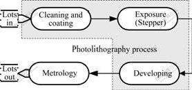
Fig.1 Simplified photolithography process flow
According to the descriptions mentioned above, the photolithography process includes a discrete part (e.g. wafer baked process) and a continuous part (e.g. wafer exposure process). The discrete modeling method cannot be used to cope with a hybrid process precisely. The modeling method must be provided the ability to deal with a hybrid complex process.
3 Extended hybrid Petri nets
Hybrid Petri net is a powerful tool for modeling hybrid systems. This model inherits all the advantages of the Petri net model[11]. Based on the hybrid Petri nets, to model a photolithography process compactly, object- oriented methods are integrated to the hybrid Petri nets. From the view of object-oriented viewpoint, a process/system is composed of physical objects and their interconnection relations. An extended hybrid Petri net (EHPN) was developed according to this conception, i.e., an EHPN consists of two parts:
EHPN =(O, R)
where O={O1, O2, …, On} is a set of finite physical object places in a photolithography process, in which Oi, (i = 1, 2,…, n) is a physical object place in an EHPN model corresponding to a physical object that is described by an encapsulated hybrid Petri net; R is a set of communicating relations between physical objects that are described by message places between physical object subnets.
3.1 Physical object subnet
A physical object subnet is defined as a 7-tuple:
Oi=(Pi, Ti, hi, τi, Fi, Ci,![]() )
)
where Pi=DPi∪CPi∪MPi is the set of finite places, in which DPi is a set of finite discrete places, CPi is a set of finite continuous places, MPi is a set of finite message places. A continuous place is represented in a drawing as two concentric circles. MPi is the union of IMPi and OMPi that are the sets of finite input message places and output message places respectively. A message place is represented in a drawing as an ellipse.
Ti=DTi ∪CTi ∪MTi is a non empty set of finite transitions. DTi is a set of finite discrete transitions, and CTi is a set of finite continuous transitions. A continuous transition is represented in a drawing as a hollow bar. MTi is a set of finite gates in a physical object Oi, where Pi∩Ti =Φ, Pi∪Ti ≠Φ.
hi: P∪T→{C, D} indicates for each node if it is a discrete (D) or a continuous (C) node.
τi : T→Γ+ associates with each transition of a positive real number dj, where the time delay associated with a D-transition tj is dj. The maximal firing speed associated with a C-transition tj is vj = l/dj.
Fi : Pi × Ti ∪Ti × Pi →{0 ,l} is a set of finite arcs between D-transitions (activity transitions)/C-transitions and discrete (message) /continuous places. Fi=FIi∪FOi, where FIi and FOi are input incidence mapping and output incidence mapping. FIi: Pi × Ti→Γ if h(pk)=D; Pi × Ti→Γ+ if h(pk)=C. FOi: Pi × Ti→Γ if h(pk)=D; Pi × Ti→Γ+ if h(pk)=C. FIi and FOi must meet the following conditions: if pk and tj are such that h(pk)=D and h(tj)=C , then FIi(pk,tj)=FOi(pk,tj) must be verified, where FIi(pk,tj) and FOi(pk,tj) are input and output flow from pk to tj . This ensures marking of D-places to be an integer whatever evaluation occurs.
Ci is a set of colored tokens in physical object Oi , Ci={C(DPi), C(CPi), C(IMPi), C(OMPi)}, where C(DPi) is a set of colored tokens associated with all the discrete places; C(CPi) is a set of colored tokens associated with all the continuous places; C(IMPi) is a set of colored tokens associated with all the input message places, and C(OMPi) is a set of colored tokens associated with all the output message places.
![]() is a set of initial markings of all state and message places inside Oi.
is a set of initial markings of all state and message places inside Oi.
The marking M(t)i of a physical object place Oi at time t can be deduced from marking ![]() at time O using the following fundamental equation:
at time O using the following fundamental equation:
![]()
where σ(t) represents the number of times that each D-transition has been fired (discrete interpretation) between initial time and time t. The components associated with C-transitions are equal to zero. The components of v(u) vector represent instantaneous firing speeds associated with C-transitions. D-transitions are equal to zero. This equation separates the discrete evolution from the continuous one. It represents a trajectory in the marking space. According to the approach considered for computing the instantaneous firing speed vector, many models have been proposed[9]. Here, only the constant speed continuous Petri net is considered.
3.2 Relations of physical objects
In an EHPN, the interconnection between the physical objects is depended on their message places of the objects (input message places and output message places), i.e. if MPi∩MPj ≠Φ, then the two physical object places Oi and Oj have message passing. The interconnection relations of physical objects at the system level may be realized by a set of gates. Mathematically, the interconnection of physical objects is defined as follows:
R={Rij, i, j = 1, 2, …, I, i ≠ j}
where Rij specifies the message passing relations between the sending physical object place Oi and the receiving physical object place Oj.
Rij={Gij, OYij, IYij, EMij}
where Gij is a set of finite special activity transitions called gates that are located between output message places OMPi of MPi and input message places IMPj of MPj . The union of all the gates associated with R is the set of gates in the system. OYij is a set of finite output connection arcs from OMPi of MPi to Gij; IYij is a set of finite input connection arcs from IMPj of MPj; EMij is a expression function of connection arcs between OMPi and IMPj:
EMij=[IYF(IYij ,Gij), OYF(OYij ,Gij)]
where IYF(IYij ,Gij) is the input expression function for an arc that connects gate Gij to the input message place IYij in the Oj; OYF(OYij ,Gij) is the output expression function for an arc that connects the output message place OYij in the Oi to gate Gij.
4 Developing of EHPN models
4.1 OHPN subnet models
As mentioned above, the photolithography is a typical complex hybrid process flow. In order to describe the development of EHPN models for a photolithography process, typical photolithography equipment is considered for building object-oriented hybrid Petri subnet (OHPN) models. In general, the typical photolithography equipment consists of a track system, stackers (STK), material handling equipment and exposure tools called steppers (STP). A track system is integrated equipment composed of scores of process modules, cassette indexers, and more than one transfer modules. The process modules are composed of cool plates (CP), hot plates (HP or HHP), post exposure bake hot plates (PEB), edge exposures (EE), spin coaters (SC), spin developers (SD), and low-pressure adhesions (LPAH)[17]. To establish OHPN subnet models of physical objects of the typical equipment, all physical objects of the typical equipment are mainly classified as three objects.
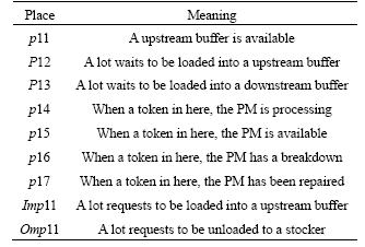
1) Processing machine object (PMO) represents a general photolithography processing machine (PM) such as steppers, hot plates, spin coaters, spin developers, and edge exposures. We assume that a PM has an upstream buffer from which the PM draws wafers (a lot) for processing. Before the PM starts processing, a minimal level of B wafers (a lot) in the upstream buffer is required. Therefore, the PM preparation process starts, taking certain duration. When the preparation operation is finished, the PM is allocated to the lot until all wafers have been processed. A PMO model abstracts the behavior of majority PMs. The PMO OHPN subnet is shown in Fig.2. Each place and transition have the meanings given in Tables 1-2.
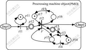
Fig.2 Object subnet model of PMO
Table 1 Meanings of places for PMO subnet
2) Transporter object (TSPO) represents material handling equipment objects (e.g. automatic guide vehicles―AGVs, overhead hoist transporters―OHTs, industrial robots―IR and operators) that transport wafers (lots) among stockers and processing machines. A TSPO model abstracts the behavior of majority transporting equipment. The TSPO OHPN subnet is shown in Fig.3. The meanings of each place and transition are similar to the meanings given in Tables 1-2.
Table 2 Meanings of transitions for PMO subnet
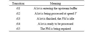
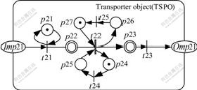
Fig.3 Object subnet model of TSPO
3) Stocker object (STKO) represents general stockers at the entrance/exit of each photolithography area, which automatically store and retrieve wafers (lots) that are waiting for processing, and ones that have finished processing in the current photolithography area. The STKO OHPN subnet is shown in Fig.4.
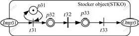
Fig.4 Object subnet model of STKO
4.2 EHPN models
Construction of an EHPN model is derived from the OHPN subnet models. First, each encapsulated OHPN subnet is represented as an object place and the message passing gate as an intelligent activity transition, the internal behavior (i.e., states of the OHPN subnet) of each physical object may be represented by the associated colored tokens. The procedure of constructing an EHPN model can be summarized as follows.
Step 1 Represent each encapsulated OHPN subnet as an object place Oi (i=1,2,… ,m).
Step 2 Represent each gate involved in an EHPN model as an intelligent activity transition Gj (j=1,2, …, n). An intelligent activity transition is connected with its input message places with an AND (OR) relation if it can be fired when all (some/any of) the connected message places have the required specific colored tokens. An intelligent activity transition is connected with its output message places with an AND (OR) relation if the colored tokens will be moved to all (some of) the connected message places.
Step 2.1 For any intelligent activity transition whose input―output connection is either an AND―OR or an AND―AND relation, it is represented as an ordinary intelligent activity transition.
Step 2.2 For any intelligent activity transition whose input―output connection is either an OR―OR or an OR―AND relation, it is represented as a hierarchical intelligent activity transition that may be further decomposed into one state place connected with one output and several input ordinary transitions to clarify the firing condition for a gate with OR input connections.
Step 3 Represent the [Oi―Gk―Oj] message passing relations specified in the process OHPN model, so that the properties of colored and timed Petri nets may be applied in the EHPN model.
Step 4 According to the process flow of each wafer lot type p (p=1,2, … ,P; P is the total number of wafer lot types), assign a colored token cr to represent its sub-process r (r=1,2, … ,wp; wp is the total number of sub-processes for wafer lot type p). For each sub-process r, identify the physical object that actually performs it.
Step 5 Based on the colored tokens and the allocated physical objects identified in Step 4, define the set of colored tokens, C(Oi)={cpi1,cpi2,…, cpiu}, associated with each object place Oi, and the time-delay attribute of colored token c.
Step 6 Check the EHPN models: see whether the EHPN reflects the photolithography process operation and modify the EHPN until it models the process accurately.
5 Case study
To illustrate the procedure of constructing an EHPN model, we consider a practical example based on actual data from semiconductor companies. The example of photolithography equipment layout is shown in Fig.5 for photolithography processes of 200 mm wafers[18]. Three transporters (robots) transfer wafers from process module to process module in each cell, or from cell to cell, and one transporter moves wafers from the track system to the expose tool and vice versa. There is one typical route for deep-UV processing: top anti-reflective coating (TARC). The route of TARC is given as follows:
TARC for deep UV processing: STK→HHP1→LPAH2→CP2→SC1→HP1→CP6→SC3→HP5→CP10→STP→PEB1→CP11→EE1→SD1→HP4→CP3→STK.
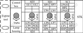
Fig.5 Layout of photolithography process
According to the proposed modeling method, EHPN model of photolithography process was built for the TARC example. The complete EHPN model for the example is described in Fig.6. It can be seen that the EHPN model has ten intelligent activity transitions (G11, G12, G21, G22, G31, G32, G41, G42, G51, G52) and twenty-one encapsulated object places ( e.g. OSTK, OCP2, OTSP1). The colored tokens associated with each object place, C(Oi) (i=1, 2, …, 21), which can be determined by grouping all the sub-processes performed by that object place’s corresponding equipment/resource, as shown in Table 3. Because the OR relation exists among the input message places and the output message places that are connected by intelligent activity transitions. The intelligent activity transitions are hierarchical intelligent activity transitions, such as G21, G31, G41, G42. Here, the G42 decomposition was merely represented. The internal behavior of G42 is shown in Fig.7. In order to describe hierarchical intelligent activity transitions how to be fired according colored token conditions, let consider a pair of colored tokens (e.g. c.23 and c.24) whose input and output are connected by the G42. Fig.8 illustrates the detail process flow of the colored token c.23 input into the G42 and the colored token c.24 output from the G42. Colored tokens allocated object places are OPEB1 and OTSP3 respectively. A conclusion can be drawn that intelligent activity G42 is used for connecting object place OPEB1 with colored token c.23 and OTSP3 with colored token c.24. It is clear that intelligent activity transition G42 can be enabled with respect to c.23 if there is a token c.23 in object place OPEB1 and the firing of G42 will remove a token c.23 from OPEB1 and add a token c.24 to object place OTSP3. Here, due to limited space, the detailed procedure of constructing steps is omitted.
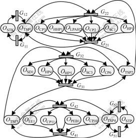
Fig.6 EHPN model of TARC process
Table 3 Process descriptions for TARC
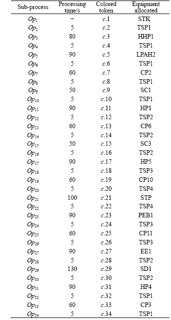
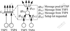
Fig.7 G42 decompositions of internal behavior
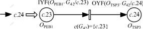
Fig.8 Constructing G42 fired transition
6 Conclusions
1) The EHPN is provided with the characteristics of object-oriented hybrid Petri nets, such as graphical representation, mathematical analysis capability of the control logic, discrete and continue descriptive capability, the high degree of modularity, flexibility, reusability, maintainability of the model.
2) To illustrate how to construct an EHPN model of a complex photolithography process, a case study is presented. The case study demonstrates that EHPNs can cope with the complexity for modeling a complex wafer photolithography process.
3) Since deadlock-free and conflict resolving strategies are very important for hybrid processes, the ongoing work includes the methods for detecting deadlocks and conflicts in an EHPN model.
References
[1] LIN J T, WANG F K, CHANG Y M. A hybrid push/pull dispatching rule for a photobay in a 300 mm wafer fab[J]. Robotics and Computer-Integrated Manufacturing, 2006, 22(1): 47-55.
[2] ZHOU M, JENG M D. Modeling, analysis, simulation, scheduling, and control of semiconductor manufacturing systems: A Petri net approach[J]. IEEE Transactions on Semiconductor Manufacturing, 1998, 11 (3): 333-357.
[3] AKCALT E, NEMOTO K, UZASOY R. Cycle-time improvements for photolithography process in semiconductor manufacturing[J]. IEEE Transactions on Semiconductor Manufacturing, 2001, 14 (1): 48-56.
[4] REISIQ W. Petri nets and algebraic specifications[J]. Theoretical Computer Science, 1991, 80(1): 1-34.
[5] LEE C C, LIN J T. Deadlock prediction and avoidance based on Petri nets for zone-control automated guided vehicle systems[J]. International Journal of Production Research, 1995, 33(12): 3249-3265.
[6] LIN M H, FU L C. Modeling, control and simulation of an IC wafer fabrication system: A generalized stochastic colored timed Petri net approach[J]. International Journal of Production Research, 2000, 38(14): 3305-3341.
[7] SALIMIFARD K, WRIGHT M. Petri net-based modeling of workflow systems: An overview[J]. European Journal of Operational Research, 2001, 134(3): 664-676.
[8] PARK J, REVELIOTIS S A, BODNER D A. High-fidelity rapid prototyping of 300 mm fabs through discrete event system modeling[J]. Computer in Industry, 2001, 45(1): 79-98.
[9] THEVENON L, FLAUS J M. Modular representation of complex hybrid systems: Application to the simulation of batch processes[J]. Simulation Practice and Theory, 2000, 8 (3): 283-306.
[10] JIANG Z, ZUO M J, FUNG R Y K. Performance modeling of complex dynamic production systems using temporized object-oriented Petri nets with changeable structure (TOPNs-CS)[J]. International Journal of Advanced Manufacturing Technology, 2000, 16(7): 521-536.
[11] ALLAM M, ALLA H. Modeling and simulation of an electronic component manufacturing system using hybrid Petri nets[J]. IEEE Transactions on Semiconductor Manufacturing, 1998, 11(3): 374-383.
[12] LEE Y K, PARK S J. OPNets: An object-oriented high-level Petri net model for real-time system modeling[J]. Journal of System Software, 1993, 20(1): 69-86.
[13] HONG J E, BAE D H. High-level Petri net for incremental analysis of object-oriented system requirements[J]. IEE Proceedings: Software, 2001, 148(1): 11-18.
[14] HSIUNG P A, LEE T Y, CHEN S H J. MOBnet: An extended Petri net model for the concurrent object-oriented system-level synthesis of multiprocessor systems[J]. IEICE Transactions on Information and Systems, 1997, E80-D(2): 232-242.
[15] LIU H, JIANG Z, FUNG R Y K. Modeling of large-scale complex re-entrant manufacturing systems by extended object-oriented Petri nets[J]. International Journal of Advanced Manufacturing Technology, 2005, 27(1/2): 190-204.
[16] GOSMAN B, SIVAN L S, SWISSA R. Yield enhancement in photolithography through model-based process control: Average mode control[J]. IEEE Transactions on Semiconductor Manufacturing, 2005, 18(1): 86-93.
[17] BRAUN A E. Track systems meet throughput and productivity challenges[J]. Semiconductor International, 1998, 21(2): 63-64.
[18] YOON H J, LEE D Y. Deadlock-free scheduling of photolithography equipment in semiconductor fabrication[J]. IEEE Transactions on Semiconductor Manufacturing, 2004, 17(1): 42-54.
Foundation item: Project(60574054) supported by the National Natural Science Foundation of China
Received date: 2006-11-24; Accepted date: 2007-01-10
Corresponding author: ZHOU Bing-hai, Associate professor; Tel: +86-21-62933460; E-mail: bhzhou@sjtu.edu.cn

