J. Cent. South Univ. (2012) 19: 1283-1289
DOI: 10.1007/s11771-012-1140-0
Low latency systolic multipliers for finite field GF(2m) based on irreducible polynomials
XIE Jia-feng(谢佳峰), HE Jian-jun(贺建军), GUI Wei-hua(桂卫华)
School of Information Science and Engineering, Central South University, Changsha 410083, China
? Central South University Press and Springer-Verlag Berlin Heidelberg 2012
Abstract: Systolic implementation of multiplication over GF(2m) is usually very efficient in area-time complexity, but its latency is usually very large. Thus, two low latency systolic multipliers over GF(2m) based on general irreducible polynomials and irreducible pentanomials are presented. First, a signal flow graph (SFG) is used to represent the algorithm for multiplication over GF(2m). Then, the two low latency systolic structures for multiplications over GF(2m) based on general irreducible polynomials and pentanomials are presented from the SFG by suitable cut-set retiming, respectively. Analysis indicates that the proposed two low latency designs involve at least one-third less area-delay product when compared with the existing designs. To the authors’ knowledge, the time-complexity of the structures is the lowest found in literature for systolic GF(2m) multipliers based on general irreducible polynomials and pentanomials. The proposed low latency designs are regular and modular, and therefore they are suitable for many time critical applications.
Key words: finite field; finite field multiplication; systolic structure; low latency; polynomials
1 Introduction
Finite field multiplication over GF(2m) is widely used in elliptic curve cryptography (ECC), transform computing and error control coding systems [1-2], in these years. The multiplication over GF(2m) is much more complex than the addition operation in finite fields [3-4]. Besides, the multiplication operation can be extended further to obtain the operations of division, exponentiation, and inversion [5-6]. The multiplication over GF(2m) can be easily implemented on a general purpose machine. But the software implementations usually do not meet the speed requirement of some time critical applications. Most of the real time applications, therefore, need hardware implementations. The hardware implementation usually has high cost in terms of area and time complexity. Therefore, the designing of a high-speed hardware structure with less area requirement has become much more demanding.
The choice of basis used to represent field elements can determine the performance of the field arithmetic. The finite field elements can be represented in various bases, namely the normal basis, polynomial basis and dual basis. Among them, the polynomial basis has lower design-complexity architecture for various applications than the other two representations owing to its features such as simplicity, regularity and modularity of the architecture. Therefore, the multiplications using polynomial basis representations are very efficient in comparison to the best methods for multiplication using the other two basis representations.
A number of works have been done on efficient realization of multiplication over GF(2m) based on irreducible polynomials [7-9]. These works can be classified into two types in terms of the design style: the systolic design and the non-systolic design [10-14]. The non-systolic design may have low latency, but its throughput is low, while the systolic design features modularity and regularity, which are important for the high-speed design [15-19]. All the processing elements (PEs) in a systolic array are fully pipelined, i.e., all communicating edges among the PEs contain delay elements, and the whole system usually contains only local interconnections [20]. But, there is one major disadvantage of the systolic design, namely, the latency of the systolic design is usually very large.
In an early work [7], a bit-parallel systolic design for multiplication over GF(2m) has been suggested by YEH et al. Then in Ref. [8], WANG and LIN suggested another efficient bit-parallel systolic design. But, for large values of m, these designs all need large number of logic gates and the latencies of these designs are too long. After that, several works have been suggested for efficient realization of finite field multiplication over GF(2m) [9-13]. But the latency of these designs is still too large. Recently, in Ref. [16], a systolic structure has been proposed for polynomial based multiplication, where the latency is m cycles. Then, in a recent work [17], MEHER suggested a systolic structure for multiplication over GF(2m) based on irreducible pentanomials, but the latency of the structure is still m cycles. Therefore, the designing of a low latency systolic structure for general irreducible polynomials and pentanomials has become much more interesting.
The systolic structures for multiplication over GF(2m) require efficient time complexity, especially when the designs are applied in real time environment. Most of the systolic designs, however, have latency ranging from m to 2m or even larger. And most of the systolic designs have critical path ranging from (TA+TX) to (TA+2TX) or even larger, where TA and TX denote the delay time of an AND gate and a XOR gate, respectively. Therefore, two low latency systolic designs for general irreducible polynomials and pentanomials will be presented in this work. A novel decomposition is used to express the former multiplier into two parallel units. Then, by suitable cut-set retiming, two systolic structures are derived from the signal flow graph (SFG).
2 Algorithm and proposed structures
2.1 Algorithm
Let f(x) be a m-degree irreducible polynomial over GF(2) in the form of
 (1)
(1)
where fi∈GF(2) = {0, 1}.
Then, the set {1, x, …, xm-1} is the polynomial basis in GF(2m), and any element in GF(2m) defined by f(x) is
 (2)
(2)
where ai∈GF(2).
Let a(x) and b(x) be two field elements and c(x) be the product, then
 (3)
(3)
where

and bi∈GF(2), for i = 0, 1,…, m-1.
Then, Eq. (3) can be expressed as another form [17]:
 (4)
(4)
Then, Eq. (4) can be changed into
 (5)
(5)
Then define
 (6)
(6)
Then
 (7)
(7)
Define that
 (8)
(8)
One can have
 (9)
(9)
Substituting Eq. (9) into Eq. (7),
 (10)
(10)
where
 (11)
(11)
The algorithm above is also called the classical “shift-and-add” algorithm [17], and then two systolic structures will be presented if we make a modification on the above algorithm.
Following the algorithms depicted above, two proposed low latency designs are derived.
2.2 Proposed design for general irreducible polynomials
Let f(x) be an irreducible polynomial in the form of
 (12)
(12)
where 1 = k1 <…< kt < m.
Comparing Eq. (12) with Eq. (1), one can find some (fi) are “0”, and some (fi) are “1”. Note that Eq. (11) can be performed recursively. Then, a SFG can be used for efficient representation of Eq. (5) and Eq. (11) as shown in Fig. 1, where it consists of m cells A, (m-1) cells M and (m-1) cells R. The functions of cell R, cell A and cell M are shown in Figs. 1(b), (c), and (d), respectively. The cell A performs the bit multiplication operation, and the cell M performs the bit addition operation, while the cell R performs the degree-reduction operation, according to Eq. (10) and Eq. (11). For example, the cell R1 performs the degree-reduction operation, such that the output of cell R1 is a(x)1, as shown in Fig. 1(a).
To derive a low latency systolic structure, first of all, (m/2) can be assumed as an integer, just for simplicity of discussion. Using Eq. (7), then Eq. (5) can be rewritten as

 (13)
(13)
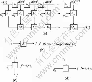
Fig. 1 Signal flow graph (SFG): (a) SFG; (b) Function of cell R; (c) Function of cell A; (d) Function of cell M
Then, one can have the SFG for Eq. (13), as shown in Fig. 2, where the final cell AC denotes the addition-cell (AC). It can be seen that the former SFG is decomposed into two sub-SFGs, where each sub-SFG is similar to that of Fig. 1. Note that functions of the cells in Fig. 2 are the same as those in Fig. 1. The AC just performs the addition operation, as shown in Fig. 2(b). To derive the proposed systolic structure from the SFG of Fig. 2, we can use the cut-set retiming, as shown in Fig. 3(a), where we introduce a delay between the cell R and the corresponding cell A and cell M. Also, the formation of the PEs is shown in Fig. 3(b), where a regular PE may contain two cells R, one cell A and one cell M. Note that the output of the two cells R will be used in the next PE, so that a critical path of a PE will be reduced significantly. The time required by the cell R, cell A, and cell M is defined as TCR, TCA, and TCM, respectively. Therefore, the critical path in a PE, accordingly, will be max{2TCR, (TCM+TCA)}, although the last PEs of the two sub-SFGs have critical path of (TCM+TCA).

Fig. 2 Proposed SFG
Fig. 3 Cut-set retiming of proposed SFG: (a) Cut-set; (b) Formation of PE
The proposed low latency systolic structure for multiplication over GF(2m) based on general irreducible polynomial is shown in Fig. 4. The structure of Fig. 4 consists of two systolic arrays, where each systolic array consists of (m/2) PEs. Besides, a Pr-PE and an AC are also required for the whole structure. It can be seen that the even number bits of operand b(x) are fed to the each PE of systolic array-1, respectively, while the odd number bits of operand b(x) are fed to each PE of systolic array-2, respectively. For example, b0 and b2 are fed to the PE0 and PE2, respectively, while b1 and b3 are fed to the PE1 and PE3, respectively. The functions of the PEs are shown in Figs. 4(b), (c), (d), (e) and (f), respectively. The input operand a(x) is fed to Pr-PE from left and the Pr-PE yields the outputs to the two systolic arrays separately. The PE0 and PE1 just perform the double degree-reduction operation (two R cells are contained in the PE, see Fig. 3), such that a(x)j+2 can be obtained from a(x)j. Also, a bit multiplication operation is required for the PE0 and PE1. The PE2 to PE(m-1) are the regular PEs, and the regular PE not only performs the double degree-reduction operation and the bit multiplication operation, but also the bit addition operation. Both the last PEs (from left) of the two systolic arrays only perform the bit multiplication operation and the bit addition operation. The final AC performs the addition operation.
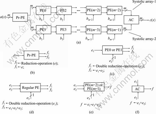
Fig. 4 Proposed low latency systolic structure: (a) Systolic structure; (b) Function of Pr-PE; (c) Function of PE0 or PE1; (d) Function of regular PE; (e) Function of PE(m-2) or PE(m-1); (f) Function of AC
The circuit designs of the PEs are shown in Fig. 5. The Pr-PE contains a degree-reduction cell (DRC), which corresponds to the cell R of the SFG in Fig. 2. The detail of the PE0 or PE1 is a little more complex than the Pr-PE, where it contains two DRCs and an AND cell. The AND cell corresponds to the cell A of SFG in Fig. 2. A regular PE may contain two DRCs, an AND cell and a XOR cell. The XOR cell corresponds to the cell M of SFG in Fig. 2. The PE(m-2) or PE(m-1) contains an AND cell and a XOR cell, and there is no DRC in the PE. The AC only needs a XOR cell since it only performs the addition operation. Note that the AND cell and XOR cell contain m number of logic gates working in parallel, and
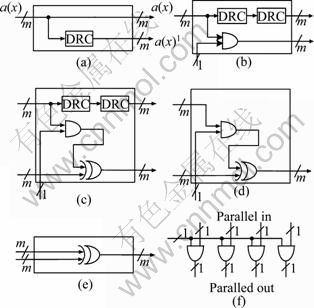
Fig. 5 Circuit designs of PEs: (a) Circuit design of Pr-PE; (b) Circuit design of PE0 or PE1; (c) Circuit design of regular PE; (d) Circuit design of PE(m-2) or PE(m-1); (e) Circuit design of AC; (f) An example of AND cell (m=4)
Fig. 5(f) gives an example of such design, where m=4. To a regular PE, the bits of reduced form operand a(x)j from its left are fed to the AND cell in parallel, and another input of the AND cell is connected to one bit of operand b(x), during each cycle period. The output of the AND cell is fed to one input of the XOR cell, and another input from left of the PE is fed to another input of the XOR cell. Meanwhile, the input operand a(x)j from left is also fed to the two DRCs. At last, the outputs of the DRC and the XOR are latched out to the next PE on its right. The operation happening in DRC can be achieved by t number of XOR gates, according to Refs. [11] and [12].
Note that according to Refs. [11] and [12], the time required by a cell R will be TX. Therefore, two DRCs may require a delay time of 2TX. The duration of minimum cycle period of a PE amounts to max{2TX, (TA+TX)}=2TX. The proposed low latency systolic design yields the first output of desired product (m/2)+2 cycles after the first input is fed to the structure, while the successive outputs are available in each cycle.
It is observed that the PEs in the two systolic arrays in Fig. 4 have some identical circuit-cells. Taking the PE0 and PE1 as an example, as shown in Fig. 6, it can be seen that the output of the DRC2 in PE0 is a(x)2, while the output of DRC3 in PE1 is also a(x)2. This makes it possible that the output of the DRC3 of PE1 can be shared if we combine the PE0 and PE1 together into one PE, and Fig. 7 shows such design. It can be seen that the DRC1 and DRC2 in the former PE0 have been moved, which means the XOR gates required by the DRC1 and DRC2 have been saved. Similarly, we can combine the PE2 and PE3 in Fig. 4 into a new PE. And likewise, each PE of systolic array-1 and the corresponding PE of systolic array-2 in Fig. 4 can be combined together into a new PE. Figure 8 shows the proposed low latency structure after the PEs have been redesigned, where the whole structure consists of (m+1) PEs, i.e., one Pr-PE and m new PEs. Note that the PE{1} corresponds to the PE0 and PE1 in the structure in Fig. 4, the PE{2} corresponds to the PE2 and PE3 in the structure in Fig. 4, and so on. The circuit design of each PE is similar to that of Fig. 7. Therefore, m DRCs in the former structure have been saved, and consequently, the XOR gates required by the m DRCs have been saved. Note that the critical path of a PE and the latency of the structure are the same as those in Fig. 4.
2.3 Proposed design for pentanomials
Let f(x) be a pentanomial in the form of
 (14)
(14)
where 1= k123 Comparing Eq. (14) with Eq. (1), one can find some (fi) are “0”, and some (fi) are “1”. Therefore, the systolic structure proposed in subsection A can also be used for multiplication over GF(2m) based on pentanomials. Since the two structures are similar, here the design of the structure is skipped. But a digit-level low latency systolic structure is obtained.

Fig. 6 Circuit designs of PE0 (a) and PE1 (b)

Fig. 7 Circuit design of new PE
Note that the neighboring two PEs in Fig. 8 can be implemented by one PE, such that the bits of the operand b(x) are fed to PE in a digit-level way. For example, the PE{1} and PE{2} in Fig. 8 can be implemented by one PE, as shown in Fig. 9, where the digit-level w=2. Similarly, (m/2) PEs of structure in Fig. 8 can be implemented by (m/4) PEs, where each of the digit-level PEs is similar to that in Fig. 9. Therefore, the digit-level structure will have a latency of (m/4)+2 cycles, and the minimum duration of a cycle period of a PE will be 4TX, since there are four DRCs in a PE. The time complexity is nearly the same as that in Fig. 8, but the registers required for the structure have been reduced to half.

Fig. 8 Proposed low latency systolic structure

Fig. 9 Circuit design of digit-level PE
Note that the digit-level w can be a large number, so that the registers will be reduced significantly. For example, if we assume w=4, then the registers requirement will be reduced to only 25% of that in Fig. 8. Meanwhile, the time complexity nearly does not change.
3 Hardware and time complexity
3.1 Complexity of structure for general irreducible polynomials
When using the structure in Fig. 8 on efficient realization of the multiplication over GF(2m) based on general irreducible polynomials, the whole structure will require (m/2+1) PEs and an AC. According to Eqs. (11) and (12), each DRC in the PE would require t XOR gates. Therefore, the whole structure will require m2 AND gates and (m2+m・t-m) XOR gates. Besides, 2m2 registers are required for the PEs. The duration of minimum cycle period of a PE amounts to 2TX. The latency of the proposed systolic design is (m/2)+2 cycles. The gate-counts, register-counts, latency and critical path of the proposed structure and the existing systolic structure of Ref. [16] for multiplication over GF(2m) based on general irreducible polynomials are listed in Table 1. Note that we also list the area time complexity of the digit level low latency systolic structure where w=2.
3.2 Complexity of structure for general irreducible pentanomials
When using the structure in Fig. 8 on efficient realization of the multiplication over GF(2m) based on pentanomials, the whole structure will require (m/2+1) PEs and an AC. According to Eqs. (11) and (14), each DRC in the PE would require three XOR gates. Therefore, the whole structure will require m2 AND gates and (m2+2m) XOR gates. Besides, 2m2 registers are required for the PEs. The duration of minimum cycle period of a PE amounts to 2TX. The latency of the proposed systolic design is (m/2)+2 cycles. The gate-counts, register- counts, latency and critical path of the proposed structure and the existing systolic structure of Ref. [13] for multiplication over GF(2m) based on pentanomials are listed in Table 1. Also, the complexity of the digit level low latency systolic structure is listed where w=2.
3.3 Comparison and discussion
Note that in Ref. [17], it was suggested to use the NAND gate to replace the AND gate in the PE to obtain a low critical path design. Since most of the other existing designs use the AND gate, here the AND gate is used for replacing the NAND gate, although it is easy to use the NAND gate to replace the AND gate in the PE, just for a fair comparison.
It can be seen that the proposed designs outperform the corresponding existing systolic designs [16]. For the proposed design for polynomial basis multiplier, when compared with the systolic design in Ref. [16], the proposed design involves nearly the same hardware requirement as that of the design in Ref. [16]. But the latency of the proposed design is reduced to half. Besides, the critical path of the proposed design is shorter than that of Ref. [16]. Moreover, the proposed digit-level structure again reduces the register requirement to half while the time complexity nearly does not change.
Table 1 Hardware- and time-complexity of proposed systolic structures and existing systolic structures for finite field multiplication over GF(2m) based on general irreducible polynomial and pentanomial

For the proposed design for pentanomial basis multiplier, when compared with the systolic design in Ref. [17], the proposed design involves nearly the same hardware requirement as that of the design in Ref. [17]. But the latency of the proposed design is reduced to half. And the time complexity of the proposed design is nearly m・TX, while the time complexity of the existing design [17] is m・(TA+TX). It is clear that the proposed low latency pentanomial basis systolic multiplier involves nearly one-third less area-delay product compared with the existing design. Besides, the proposed digit-level structure again reduces the register requirement to half while the time complexity nearly does not change.
To estimate the performance of the proposed design, f(x)=x163+x7+x6+x3+1 is used as example. Also the area-time complexity of the proposed design is obtained from TSMC 0.18 μm process 1.8 V SAGE-X standard cell library data-book. The area of the proposed design is 4 074 114 μm2, and the critical path of the design is 0.4 ns.
4 Conclusions
1) Two efficient low latency systolic structures are presented for polynomial basis multiplication over GF(2m) based on general irreducible polynomials and pentanomials, respectively. First of all, two low latency systolic structures are presented for multiplications over GF(2m) based on general irreducible polynomials and pentanomials from the SFG by suitable cut-set retiming. To reduce the hardware requirement further, two digit-level systolic structures are also presented.
2) Interestingly, the two structures both reduce the latency to nearly (m/2) cycles with a minimum duration of critical path of (2TX), while on the other side, the hardware requirements of the two systolic designs do not increase. It is found that the proposed three low latency designs are efficient in area-time complexity when compared with the existing designs. The digit-level systolic structures can reduce the register requirement to half but their time complexities do not change.
3) To the authors’ knowledge, the time-complexity of the structures are the lowest found in literature for systolic GF(2m) multipliers based on general irreducible polynomials and pentanomials. Because of their efficiency in area-time complexity, accordingly, the proposed low latency designs can be applied in a lot of environments.
References
[1] Deschamps J P, Imana J L, Sutter G D. Hardware implementation of finite field arithmetic [M]. New York: McGraw-Hill, 2009: 45-49.
[2] Blake I, Seroussi G, Smart N P. Elliptic curves in cryptography, ser [M]. London Mathematical Society Lecture Note Series Cambridge, UK: Cambridge Univ Press, 1999: 75-78.
[3] Chen S H, Yan H Z, Ming X Z. Analysis and modeling of error of spiral bevel gear grinder based on multi-body system theory [J]. Journal of Central South University of Technology, 2008, 15(5): 706-711.
[4] Jiang A H, Mei C, E J Q. Nonlinear combined forecasting model based on fuzzy adaptive variable weight and its application [J]. Journal of Central South University of Technology, 2010, 17(4): 863-867.
[5] LEE S H, WANG Y Q, SONG J I. Fourier and wavelet transformations application to fault diction of induction motor with stator current [J]. Journal of Central South University of Technology, 2010, 17(1): 93-101.
[6] WU J S, SHU H Z, WANG L, SENHADJI L. Fast algorithms for the computation of sliding sequency-ordered complex hadamard transform [J]. IEEE Trans Signal Process, 2010, 58(11): 5901-5909.
[7] Yeh C S, Reed I S, Truong T K. Systolic multipliers for finite fields GF(2m) [J]. IEEE Trans. Computers, 1984, 33(4): 357-360.
[8] Wang C L, Lin J L. Systolic array implementation of multipliers for finite fields GF(2m) [J]. IEEE Trans Circuits Syst, 1991, 38(7): 796-800.
[9] Sunar B, Koc C K. Mastrovito multiplier for all trinomials[J] IEEE Trans Comput, 1999, 48(5): 522-527.
[10] Song L, Parhi K K, Kuroda I, Nishitani T. Hardware/software code sign of finite field data path for low-energy Reed-Solomn codes [J]. IEEE Trans Very Large Scale Integr (VLSI) Syst, 2000, 8(2): 160-172.
[11] Lee C Y, Lu E H, Lee J Y. Bit-parallel systolic multipliers for GF(2m) fields defined by all-one and equally spaced polynomials [J]. IEEE Trans Comput, 2001, 50(6): 385-393.
[12] Lee C Y. Low complexity bit-parallel systolic multiplier over GF(2m) using irreducible trinomials [J]. IEE Proc Comput Digit Tech, 2003, 150(1): 39-42.
[13] Lee C Y, Chiou C W, Lin J M, Chang C C. Scalable and systolic Montgomery multiplier over GF(2m) generated by trinomials [J]. IET Circuits Devices Syst, 2007, 1(6): 477-484.
[14] Lee C Y, Horng J S, Jou I C, Lu E H. Low-complexity bit-parallel systolic Montgomery multipliers for special classes of GF(2m) [J]. IEEE Trans Comput, 2005, 54(9): 1061-1070.
[15] Jain S K, Song L, Parhi K K. Efficient semisystolic architectures for finite field arithmetic [J]. IEEE Trans Very Large Scale Integr (VLSI) Syst, 1998, 6(1): 734-749.
[16] Sarmadi S B, Hasan Anwar M. Concurrent error detection in finite-field arithmetic operations using pipelined and systolic architectures [J]. IEEE Trans Comput, 2009, 58(11): 1553-1567.
[17] Meher P K. Systolic and non-systolic scalable modular designs of finite field multipliers for Reed-Solomon codes [J]. IEEE Trans Very Large Scale Integr (VLSI) Syst, 2009, 17(6): 747-757.
[18] MAO Z, SHOU G, HU Y, GUO Z. Design of multipliers for GF(2m) [J]. Electron Lett, 2010, 46(6): 419-420.
[19] FAN H N, HASAN M A. Alternative to the Karatsuba algorithm for software implementations of GF(2n) multiplications [J]. IET Information Security, 2009, 3(2): 60-65.
[20] Parhi K K, VLSI digital signal processing systems: Design and implementation [M]. New York: Wiley, 1999: 189-223.
(Edited by YANG Bing)
Foundation item: Project(61174132) supported by the National Natural Science Foundation of China; Project(09JJ6098) supported by the Natural Science Foundation of Hunan Province, China
Received date: 2011-02-28; Accepted date: 2011-08-02
Corresponding author: HE Jian-jun, Professor, PhD; Tel: +86-13507465056; E-mail: jjhe@csu.edu.cn

