2.7-4.0 GHz PLL with dual-mode auto frequency calibration for navigation system on chip
��Դ�ڿ������ϴ�ѧѧ��(Ӣ�İ�)2016���9��
�������ߣ���־�� ���� ��С�� ���
����ҳ�룺2242 - 2253
Key words��auto frequency calibration; phase lock loop; voltage control oscillator; lock time
Abstract: A 2.7-4.0 GHz dual-mode auto frequency calibration (AFC) fast locking PLL was designed for navigation system on chip (SoC). The SoC was composed of one radio frequency (RF) receiver, one baseband and several system control parts. In the proposed AFC block, both analog and digital modes were designed to complete the AFC process. In analog mode, the analog part sampled and detected the charge pump output tuning voltage, which would give the indicator to digital part to adjust the voltage control oscillator (VCO) capacitor bank. In digital mode, the digital part counted the phase lock loop (PLL) divided clock to judge whether VCO frequency was fast or slow. The analog and digital modes completed the auto frequency calibration function independently by internal switch. By designing a special switching algorithm, the switch of the digital and analog mode could be realized anytime during the lock and unlock detecting process for faster and more stable locking. This chip is fabricated in 0.13 ��m RF complementary metal oxide semiconductor (CMOS) process, and the VCO supports the frequency range from 2.7 to 4.0 GHz. Tested 3.96 GHz frequency phase noise is -90 dBc/Hz@100 kHz frequency offset and -120 dBc/Hz@1 MHz frequency offset. By using the analog mode in lock detection and digital mode in unlock detection, tested AFC time is less than 9 ��s and the total PLL lock time is less than 19 ��s. The SoC acquisition and tracking sensitivity are about -142 dBm and -155 dBm, respectively. The area of the proposed PLL is 0.35 mm2 and the total SoC area is about 9.6 mm2.
J. Cent. South Univ. (2016) 23: 2242-2253
DOI: 10.1007/s11771-016-3282-y

CHEN Zhi-jian(��־��), CAI Min(����), HE Xiao-yong(��С��), XU Ken(���)
School of Electronic and Information Engineering, South China University of Technology, Guangzhou 510640, China
 Central South University Press and Springer-Verlag Berlin Heidelberg 2016
Abstract: A 2.7-4.0 GHz dual-mode auto frequency calibration (AFC) fast locking PLL was designed for navigation system on chip (SoC). The SoC was composed of one radio frequency (RF) receiver, one baseband and several system control parts. In the proposed AFC block, both analog and digital modes were designed to complete the AFC process. In analog mode, the analog part sampled and detected the charge pump output tuning voltage, which would give the indicator to digital part to adjust the voltage control oscillator (VCO) capacitor bank. In digital mode, the digital part counted the phase lock loop (PLL) divided clock to judge whether VCO frequency was fast or slow. The analog and digital modes completed the auto frequency calibration function independently by internal switch. By designing a special switching algorithm, the switch of the digital and analog mode could be realized anytime during the lock and unlock detecting process for faster and more stable locking. This chip is fabricated in 0.13 ��m RF complementary metal oxide semiconductor (CMOS) process, and the VCO supports the frequency range from 2.7 to 4.0 GHz. Tested 3.96 GHz frequency phase noise is -90 dBc/Hz@100 kHz frequency offset and -120 dBc/Hz@1 MHz frequency offset. By using the analog mode in lock detection and digital mode in unlock detection, tested AFC time is less than 9 ��s and the total PLL lock time is less than 19 ��s. The SoC acquisition and tracking sensitivity are about -142 dBm and -155 dBm, respectively. The area of the proposed PLL is 0.35 mm2 and the total SoC area is about 9.6 mm2.
Key words: auto frequency calibration; phase lock loop; voltage control oscillator; lock time
1 Introduction
There is stronger demand on wireless and handheld navigation application receivers to get position information never before expected and in times [1]. The radio frequency (RF) phase lock loop (PLL) is the ��slowest�� block in receiver because the lock time of the PLL often takes hundreds of microseconds or even longer. Recently RF PLL is becoming the most important module in modern communication system because of the tight frequency allocation. Due to the high performance of the PLL, wide voltage control oscillator (VCO) tuning range, fast lock time and low phase noise become the key features in recent wireless communication or navigation circuit design [2]. The satellites are about 12000 km far from us, so the satellite signal strength at the antenna is below thermal noise floor [3]. A high performance PLL is needed to transfer the weak RF signal to baseband. Due to the foundry process, voltage and the temperature (PVT) variations, it is very common that the VCO free-run frequency will change more than ��30% in fabrication. Thus, a wide VCO tuning range and fast PLL lock time are important for navigation system on chip (SoC).
The wide VCO tuning range is usually achieved by using an LC VCO which has a switch capacitor bank [4]. To keep the phase noise low, the VCO has multiple sub-band tuning curves that can decrease the KVCO (VCO gain). The VCO frequency calibration principle is to find the correct sub-band tuning curve for a target frequency before the PLL fine locking begins. There are many methods available in public literatures [5-7] so far. However, they all showed some drawbacks. Their schemes are detecting the frequency error between reference clock and the divided clock in digital method [8] or detecting the tuning voltage by using large charge pump current before PLL lock, which brings a fast charge, discharge current and wide loop bandwidth in analog mode [9]. However, they are single mode only. Digital mode takes long time to count the clock to meet the AFC accuracy due to the slow clock-counting and is also with complicated logic computing. Analog mode with the feature of simple structure showed a faster calibration, but it is more prone to be out of work due to the unstable state and large bandwidth.Therefore, in this work, we present a dual-mode method for VCO auto frequency calibration. This method mainly combines the digital with analog mode for auto frequency calibration. By using the analog mode in lock detecting state and digital mode in unlock detecting state, the PLL will get a faster and more accurate search in frequency calibration process than the conventional single mode calibration methods. By designing a special switch algorithm, the switch of the digital and analog mode can be realized anytime during the lock and unlock detecting process for faster and more stable locking.
2 SoC architecture
The navigation applications inside numerous handheld electronic devices, such as cell phones and PADs, demand the navigation system to have low power consumption, small package and high performance [10]. For low noise requirement, conventional navigation solution often adapts two RF surface acoustic wave (SAW) filters before and after an external low noise amplifier (LNA) [11]. However, it is highly desirable to eliminate the external LNA and the SAW filter due to cost of bill of material (BOM) [12], which demands a great design challenge to integrate RF, baseband and other function building blocks on a single chip with very low power consumption. To achieve these requirements, a more complicated SoC is needed to fulfil the whole function and performance of navigation.
Figure 1 shows the overall architecture of the navigation SoC including an RF receiver, a baseband processor and other system control parts as power manage unit (PMU), real time clock (RTC) and etc. For faster computing speed, the SoC embedded digital signal processing (DSP) with 4-kbyte program memory (PM) words and 4-kbyte data memory (DM) words and provides universal asynchronous receiver/transmitter (UART) interface with duplex modes. The availability of an embedded 4-kbyte memory allows the storing of navigation information to optimize start-up performances. By using DMA interface, the system hardware can transfer the data without software. The SoC can acquire a satellite with strong signal in 3 ms@85 MHz and acquires 32 satellites in sequence by default (from satellite 1 to satellite 32), otherwise in software configuration sequence.
The proposed RF receiver architecture is depicted in Fig. 2. The RF receiver is a low intermediate frequency (IF) receiver [13] which provides the complete antenna-to-baseband transfer for the SoC. Eliminating the IF SAW filter and the external LO generation [14-15], the RF block integrates all the modules including low noise amplifier (LNA), mixer, IF filter, auto gain control (AGC) amplifier and analog-to-digital converter (ADC). Also the VCO [16], PLL, loop filter and calibration circuits are fully integrated on chip which dramatically reduces the number of external components. Only an antenna, a crystal, and few passive devices for input match are required to complete the application. The radio signal that received by antenna is amplified by LNA and then converted to the 4.092 MHz IF [17] by the mixer after which, the IF signal is filtered by band-pass filter and amplified by AGC amplifier to a fixed amplitude due to the ADC dynamic range limit. ADCs convert the amplified IF signal to digital and send them to baseband block for position and time computing and locating.
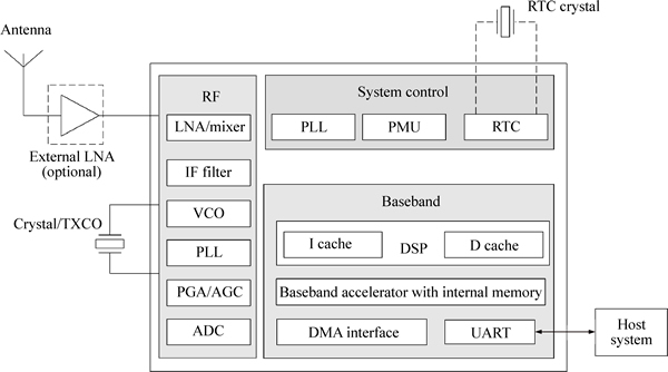
Fig. 1 Structure diagram of navigation SoC
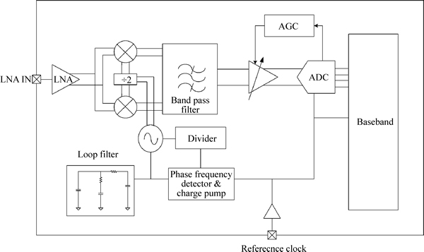
Fig. 2 Block diagram of navigation receiver
3 Design of RF PLL and auto frequency calibration
3.1 RF PLL structure
RF PLL is the essential component in many applications including navigation receivers. The most important characteristics of high-performance PLLs are low phase noise and fast lock time. The diagram of the RF PLL structure, as illustrated in Fig. 3, consists of an auto frequency calibration (AFC) [18] part and a PLL part. The PLL is partitioned into phase frequency detector (PFD), charge pump, three-order loop filter, VCO with switch capacitor bank and dividers. To generate the quadrature local oscillator (LO) signal for mixer in receiver path, the VCO frequency is running at about 2.7-4.0 GHz. After divided by 2, the LO signal is sent to mixer, and simultaneously feeds the divider module to get the comparing clock for PFD. PFD detects the frequency and phase error between the reference and the divided clock then makes the charge pump to charge or discharge the loop filter till the PLL is locked. A 16.368 MHz reference clock for the PLL and a loop bandwidth of 100 kHz is chosen for phase noise optimization.
The proposed AFC block consists of the state machines of the digital and analog mode, the binary searching logic, the frequency decide logic and analog circuits for analog mode. When the chip is powered on, the whole PLL is reset and AFC begins to work. Either analog or digital mode is chosen, AFC will make a decision to tune the capacitor bank according to that whether VCO is too fast or too slow. When the correct sub-band tuning curve for a target frequency is found, the PLL fine locking will begin till PLL is locked. And after lock detecting process, AFC enters the unlock-detecting state. In the unlock-detecting state, AFC process will restart when the PLL is unlock.
3.2 Design of phase frequency detector & charge pump
The non-ideal effects of the PLL will introduce the reference spur in spectrum. The delay offset in phase frequency detector (PFD), charge pump (CP) leakage current and the mismatch are the most important issues in PLL design to reduce the reference spur level. The reference spur (Pspur, dBc) due to the non-ideal effects in PFD and CP is approximately given by [19]
 (1)
(1)
where fBW is the PLL loop bandwidth, �� is the phase errors in PFD and CP, N is the PLL division ratio, and fp1 is the pole of the loop filter.
The phase error (��, rad) due to the CP leakage current is given by
 (2)
(2)
Assuming fBW=100 kHz, fref=16 MHz, fout=3.2 GHz (N=200), fp1=400 kHz, ICP=1 mA, and Ileakage=100 nA, then the reference spur due to the CP leakage current Pspur=-113 dBc.
The reference spur due to the timing mismatch in PFD is approximately given by [19]
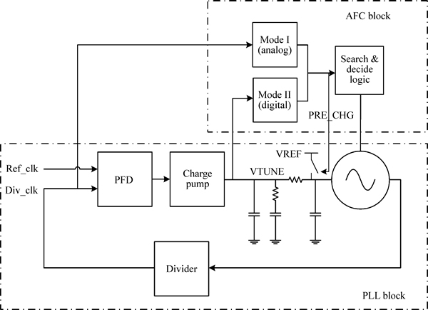
Fig. 3 Block diagram of PLL and AFC
 (3)
(3)
where ��ton and ��td are the turn on time and delay mismatch of the PFD.
By using the same condition for Eq. (1) and assuming ��ton=1 ns and ��td=5 ps, the reference spur due to the timing mismatch in PFD Pspur=-119 dBc.
The reference spur due to the mismatch in CP is approximately given by [19]
 (4)
(4)
where ��i is the current mismatch in CP.
Assuming ��ton=1 ns and ��i=10 ��A, the reference spur due to the mismatch in CP Pspur=-93 dBc.
These equations show that it is important to consider the PFD/CP with the minimum leakage current, turn on time and the mismatches. And an optimized loop bandwidth and CP current is also important to reduce the spurs. In PLL, the dominant factor that determines the level of the reference spur mismatches CP. Therefore, the proposed PFD and CP are well-designed to minimize the mismatch from the current and delay.
The PFD [20] circuit includes 2 D Flip-Flops,2 MUXs, 1 NOR, some transmission gates and inverters for generating equivalent differential delay output UP, UP_B, DN and DN_B signals. When REF_CLK's frequency or phase leads DIV_CLK��s, PFD outputs is ��1�� pulse at UP port. When REF_CLK��s frequency or phase lags DIV_CLK��s, PFD outputs is ��1�� pulse at DN port and conversely for other two states. REF_CLK and DIV_CLK can be cross switched by MUX��s control bit for testing. For eliminating the dead zone problem tunable capacitors are designed to turn on the CP in 0.7-2.1 ns.
As shown in Fig. 4, the CP is composed of BIAS circuits, error feedback circuits, bias replica circuits and switching core circuits. The MOSFETs of the CP current sources are carefully designed and laid out to minimize mismatches especially for eliminating the mismatch between ��UP�� and ��DN" current. As well as cascode and differential structure are adopted for the current source to decrease the mismatch. The differential outputs of the CP (points A and B) are connected by a negative error feedback loop using a unit-gain-amplifier. Therefore, the charge sharing problem [21] is effectively reduced by this. Another replica bias loop [22] technique is adopted to make points A, B and C at the same common voltage. Adjusting the bias current and the CP current to make ��UP�� and ��DN�� current equal can reduce the mismatch between the current sources. The dummy MOSFETs added between the UP/DN switch core and the current switching MOSFETs are able to effectively suppress the output ICP current peaking caused by possible timing mismatches between the UP/DN pulses.
3.3 Design of LC-VCO
The LC-VCO usually adopts Colpitts oscillator structure for low noise design [23]. However, compared to negative resistance oscillators, power consumption is the drawback for Colpitts oscillator. Moreover, stacking MOS transistors can hardly be used in VCO design in 0.13 ��m CMOS technology due to the voltage headroom limitation.
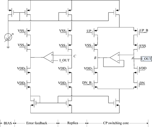
Fig. 4 Block diagram of charge pump
As shown in Fig. 5, the VCO employs cross- coupled NMOS differential transistor pairs (M1 and M2) to generate the negative resistance. In RF domain, NMOS performance is much better than PMOS, therefore the NMOS cross-coupled transistor pairs are often used in RF VCO design. The inductor, the coarse- tuning capacitor bank and the fine-tuning varactors form the tank load of the cross-coupled transistor pairs. For getting a better tradeoff between power and phase noise, the bias of VCO is adjustable through register control. The tail resistor (Rt) instead of a tail current source is adopted for suppressing 1/f noise.
Due to the low frequency noise up-conversion, the phase noise is in proportion to KVCO. For low phase noise, it is desirable to have KVCO as small as possible, but small KVCO means narrow frequency locking range [16]. To decrease the noise (or KVCO), the proposed VCO adopts a binary-weighted 6 bits coarse tuning switched capacitor bank which has 64 capacitor values. The frequency of the LC-VCO is given by
 (5)
(5)
where Cvar, Cbank and Cpar are the capacitances of the varactor, switch capacitor bank and the parasitic capacitors, respectively.
The structure of the capacitor bank cell unit is shown in Fig. 5. Therefore, the KVCO is significantly reduced by this. In this design, NMOS transistors are used to design the RF switches. The Q factor of the capacitor cell is written as [24]
 (6)
(6)
where CS is the total tank resonator capacitor, and the turn on resistor (Ron) is given by
 (7)
(7)
where ��n is the electrons mobility, and Cox is the MOS gate capacitor.
Therefore, a single NMOS switch M5 for two capacitors in differential is used, which has a large size and small Ron for good phase noise and will improve the Q factor of the capacitor bank. M3 and M4 provide a bias voltage to avoid a floating state for capacitor and an even smaller resistance when M5 is on. Moreover, using NMOS as resistor will reduce the area of the cell.
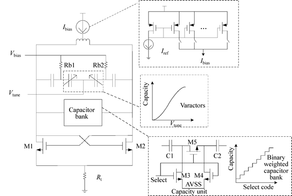
Fig. 5 Structure of VCO
Because of the PVT variations, it is very common that the VCO free-run frequency will change more than ��30% in fabrication. Therefore, switch capacitor bank that would cover the range of more than 1 GHz must be well designed for the VCO. According to Eq. (5), the unit capacitor is given by
 (8)
(8)
where Cmin is the minimum capacitor of the tank load, fvco is the target VCO frequency and fvar is the varactor tuning range at the highest KVCO. For the proposed LC-VCO, fvco of 4 GHz, Ltank of 1.5 nH, Kvco of 77 MHz/V, Vtune range of 0.6 V, the capacitor unit of the proposed VCO can be estimated to be 34 fF using metal-insulator-metal (MIM) unit capacitors, which is verified through following simulations.
3.4 Design of auto frequency calibration
The proposed AFC structure is shown in Fig. 6 and its flowchart is shown in Fig. 7. After AFC calibration starts, the digital block is reset and the Vtune voltage is pre-charged to half power supply. The capacitor bank selected code is set to 100000. AFC can run in two modes, analog and digital one. Both of them adopt binary searching algorithm and start from the most significant bit (MSB) of the selected code.
In analog mode, a large ICP current is chosen before calibration decision, which allows a faster charge or discharge and a wider PLL loop bandwidth for speeding the calibration. The AFC part samples and detects the charge pump output Vtune voltage and give an indicator (lock_det_ana<1:0>) to digital part (lock/unlock detector). When the charge pump output Vtune voltage increases to a high threshold (Vhigh), it shows that the VCO frequency is lower than expectation. The VCO frequency should be turned high and decide logic will give out lock_det_ana<1:0>=01. The digital logic part will decrease the capacitors in the VCO capacitor bank. Conversely, when the charge pump output Vtune voltage decreases to a low threshold (Vlow), it shows that the VCO frequency is higher than expectation. The VCO frequency should be turned low and decide logic will give out lock_det_ana<1:0>=10. The digital logic part increases the capacitors in the VCO capacitor bank. When the voltage is between Vhigh and Vlow for a period of time, it shows that the VCO is running at the expectable frequency range, the capacitor bank will be at the correct value and decide logic will give out lock_det_ana<1:0>=00, then AFC lock detecting is done.
Charge pump current (ICP) and the loop filter parameters dominate the AFC time of the analog mode. As shown in Fig. 8, the transfer function of the 3rd order loop filter is as below
 (9)
(9)

Fig. 6 Block and algorithm of AFC
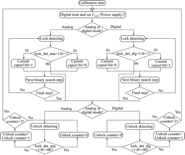
Fig. 7 Flowchart of AFC
where ��2=R2C2, ��3=R3C3 and Ctotal=C1+ C2+C3.
The transfer function of the PLL loop is as below:
 (10)
(10)
where �� is the ratio of the ��on�� period of the CP switches to a reference clock period. Hence, the unit step input response of Vtune(s) can be expressed as
 (11)
(11)
By inverse Laplace transforming Vtune(s), we get the time domain function of Vtune(t):


 (12)
(12)
where  B and C are the coefficients, and since ��1>>t, ��3>>t, C2>>C1, C2>>C3 and Vtune is equal to VDD/2 at the initial time of AFC, the analog AFC time for one step can be simplified as
 (13)
(13)
The AFC time of the proposed PLL can be estimated from Eqs. (11) and (13), since the zero and the poles from C1, C2 and R2 in Fig. 8 are dominant. For the proposed PLL, 6 bit VCO switches, Icp (at AFC state) of 15 mA, C2 of 100 pF, Vlow of 0.3 V and Vhigh of 0.9 V are utilized. Therefore, the worst-case of the proposed PLL can be estimated to be 8 ��s, which is also verified through following simulations.
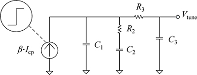
Fig. 8 3rd loop filter for PLL
In digital mode, the PLL divided clock (clk_div) feeds the frequency decider block to determine the VCO frequency. The frequency decider counts the PLL divided clock by using the reference clock. The countable time of the divided clock should be designed carefully for the AFC coarse tuning, which should cover the fine tuning range.
The AFC coarse tuning accuracy AAFC is decided by the following:
 (14)
(14)
where Kvco is the VCO gain, ��V is the varactor tuning range, fvco and fref are the VCO and reference clock frequency, and N is the PLL��s total division ratio. In this design, for example, the minimum and maximum Kvco@VDD/2 are about 37 and 77 MHz/V and the tuning range of the varactor is about 600 mV. The PLL��s total division ratio is about 192 by using a 16.368 MHz reference. So the accuracy of the AFC is about 1.6%, which means the time of AFC should be more than 64 reference clocks to guarantee that accuracy.
When counting 64 reference clock for example, if divided clock is <64, it shows that the VCO frequency is lower than expectation, the VCO frequency should be turned high and decide logic will give out lock_det_dig<1:0>=01. If divided clock is higher than 64, it shows that the VCO frequency is higher than expectation and the VCO frequency should be turned low and decide logic will give out lock_det_ dig<1:0>=10. When the divided clock=64, it shows that the VCO is running at the expectable frequency range and the capacitor bank is also at correct value and decide logic will give out lock_det_dig<1:0>=00, the AFC is done.
After lock detecting process, AFC enters the unlock-detecting state. When detecting three times continuous unlocking, AFC will restart the AFC process. The analog and digital mode of the AFC can complete the auto frequency calibration function independently by internal switch. The output logic detected their results and gave out the PLL lock signals. By designing a special switch arithmetic, the switch of the digital and analog mode can be realized anytime during the lock and unlock detecting process for faster and more stable locking.
4 Simulation and experimental results
Figures 9 and 10 show the simulation results of the PLL AFC. In digital mode, AFC time can be adjusted by registers for calibration. The results show that the PLL AFC circuits automatically start to tune the VCO capacitor bank to a correct value. The AFC finished t whole frequency calibration in about 25 ��s through 6 steps, and every step is about 4 ��s. The capacitor bank starts from ��100000��, then the change steps are ��100000��010000��001000��001100��001010��001011��001100��. After the AFC calibration is done, the digital logic sends out ��afc_done=1�� signal. Then the PLL fine tuning circuits begin to work till the PLL is locked at 24.7 ��s.
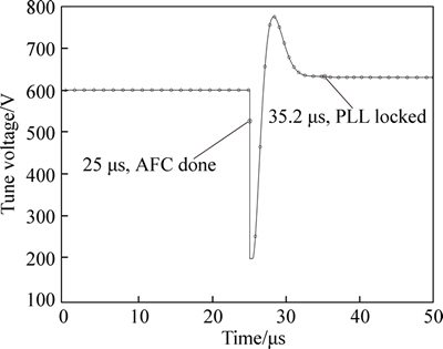
Fig. 9 Simulation results of AFC-Vtune voltage
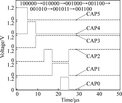
Fig. 10 Simulation results of AFC-Capacitor bank code
Figure 11 shows a test PCB and a die microphotograph of the navigation SoC. The total chip area is about 9.6 mm2 and packaged in a 40-pin QFN package. The PLL active area is 0.35 mm2 and all of the building blocks are encircled by double guarding-ring to minimize noise such as digital and substrate noise fromDSP and processor. The PLL total power consumption is 7 mA including the power consumption of the AFC circuit.
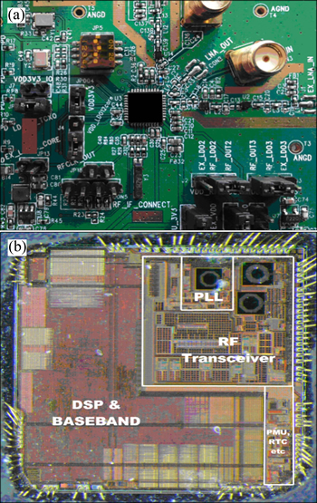
Fig. 11 Photos of test PCB (a) and die microphotograph of SoC (b)
Figure 12 shows the VCO frequency tuning curves versus the Vtune voltage. The VCO switch capacitors bank is binary weighted and controlled by 6 bits for a total 64 curves. Figure 13 shows the VCO gain (Kvco) versus the vtune voltage. The gain curves show large variations across the vtune voltage and the most variation is at the highest frequency (cap bank code=000000). It is caused by most of the capacitive devices of the tank, which is made up of varactors in that condition. The region of greatest linearity and peak gain occurs around at common voltage is a result of accumulation-mode MOS varactors in deep-submicron CMOS processes, as measurements in Ref. [19] also confirms. This makes them ideal for work in tuning VCO where large headroom can be achieved by setting the common-mode value of the control voltage to half the supply and limiting their operation region as just described. Therefore, the AFC is used to maintain work at the voltage about 600 mV (in the middle of VDD). This reduces the gain variation to acceptable levels for AFC function.
The VCO and PLL phase noise and output spectrum are measured by Agilent power spectrum analyzer E4440A and signal source analyzer E5052B. The reference spur is -61 dBc which exactly appears at the reference frequency of 16 MHz. Due to the substrate coupling, VDD/GND interference, the reference spur is a little bigger than which is computed above. VCO output power is about -0.8 dBm which is equal to 580 mV (peak to peak) at 50 �� impedance and is enough to drive next block. Figure 14 shows the phase noise when the VCO frequency is tuned to 3.96 GHz. The measured phase noise at 100 kHz offset is -90 dBc/Hz and the out-band phase noise is -120 dBc/Hz at 1 MHz offset.
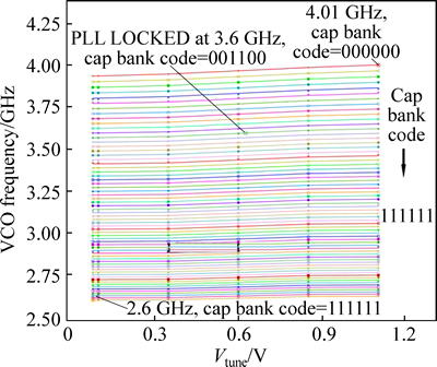
Fig. 12 VCO tuning characteristics��outpu t frequency range
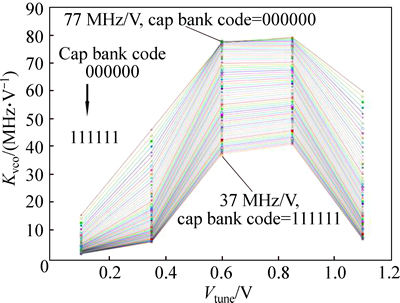
Fig. 13 VCO tuning characteristics��VCO gain (Kvco)
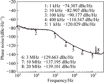
Fig. 14 Measured phase noise of PLL at 3.96 GHz
The PLL lock time and AFC calibration test results are shown in Fig. 15. By using the analog mode in locking detecting state for fast locking and digital mode in unlock detecting state for more stable, it shows that when the PLL is power on, the AFC circuits automatically start to tune the VCO capacitor bank to a correct value according to the charge pump output voltage by using analog AFC mode. After 9 ��s the AFC calibration is done and the PLL entered the fine tuning step till the PLL is locked. According to the result, the PLL locked in is about 19 ��s. After that the digital mode is adopted to ensure that the PLL is lock. When the PLL is not locked and the digital unlock detecting mode will restart the AFC process. The total AFC time is less than 9 ��s and the total PLL lock time including the AFC time is less than 19 ��s. Table 1 summarizes the performance of the proposed PLL design.
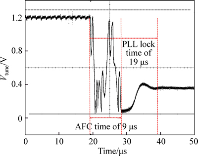
Fig. 15 Measured PLL locking wave
Table 1 PLL performance summary

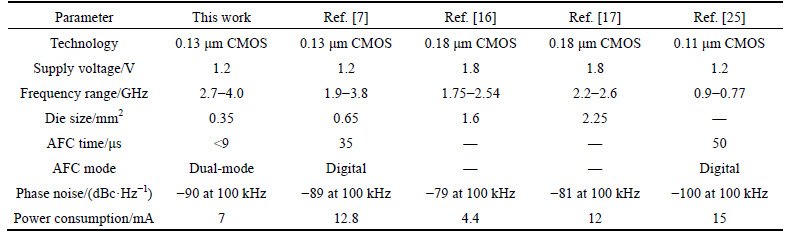
Table 2 summarizes the performance comparison of the proposed PLL design and some previously published implementations. The proposed VCO AFC technique is based on the combining the analog and digital mode detection method, whereas the previous methods are based on the single one. The single digital AFC methods in Refs. [7] and [20] require much longer time to complete the AFC process due to that they require a number of clocks to calibrate large N bit capacitor bank switches. Most of them are based on a sequential search algorithm and the AFC time is proportional to 2N. The proposed AFC technology employs a binary search scheme, requiring only N times for the coarse AFC process. By adjusting the charge pump current and the loop filter parameters, the AFC time can speed up to a certain extent. In addition, it can use digital mode in the state of unlock detecting. Therefore, the AFC process can restart if the PLL is unlock due to the PVT or other condition change.
Table 2 Performance comparisons of PLLs
5 Conclusions
1) This work presents the navigation SoC that includes an RF receiver, a baseband and several system control parts. The RF PLL of the SoC has the feature of auto frequency calibration to reduce the lock time. The AFC of the PLL employs 2 modes to complete the VCO frequency calibration by using the analog mode in lock detecting state and digital mode in unlock detecting state which successfully finds the correct capacitor bank code to the target frequency in 9 ��s. The PLL can lock at the frequency range from 2.7 to 4.0 GHz.
2) The SoC is fabricated in 0.13 um RF CMOS process, and can work from -20 to 85 ��C. All of the measurements meet the simulation results very well. The RF PLL phase noise is -90 dBc/Hz at 100 kHz and -120 dBc/Hz at 1 MHz.
3) The SoC is a highly integrated navigation receiver offering high performance and low-power operation in a wide range of low-cost applications. It is particularly well-suited for mobile phone and high sensitivity navigation systems.
References
[1] Mohammad A S B, Mamun B I R, Jubayer J, Labonnah F R, Tae G C. A compact transmit/receive switch for 2.4 GHz reader-less active RFID tag transceiver [J]. Journal of Central South University, 2015, 22(2): 546-551.
[2] Tsai C S, Gan K J, Lin M S. Low phase noise and wide tuning range VCO using the MOS differential amplifier with active load [J]. Circuits and Systems, 2012, 3(4): 307-310.
[3] Shi M X, Tang B Y, Peng A. A cascade tracking loop for weak GPS signals [J]. Applied Mechanics and Materials, 2015, 719-720: 1116-1123.
[4] Ferriss M, Rylyakov A, Tierno J A, Ainspan H, Friedman D J. A 28 GHz hybrid PLL in 32 nm SOI CMOS [J]. IEEE Journal of Solid-State Circuits, 2014, 49(4): 1027-1035.
[5] Qin P, Li J, Kang J, Li X y, Zhou J. Low noise frequency synthesizer with self-calibrated voltage controlled oscillator and accurate AFC algorithm [J]. Journal of Semiconductors, 2014, 35(9): 095007.
[6] Song B, Lee J, Kim K h, Burm J w. A fast AFC technique with self-calibration for fast-locking PLLs [J]. International Journal of Electronics, 2013, 100(8): 1080-1091.
[7] Shin J w, Shin H c. A 1.9�C3.8 GHz fractional-N PLL frequency synthesizer with fast auto-calibration of loop bandwidth and VCO frequency [J]. IEEE Journal of Solid-State Circuits, 2012, 47(3): 665-675.
[8] Lee S T, Fang S J, Allstot D J, Bellaouar A, Fridi A R, Fontaine P A. A quad-band GSM-GPRS transmitter with digital auto-calibration [J]. IEEE Journal of Solid-State Circuits, 2004, 39(12): 2200-2214.
[9] Chen Z j, Cai M. A GPS SoC with novel fast auto frequency calibration RF PLL [C]// IEEE International Conference on Electron Devices and Solid-State Circuits. Chengdu, China: IEEE, 2014: 1-2.
[10] LI Di, JING Zhan, YANG Yin-tang, WU Xiao-feng, SHI Zuo-chen, LIU Yang. Third-order active-RC complex filter with automatic frequency tuning for ZigBee transceiver applications [J]. Journal of Central South University, 2015, 22(3): 966-973.
[11] Wu C H, Tsai W C, Tan C G, Chen C N, Li K I, Hsu J L, Lo C L, Chen H H, Su S Y, Chen K T, Chen M, Shana'a O, Chou S H, Chien G. A GPS/Galileo SoC with adaptive in-Band blocker cancellation in 65nm CMOS [C]// IEEE International Solid-State Circuits Conference. San Francisco: IEEE, 2011: 462-464.
[12] Moon H w, Lee S y, Heo S C, Yu H y, Yu J y, Chang J S, Choi S I, Park B H. A 23mW fully integrated GPS receiver with robust interferer rejection in 65nm CMOS [C]// IEEE International Solid-State Circuits Conference. San Francisco: IEEE, 2010: 68-69.
[13] Jabbour C, Fakhoury H, Loumeau P, Nguyen V T. A reconfigurable low-pass/high-pass ADC suited for a zero-IF/low-IF receiver [J]. Analog Integrated Circuits and Signal Processing, 2014, 79(3): 479-491.
[14] Drago S, Leenaerts D M W, Nauta B, Sebastiano F, Makinwa K A A, Breems L J. A 200 ��A duty-cycled PLL for wireless sensor nodes in 65 nm CMOS [J]. IEEE Journal of Solid-State Circuits, 2010, 45(7): 1305-1315.
[15] Kang S, Chien J C, Niknejad A M. A W-band low-noise PLL with a fundamental VCO in SiGe for millimeter-wave applications [J]. IEEE Transactions on Microwave Theory and Techniques, 2014, 62(10): 2390-2404.
[16] Moon Y J, Roh Y S, Jeong C J, Yoo C. A 4.39-5.26 GHz LC-tank CMOS voltage-controlled oscillator with small VCO-gain variation [J]. IEEE Microwave Wireless Component Letters, 2009, 19(8): 524-526.
[17] Cho H, Pu Y G, Kim S, Kim Y s, Lee K Y, Ko S, Park H c. A L1-Band RF receiver for GPS aplication in 0.13 ��m CMOS technology [C]// International SoC Design Conference. Busan, Korea: IEEE, 2008: 433-436.
[18] Collins, D, Keady A, Szczepkowski G, Farrell R. A 90 nm, low power VCO with reduced KVCO and sub-band spacing variation [C]// New Circuits and Systems Conference. NEWCAS: IEEE, 2011: 141.
[19] Rhee W e. Design of high-performance CMOS charge pumps in phase-locked loops [C]// Proceedings of the 1999 IEEE International Symposium on Circuits and Systems. Orlando: IEEE, 1999: 545-548.
[20] Chen P W, Lin T Y, Ke L W, Yu R. A 0.13 ��m CMOS quad-band GSM/ GPRS/EDGE RF transceiver using a low-noise fractional-N frequency synthesizer and direct-conversion architecture [J]. IEEE Journal of Solid-State Circuits, 2009, 44(5): 1454-1463.
[21] Lou W f, Feng P, Wang H y, Wu N j. Low power fast settling multi-standard current reusing CMOS fractional-N frequency synthesizer [J]. Journal of Semiconductors, 2012, 33(4): 4-10.
[22] Tsitouras A, Plessas F, Birbas M, Kalivas G. A 1 V CMOS programmable accurate charge pump with wide output voltage range [J]. Microelectronics Journal, 2011, 42(9): 1082-1089.
[23] Ti C L, Liu Y H, Lin T H. A 2.4-GHz fractional-N PLL with a PFD/CP linearization and an improved CP circuit [C]// IEEE International Symposium on Circuits and Systems. Seattle: IEEE, 2008: 1728.
[24] Long Q, Zhuang Y, Yin Y. Li Z r. Design of a CMOS multi-mode GNSS receiver VCO [J]. Journal of Semiconductors, 2012, 33(5): 1-6.
[25] Marutani M, Anbutsu H, Kondo M, Shirai N, Yamazaki H, Watanabe Y. An 18 mW 90 to 770 MHz synthesizer with agile auto-tuning for digital TV tuners [C]// IEEE International Solid-State Circuits Conference. Dig. San Francisco: IEEE, 2006: 192-193.
(Edited by FANG Jing-hua)
Foundation item: Project(2011912004) supported by the Major Program of the Economic & Information Commission Program of Guangdong Province, China; Projects(2011B010700065, 2011A090200106) supported by the Major Program of the Department of Science and Technology of Guangdong Province, China
Received date: 2015-06-02; Accepted date: 2015-11-06
Corresponding author: CHEN Zhi-jian, PhD; Tel: +86-13926464907; E-mail: 391452@qq.com

