J. Cent. South Univ. Technol. (2008) 15: 313-317
DOI: 10.1007/s11771-008-0059-y

Effect of adding Ce on interfacial reactions between Sn-3.0Ag-0.5Cu solder and Cu substrate
LU Bin(卢 斌), LI Hui(栗 慧), WANG Juan-hui(王娟辉),
ZHU Hua-wei(朱华伟), JIAO Xian-he(焦羡贺)
(School of Materials Science and Engineering, Central South University, Changsha 410083, China)
Abstract: The formation and the growth of Cu-Sn intermetallic compound (IMC) layer at the interface between Sn-3.0Ag-0.5Cu- xCe solder and Cu substrate during soldering and aging were studied. The results show that Cu6Sn5 IMC is observed at the interface between solder and Cu substrate in all conditions. After aging for 120 h, the Cu3Sn IMC is then obtained. With increasing aging time, the scalloped Cu6Sn5 structure changes to a plate structure. The Cu3Sn film always forms with a relatively planar interface. By adding a small amount of the rare earth element Ce (only 0.1%, mass fraction) into the Sn-3.0Ag-0.5Cu solder alloy, the growth rate of the Cu-Sn IMC at the interface of solder alloy system is decreased. When the time exponent is approximately 0.5, the growth of the IMC layer is mainly controlled by a diffusion over the studied time range.
Key words: intermetallic compound; interface; Sn-3.0Ag-0.5Cu solder; rare earth element
1 Introduction
Intensive studies on the development of lead-free solder alloys have been carried out, due to environmental problems and health concerns about products that contain lead. Sn-Ag-Cu alloys are expected to be one of the most reliable lead-free solders[1-3]. During soldering, the solder alloy reacts with the substrate to form intermetallic compound in the joint interface layer, while a thin intermetallic compound layer is formed. By the reaction between the solder and the substrate, it is desirable to achieve a good metallurgical bonding. However, an excessive intermetallic compound layer may have a deleterious effect[4-6]. In other words, the thick intermetallic compound layer degrades the interface integrity, owing to the mismatches of the brittle nature of intermetallic compounds for these physical properties, such as thermal expansion coefficient and elastic modulus. Therefore, it is necessary to understand the factors that control the kinetics of interfacial reaction[7]. There are many studies on the growth of Cu6Sn5 and Cu3Sn intermetallic compounds during aging[1, 3, 6].
It was reported in Refs.[8-9] that adding a small amount of rare earth element, La, to Sn-40Pb solder, will reduce the driving force for formation of Cu-Sn IMC on Cu substrates. Consequently, the Cu6Sn5 IMC is reduced in thickness. It is reasonable to believe that a similar effect may occur when Ce element is added to a Sn-3.0Ag-0.5Cu lead-free solder system. Therefore, the objective of this study focuses on the kinetics of the growth of Cu-Sn IMC in Sn-3.0Ag-0.5Cu-xCe (x=0, 0.1) solder/Cu system during solid-state aging.
2 Calculation method
The substrates in this study were pure Cu sheets with dimensions of 3 mm×3 mm×8 mm. These Cu substrates were then cleaned with acetone and etched in a 10%H2SO4-90%CH3OH solution to remove surface oxide and contaminants. The Sn-3.0Ag-0.5Cu-xCe (x=0, 0.1) solders used were machined into plate-type samples. Solder sheets and Cu plates were ultrasonically cleaned in ethanol before soldering. Rosin mildly activated(RMA) flux was used in this test. A piece of solder (2-3 g) was laid on the Cu substrates. Each reaction couple was then placed in an oven at a constant aging temperature of 443 K. The homogeneity and stability of temperature for each oven was ±1 K. The aging time was 120, 240 and 480 h with an error of ±0.5 h.
After aging, the samples were mounted in epoxy and metallographically polished. In order to examine the growth kinetics of intermetallic compounds during interfacial reactions, the cross-sections of all specimens were observed and energy dispersive X-ray spectrum (EDS) of each intermetallic phase was obtained with scanning electron microscope(SEM). Thickness measurement of the intermetallic layer was performed by using image analysis software. The thickness of a phase was defined as the total area divided by the length.
3 Results and discussion
3.1 Evolution of IMC after aging
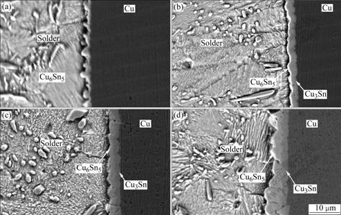
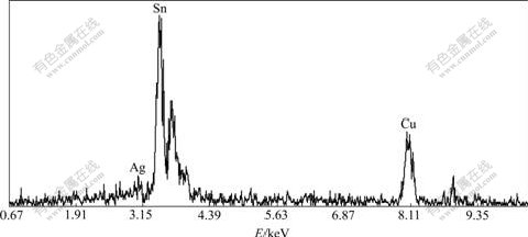
Fig.1 and Fig.2 show the SEM images of IMC layer of Sn-3.0Ag-0.5Cu-xCe(x=0, 0.1)/Cu substrate after soldering and aging. Fig.1(a) and Fig.2(a) illustrate that during the initial soldering (no aging), IMC layers are composed of Cu substrate, the intermetallic phases formed in the solder/Cu interface and the solder. In the as-soldered alloy system, the scallop-shaped IMC located at the solder/Cu interface is identified to be Cu6Sn5 by means of EDS analysis (Fig.3 and Table 1). The growth of IMC towards liquid solder results in coarse micrograph between IMC and solder, whereas its growth orientation is primarily uniform, which is mostly vertical to the solder. However, after aging for 120 h, another IMC is found between Cu substrate and Cu6Sn5. This Cu-Sn intermetallic compound is identified to be Cu3Sn by EDS as shown in Fig.4 and Table 2. The Cu3Sn film always forms at a relatively planar interface shown in

Fig.1 SEM images of IMC layer of Sn-3.0Ag-0.5Cu solder/Cu substrate at 443 K for various aging times: (a) As-soldered; (b) 120 h; (c) 240 h; (d) 480 h

Fig.2 SEM images of IMC layer of Sn-3.0Ag-0.5Cu-0.1Ce solder/Cu substrate at 443 K for various aging times: (a) As-soldered; (b) 120 h; (c) 240 h; (d) 480 h
Table 1 EDS results of IMC layer of Sn-3.0Ag-0.5Cu-0.1Ce/ Cu substrate (no aging)

Table 2 EDS result of IMC interface of Sn-3.0Ag-0.5Cu- 0.1Ce/Cu substrate (aging for 120 h)

Fig.1(b) and Fig.2(b). After aging for 240 and 480 h respectively, the thickness of the total intermetallic compound of Cu6Sn5 and Cu3Sn layers increases with increasing aging time. On the other hand, after aging for several days, a continuous and plane IMC layer forms. The thickness of both Cu6Sn5 and Cu3Sn IMC layers in Sn-3.0Ag-0.5Cu- 0.1Ce solder alloy is smaller than that in Sn-3.0Ag-0.5Cu alloy. Consequently, the total layer thickness of the Sn-3.0Ag-0.5Cu-0.1Ce alloy is also reduced.
3.2 Kinetic analysis of effect of Ce on growth of IMC
Generally, the thickness of the total intermetallic
compound formed in the aging process can be expressed by the simple parabolic equation[5, 10-11 ]:
Y=ktn (1)
where Y is the thickness of the reaction layer, k is the growth rate constant, n is the time exponent and t is the reaction time.
If the growth process is controlled by diffusion mechanism, the increase of the intermetallic compound layer after aging should follow the law of square root of time, Y =ktn. It is empirically found that n takes the value of 0.5 when the reaction is mainly controlled by diffusion mechanism[12].
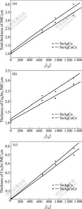
Fig.5 shows the total thickness of IMC, Cu6Sn5 and Cu3Sn vs the square root of aging time. The straight lines are obtained from the graphs of thickness vs square root of aging time. The mean thickness of the intermetallic compound layer(Y) of Cu6Sn5 and Cu3Sn as a function of the square root of the reaction time suggests that a thermally activated diffusion process has taken place for the growth of intermetallic layers in the Sn-3.0Ag-0.5Cu- xCe (x=0, 0.1) system. On the other hand, the growth speed of the intermetallic compound in the Sn-3.0Ag-0.5Cu/Cu system is faster than that in the Sn-3.0Ag-0.5Cu-0.1Ce/Cu system.

Fig.3 EDS line analysis of IMC layer of Sn-3.0Ag-0.5Cu-0.1Ce/Cu substrate without aging

Fig.4 EDS line analysis of IMC layer of Sn-3.0Ag-0.5Cu-0.1Ce/Cu substrate after aging for 120 h

Fig.5 Thickness of IMC layer of Sn-3.0Ag-0.5Cu-xCe(x=0, 0.1)/Cu substrate: (a) Total Cu6Sn5 and Cu3Sn IMC; (b) Cu6Sn5; (c)Cu3Sn
In order to approve growth behavior of the intermetallic compound, the growth rate constant(k) was calculated from a linear regression analysis of Y vs t1/2, where the slope equals k. Table 3 lists the growth rate constants calculated for total intermetallic compound (Cu6Sn5+Cu3Sn), Cu6Sn5 and Cu3Sn in the two solders system at different aging times. Compared with various k, it is found that the growth rate of the intermetallic compound in Sn-3.0Ag-0.5Cu/Cu system is faster than that in Sn-3.0Ag-0.5Cu-0.1Ce/Cu system during the aging at a constant temperature. Most of the linear correlation coefficient values (R2) for these plots are greater than 0.98. This confirms that the growth of the intermetallic compound layers is diffusion-controlled in the studied time range.
To evaluate the time exponents, the growth kinetics during aging at a constant temperature is represented by
Yt=Atn+Y0 (2)
where t is the reaction time, Yt is the layer thickness at t, A is a constant, n is the time exponent, and Y0 is the layer thickness at t=0. Eqn.(2) is converted into a logarithmic expression:
ln (Yt-Y0)=n ln t+ln A (3)
Fig.6 shows the plot of ln (Yt-Y0) vs ln t. The time exponent, n, is obtained from the slope of the plot of ln (Yt-Y0) vs ln t, and listed in Table 3. The diffusion processes appear to be largely responsible for growth of the intermetallic compound layer, although the time exponent is not exactly 0.5.

Fig.6 Plot of ln (Yt-Y0) vs ln t
Table 3 Calculated square of growth rate constants (k2), linear correlation coefficients (R2) and time exponent (n)

In Sn-3.0Ag-0.5Cu-xCe (x=0, 0.1)/Cu system, the forming process of IMC is divided into two steps. In the first step the IMC forms between Cu substrate and liquid solder in the soldering process and the second step is that the IMC forms between Cu substrate and solid solder after soldering. The formation and growth of IMC generate chiefly at the Cu/IMC interface. Therefore, the formation of IMC depends on the diffusion of Sn and Cu through the IMC layer to form new IMC. When the mass ratio of Sn to Cu is 6?5, Cu6Sn5 forms. If Sn atoms are in short supply and the mass ratio of Cu to Sn is 3?1, Cu3Sn may be observed[13]. According to the diffusion kinetics, the driving force for the IMC formation is dependent on the activity of its constituent elements[14-16]. For Cu-Sn IMC, the formation of driving force, that is, the Gibbs free energy, is dependent on the activity of Cu and Sn at the interface in solder alloy system. Lowering the activity and reducing the diffusion of Cu and Sn will be an effective method to depress the growth of the Cu-Sn IMC interface. The effect of Ce on the activity in Sn-Ag-Cu system was analyzed. The analytic results show that Ce has a higher affinity for Sn in the Sn-Ag-Cu system[17-18]. There is a larger possibility for Ce and Sn elements to form a compound and then the activity of Sn will be lowered. Compared Sn-3.0Ag-0.5Cu/Cu system with Sn-3.0Ag-0.5Cu-0.1Ce/ Cu system in this work, it is found that the thickness of IMC in the latter is smaller after aging. Since adding a small amount of rare earth element Ce into Sn-3.0Ag-0.5Cu solder can lower the activity of Sn at the interface and reduce the driving force for Cu-Sn IMC formation, then it will be helpful to depress the growth of Cu-Sn IMC. The results provide a new method to develop solder alloy with a high reliability.
4 Conclusions
1) With increasing aging time, two intermetallic compound layers, Cu6Sn5 and Cu3Sn, form, and the thickness of IMC increases at the interface in Sn-3.0Ag-0.5Cu-xCe (x=0, 0.1)/Cu solder alloy system. The growth rate of the IMCs in Sn-3.0Ag-0.5Cu/Cu system is faster than that in Sn-3.0Ag-0.5Cu-0.1Ce/Cu system. The thickness of the IMC in Sn-3.0Ag-0.5Cu/Cu system is greater than that in Sn-3.0Ag-0.5Cu-0.1Ce/Cu system. By adding 0.1% rare earth element Ce into the Sn-3.0Ag-0.5Cu solder alloy, the thickness of the Cu3Sn and Cu6Sn5 IMC interface layers of solder alloy system is reduced.
2) The growth process of intermetallic compound Sn-3.0Ag-0.5Cu-xCe (x=0, 0.1)/Cu system is controlled by diffusion mechanism, the increase of the intermetallic compound layers after aging follows the law of square root of time, i.e. Y=kt0.5.
References
[1] KIM K S, HUH S H, SUGANUMA K. Effects of fourth alloying additive on microstructures and tensile properties of Sn-Ag-Cu alloy and joints with Cu [J]. Microelectronics Reliability, 2003, 43(2): 259-267.
[2] CHEN W T, LEE S W, YIP M C. Mechanical properties and intermetallic compound formation at the Sn/Ni and Sn-0.7wt%/Ni joints [J]. Journal of Electronic Materials, 2003, 32(11): 1284-1289.
[3] YU D Q, WANG L. The growth and roughness evolution of intermetallic compounds of Sn-Ag-Cu/Cu interface during soldering reaction [J]. Journal of Alloys and Compounds, 2008, 458(4/2): 542- 547.
[4] GHOSH G. Interfacial microstructure and the kinetics of interfacial reaction in diffusion couples between Sn-Pb solder and Cu/Ni/Pd metallization [J]. Acta Materialia, 2000, 48(14): 3719-3738.
[5] LI Xiao-yan, YAN Yong-chang, SHI Yao-wu. Influence of IMC on the interface failure of Sn-Ag-Cu/Cu solder joint [J]. Journal of Mechanical Strength, 2005, 27(5): 666-671.
[6] YU D Q, WU C M L, LAW C M T, WANG L, LAI J K L. Intermetallic compounds growth between Sn-3.5Ag lead-free solder and Cu substrate by dipping method [J]. Journal of Alloys and Compounds, 2005, 392(1/2): 192-199.
[7] YOON J W, KIM S W, JUNG S B. Interfacial reaction and mechanical properties of eutectic Sn-0.7Cu/Ni BGA solder joints during isothermal long-term aging [J]. Journal of Alloys and Compounds, 2005, 391(1/2): 82-89.
[8] MA X, QIAN Y Y, YOSHIDA F. Effect of La on the Cu-Sn intermetallic compound (IMC) growth and solder joint reliability [J]. Journal of Alloys and Compounds, 2002, 334(1/2): 224-227.
[9] WUA C M L. Properties of lead-free solder alloys with rare earth element additions [J]. Materials Science and Engineering Report, 2004, 44: 1-44.
[10] YOON J W, JUNG S B. Investigation of interfacial reactions between Sn-5Bi solder and Cu substrate [J]. Journal of Alloys and Compounds, 2003, 359(1/2): 202-208.
[11] YOON J W, LEE Y H, KIM D G, KANG H B, SUH S J, YANG C W, LEE C B, JUNG J W, YOO C S, JUNG S B. Intermetallic compound layer growth at the interface between Sn-Cu-Ni solder and Cu substrate [J]. Journal of Alloys and Compounds, 2004, 381(1/2): 151-157.
[12] HIROSHI N, JIN Y P, TADASHI T. Interfacial reaction between Su-0.7Cu(-Ni) solder and Cu substrate [J]. Journal of Electronic Materials, 2006, 35(5): 1127-1132.
[13] PAKASH K H, SITHARAN T. Interface reaction between copper and molten Sn-Pn solders [J]. Acta Materialia, 2001, 49(13): 2481-2489.
[14] LI Bo, SHI Yao-wu, LEI Yong-ping. Effect of rare element addition on the microstructure of Sn-Ag-Cu solder joint [J]. Journal of Electronic Materials, 2006, 34(3): 217-224.
[15] TU X N, THOMPSON R D. Kinetics of interfacial reaction in bimetallic Cu-Sn thin films [J]. Acta Metallurgica Materialia, 1982, 30(5): 947-952.
[16] LAW C M T, WU C M L, YU D Q. Microstructure, solderability, and growth of intermetallic compounds of Sn-Ag-Cu-Re lead-free solder alloys [J]. Journal of Electronic Materials, 2006, 35(1): 89-93.
[17] BO Song-bai, CHEN Yan, L? Xiao-chun. Thermodynamics calculation and preliminary of the Sn-Ag-Cu-Ce Lead-free solder [J]. Transactions of the China Welding Institution, 2005, 26(5): 20-22.
[18] BO Song-bai, CHEN Yan, L? Xiao-chun. The calculation and application of activity interaction parameter in the Lead-free solder [J].Transactions of the China Welding Institution, 2005, 26(4): 45-47.
(Edited by YANG Hua)
Foundation item: Project(06GK2002) supported by the Major Project of Hunan Provincial Science and Technology Development Strategy
Received date: 2007-11-26; Accepted date: 2008-01-21
Corresponding author: LU Bin, PhD, Professor; Tel : +86-731-8836319; E-mail: luoffice@mail.csu.edu.cn