J. Cent. South Univ. (2017) 24: 2572-2581
DOI: https://doi.org/10.1007/s11771-017-3671-x

Impact of low/high-κ spacer–source overlap on characteristics of tunnel dielectric based tunnel field-effect transistor
JIANG Zhi(蒋智), ZHUANG Yi-qi(庄奕琪), LI Cong(李聪), WANG Ping(王萍), LIU Yu-qi(刘予琪)
School of Microelectronics, Xidian University, Xi’an 710071, China
 Central South University Press and Springer-Verlag GmbH Germany, part of Springer Nature 2017
Abstract: The effects of low-κ and high-κ spacer were investigated on the novel tunnel dielectric based tunnel field-effect transistor (TD-FET) mainly based upon ultra-thin dielectric direct tunneling mechanism. Drive currents consist of direct tunneling current and band-to-band tunneling (BTBT) current. Meanwhile, tunneling position of the TD-FET differs from conventional tunnel-FET in which the electron and hole tunneling occur at intermediate rather than surface in channel (or source-channel junction under gate dielectric). The 2-D nature of TD-FET current flow is also discussed that the on-current is degraded with an increase in the spacer width. BTBT current will not begin to play part in tunneling current until gate voltage is 0.2 V. We clearly identify the influence of the tunneling dielectric layer and spacer electrostatic field on the device characteristics by numerical simulations. The inserted Si3N4 tunnel layer between P+ region and N+ region can significantly shorten the direct and band-to-band tunneling path, so a reduced subthreshold slope (SS) and a high on-current can be achieved. Above all the ambipolar current is effectively suppressed, thus reducing off-current. TD-FET demonstrates excellent performance for low-power applications.
Key words: tunnel dielectric based tunnel field-effect transistor; tunnel field-effect transistor band-to-band tunneling; tunneling dielectric layer; subthreshold slope; off-current; on-current
1 Introduction
With the recent demonstrations of sub-60 mV/decade subthreshold slope (SS) and tunnel field-effect transistor (TFET) like low off-currents at room temperature, TFET has gained intensely investigation for low-power applications [1–8]. The demonstrated TFET devices have smaller bulk geometries than metal oxide semiconductor field-effect transistor (MOSFET), the configurations of TFET usually are ultra-thin body (body thickness <10 nm) and double gate [9–16]. Instead of applying the electric field, the drive current is generated by carriers tunneling from the valence or conduction band at the upper point in channel. So, TFET devices can overcome 60 mV/decade limit. However, many experimental results have illustrated that TFET devices suffer from severe ambipolar current and poor drive current [17–20].
In order to improve its on-current and suppress its ambipolar current, tunnel dielectric based tunnel field- effect transistor (TD-FET) and high-κ gate dielectric were reported by using Si3N4 dielectric between P+ region and N+ region [21]. In this brief, TD-FET with ultra-thin body, high-κ gate dielectric and dielectric tunnel layer are proposed to enhance the on-current, suppress the ambipolar current, and obtain a smaller subthreshold slope.
Although a very promising TD-FET structure has many advantages, it is still not clear about direct tunneling and BTBT impact output characteristics. To understand the TD-FET device operation, a detailed investigation on the impact of spacer–source overlap and electron–hole barrier tunneling (eBT and hBT) on tunnel layer electrostatic field and tunneling current is made. In this work, the influence of spacer and tunnel dielectric layer on tunneling current is clearly explained.
2 Devices structure and physical models
The devices analyzed in this work are TD-FETs built as double gate and P+-dielectric-N+. In contrast, the structures of conventional TFET and TD-FET are identical, including doping concentrations and geometry. But in spacer of TD-FET analysis, a low-κ dielectric spacer and a high-κ dielectric spacer are the only difference, as shown in Fig. 1. A uniform doping profile is used for N+ and P+ regions; the N+ doped (1×1019 cm–3) zone serves as drain and the P+ doped (1×1019 cm–3) zone serves as source (For TFET, channel doping is 1×1016 cm–3). A 2 nm high-κ gate dielectric HfO2 and 10 nm body-thickness are utilized for optimized subthreshold slope and on-current. The work function chosen for the gate contact is 4.7 eV. Si3N4 tunnel layer width is 1 nm. Throughout this work we assume drain supply voltage VDS=1.0 V. This work, focuses on the double gate TD-FET. A low-κ and high-κ dielectric spacer are used for devices output characteristics analysis. The simulation results are obtained by using Sentaurus TCAD tools. A nonlocal BtBT model, a direct tunneling model, a band-gap narrowing model, a drift–diffusion model and a density gradient model are included in simulation.

Fig. 1 Simulated TD-FETs:(All the gate dielectric is HfO2 and the tunnel layer width of Si3N4 is 1 nm)
Direct tunneling is the main tunneling mechanism for tunnel layer thinner than 2 nm. The computation of the tunneling probabilities is based on the Wentzel- Kramers-Brillouin (WKB) approximation [22]. The electron and hole tunneling probabilities (Te-CC and Th-VV) relate to the local wave numbers and the interface transmission coefficients (GCC and GVV). Two-band dispersion relation is most useful when direct tunneling is simultaneous with BTBT. The electron and hole tunneling probabilities in direct tunneling can be written as

 (1)
(1)

 (2)
(2)
where ε is a particle energy; position u>l (tunnel layer is 1 nm). In the two-band dispersion relation, κV replaces κCV and κVV, and  , where
 (3)
(3)
 (4)
(4)
where ECV and EVV are conduction and valence band energy shifted values, respectively. The simulations is a <100> orientation for the tunneling direction; mC is 0.328m0 and mV is 0.549m0 [23]. The interface transmission coefficients GCC and GVV can be calculated as
 (5)
(5)
 (6)
(6)
where vCC and vVV denote the velocities of electron and hole with energy ε on the beginning side of the tunneling barrier in conduction band and valence band, respectively; v+C and v+V denote the imaginary velocities on the end side of the tunneling barrier. If necessary, total tunneling current should also include BTBT contributions to tunneling current. The current density of electrons that tunnel from the valence band to the conduction band is the integral over the recombination rate. The total electron tunneling current density can be obtained:
 (7)
(7)
 (8)
(8)
 (9)
(9)
In Eqs. (8) and (9), the net electron recombination rate is


 (10)
(10)
And the net electron BTBT recombination rate is


 (11)
(11)
Analogously, the total hole tunneling current density is
 (12)
(12)
where jVV (l) is the hole direct tunneling current part, and jVC (l) is BTBT tunneling current part. In the next section, the direct and BTBT generation rate based on theoretically calculated parameters is used for TCAD simulation software.
3 Results and discussion
3.1 Performance analysis of TD-FET
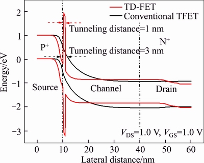
Figure 2 shows the simulated current–voltage characteristics of the TD-FET and conventional TFET. Due to the tunneling dielectric (TD) layer Si3N4, the tunneling carriers cannot penetrate easily through the TD layer at negative gate voltage. It can be clearly seen from Fig. 2 that the ambipolar current can be restrained effectively. The performance improvement of TD-FET can be explained by representing in Fig. 3. Tunneling distance of TD-FET device is obvious shorter than that of conventional TFET, and depends on the TD layer thickness. For TD layer thinner than 2 nm, the electrons and holes direct tunneling is the main tunneling mechanism at gate oxide layer and TD layer field is higher than 6 MV/cm. We found that the electric field of TD layer has more strength in centre than surface of the channel.

Fig. 2 Drain current versus gate voltage characteristics for a TD-FET and a n-type TFET at VDS=1.0 V and with source side and drain side spacer 5 nm

Fig. 3 Simulated energy band diagram in channel intermediate at VGS=1.0 V and VDS=1 V for n-type TFET and TD-FET
3.2 Effects of variation in spacer widths and high/low-κ
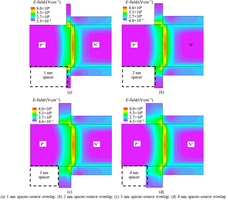
Four different spacer widths and low-κ spacer have been investigated in Fig. 4. The operation of the dielectric tunneling TD-FET is based on the both sides of conduction band or valence band energy level of Si3N4 tunneling barrier. To verify tunneling position and contribution of BTBT, electric-field in TD layer is shown in Fig. 4 for the 1, 2, 3 and 4 nm source–spacer overlap at VDS=1.0 V and VGS=1.0 V (the drain–spacer overlap has little influence on the performance of TD-FET, so it is not shown here). As shown in Fig. 4, electric-field in middle of TD layer has the most strength, and the direct tunneling and BTBT take place at the middle of channel. The characteristic of TD-FET differs from conventional TFET. It can be clearly seen that the electric-field in middle of TD layer decreases with increasing spacer width from Figs. 4(a) to (d). It can be explained that the spacer causes fringe-induced field effect which reduces the electric-field of channel [24]. The longer the spacer is, the more obvious the fringe-induced field effect is. The effect will not affect electron barrier tunneling (eBT) until spacer width of 5 nm. On the other hand, the simulated electron barrier tunneling rates are shown in Fig. 5 for the 1, 2, 3 and 4 nm source-spacer overlap at VDS=1.0 V and VGS=1.0 V. A comparison of the eBT rates among different spacer widths is shown in Fig. 5. With an increased spacer width, the eBT would decrease simultaneously. Due to the large tunneling area, carrier tunneling of TFETs only happens at surface in channel. It is the second reason that the drive current in TD-FET is larger than that in conventional TFET.
Compared to low-κ dielectric spacer, the high-κ dielectric spacer leads to more fringe-induced field in spacer as shown in Fig. 6. The electric field strength of TD layer with high-κ spacer would reduce more than that of TD layer with low-κ spacer. The maximum of the electric field also reduces in the middle of TD layer, consequently. Meanwhile, Figs. 7(a)–(d) display that the tunneling area and the maximum eBT rate of high-κ spacer decrease, compared to low-κ spacer, respectively. As a result, both direct tunneling rate and BTBT rate are decreased as compared to the low-κ spacer.

Fig. 4 Electric field plot for a TD-FET at VDS=1.0 V and VGS=1.0 V for high-κ gate dielectric (HfO2) and low-κ dielectric (SiO2) spacer:
3.3 BTBT, eBT and hBT contribution to tunneling current
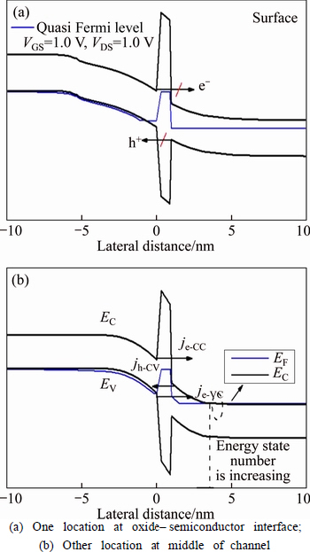
In this section, to better understand the TD-FET device operation, we investigate when BTBT current begins to get involved in total tunneling current by simulated band diagrams across the surface and middle of channel for three different gate voltages, as shown in Figs. 8–10. Based on the WKB approximation, tunneling probability should be equipped with enough high tunneling barrier. Besides, two sides carriers of tunneling barrier must have the same energy states occupied and unoccupied. Now, in order to distinguish the BTBT from the barrier tunneling, we refer to the eBT current as jCC and to the hBT current as jVV, respectively. In the same manner, we refer to the BTBT current as jCV or jVC. Owing to the same effects in the use of either high-κ or low-κ of gate dielectric and spacer, the case structure 3 is investigated in Section 2.
Unless otherwise mentioned, the structure 3 is used for our simulations. When the gate bias is lower than 0 V, the simulated energy band across channel–gate oxide interface and the middle of channel is shown in Fig. 9. The conduction band (EC) values of the channel region and P+ region are in the same level, and this condition results in no electron direct tunneling (jCC) and BTBT (jCV or jVC), as evident in Fig. 9(a). However, the valence band (EV) of channel region and P+ region have a certain number of hole energy states. Holes tunnel from the valence band of channel to the valence band of P+ region. The tunneling current flowing to the valence band of P+ region only contains the direct tunneling current (jh-VV) of holes that originate from the valence band of channel. Figure 9(b) shows the band diagram for the middle of channel. Due to non-existent hole empty states in P+ region and the lower-energy state occupied in channel, holes cannot effectively tunnel from valence band of P+ region to valence band of the channel. Under this condition, the conduction band of channel is above the quasi Fermi level. Analogously, electrons cannot effectively tunnel from conduction band of P+ region to conduction band of the channel, leading to non-existent electron tunneling (jCC). It may also be observed in Fig. 8(b) that EV of P+ region is effectively pinned by EC of channel region and as a result, the BTBT current would not happen at gate voltage of 0 V. In general, only hole direct tunneling contributes to the tunneling current under this condition.

Fig. 5 Electron barrier tunneling rate contours of TD-FET at VDS=1.0 V and VGS=1.0 V:
If VGS is further increased from 0.1 V to 0.2 V, the energy band as a function of lateral channel position is plotted in Fig. 9 for interface of the channel and gate oxide and the middle of channel at VGS=0.2 V and VDS=1.0 V. Figure 9(a) shows that the quasi Fermi level is under EC of channel at channel interface, and therefore, electrons of the P+ region impossibly tunnel to the channel. The channel valence band position is under the quasi Fermi level and there are no occupied energy states and unoccupied energy states on the two sides of TD layer. The direct current (jCC and jVV) would never flow at interface, as expected. It is observed in Fig. 9(a) that the BTBT current of electrons and the holes (jVC and jCV) would not happen, as aforementioned. The direct tunneling and BTBT characteristics at the middle of channel in the horizontal direction are also shown in Fig. 9(b). Under this condition, in turn, the quasi Fermi level is under EC of channel near the channel end. The holes BTBT current (jh-CV) now starts playing a role in the total tunneling current. The numbers of energy states occupied and unoccupied have risen greatly and the tunneling current has been improved effectively, leading to improving the subthreshold slope properties. At the same energy position, the tunneling distance of the holes tunnel from the middle of channel to the P+ region is 2.3 nm, as shown in Fig. 9(b). As the tunneling of the holes and the electrons come in pairs, the direct tunneling distance of the electrons is 1.3 nm from the TD layer. Note here that the holes BTBT current (jh-CV) and the electrons direct current (jh-CV) contribute to the total tunneling current. Finally, at VGS=1.0 V, the position quasi Fermi level is further increased from EC of channel at interface. The hole energy states occupied in channel do not exist, resulting in no direct tunneling and BTBT, which does not allow carriers tunnel across the TD layer at the surface of the channel. As VGS is further increased, the electric field of the TD layer increases gradually at the middle of channel. The BTBT of electrons and holes becomes appreciable at the middle of the channel, as shown in Fig. 10. Electrons and holes tunneling would not happen at the channel surface, as seen in Fig. 10(a). At the middle of the channel, the position between the quasi Fermi level and EC of the channel at VGS=1.0 V is larger than that at VGS=0.2 V. The electron tunneling starting point also gets closer to the TD layer, as shown in Fig. 10(b). The total tunneling currents consist of the eBT direct current (je-CC), electrons BTBT current (je-VC) and holes BtBT current (jh-CV). The BtBT current is an important part of the tunneling current, and carrier tunneling only takes place at the middle of the TD layer instead of the surface of the channel.

Fig. 6 Electric field plot for a TD-FET at VDS=1.0 V and VGS=1.0 V for high-κ gate and spacer dielectric (HfO2):
In order to generalize the above observations, the electric field in the TD layer of the TD-FET in the vertical direction is plotted in Fig. 11(a) for three values of VGS. For the electron barrier tunneling rate and the hole barrier tunneling rate, there are two different locations of the channel in the vertical direction: one at the TD layer–P+ region interface and the other at a distance of 1.3 nm from TD layer in the channel. When gate voltage is lower than 0.2 V, eBT would not occur nearby TD layer. However, the hBT rate is approximate 1017 cm–3·s–1, which is higher at the surface of the channel than at the middle of channel. Under the condition VGS=0.2 V and VDS=1.0 V, the holes tunneling current only consists of jh-CV. The electrons direct tunneling rate is larger than hBT rate (there is no eBT as discussed in Fig. 9(b)), as verified in Figs. 11(b) and (c). The currents of eBT and the hBT have more contribution to the tunneling current with the increasing of gate voltage. Finally, the electrons tunneling current consists of eBT current and electrons direct tunneling current; on the other hand, the holes tunneling current only has hBT current.

Fig. 7 Electron barrier tunneling rate contours of TD-FET at VDS=1.0 V and VGS=1.0 V for high-κ spacer:

Fig. 8 Simulated energy band diagram across channel at VDS=1.0 V and VGS=0.1 V:

Fig. 9 Simulated energy band diagram across channel at VDS=1.0 V and VGS=0.2 V:

Fig. 10 Simulated energy band diagram across channel at VDS=1.0 V and VGS=1.0 V:

Fig. 11 Different VGS corresponding to VDS=1.0 V for TD- FET:
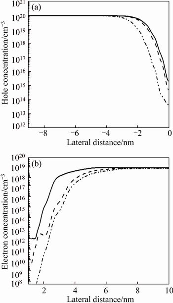
It also may be noted in Fig. 12(b) that the maximum electron concentration gets closer to the TD layer with an increase in gate voltage. On the other hand, the distance of a relatively high eBT rate also becomes smaller from TD layer, as observed in Fig. 8. Although the hole concentration at the interface of the TD layer and P+ region is low at such large value of gate voltage shown in Fig. 12(a), the strength of the TD layer electric field is relatively high, as observed in Fig. 7. Therefore, the eBT and hBT rates are also rather high.

Fig. 12 Hole concentration at three different gate voltages in the middle of channel (a) and electron concentration at three different gate voltages in the middle of channel (b)
4 Conclusions
We show the impact of source–spacer overlap on the output characteristics of a TD-FET. The fringe- induced fields can reduce the electric filed of the TD layer, leading to reducing the eBT rate and the hBT rate. The high-κ dielectric spacer leads to more fringe-induced fields. Further, tunneling current is studied when the BTBT plays a role in the total, and all parts of the tunneling current have been distinctly distinguished.
References
[1] BOUCART K, IONESCU A M. Double-gate tunnel FET with high-κ gate dielectric [J]. IEEE Trans Electron Devices, 2007, 54: 1725– 1733. DOI:10.1109/TED.2007.899389.
[2] ANGHEL C, CHILAGANI P, AMARA A. Tunnel field effect transistor with increased ON current, low-k spacer and high-κ dielectric [J]. Applied Physics Letters, 2011, 96: 12104. DOI: 10.1063/1.3367880.
[3] JIANG Z, ZHUANG Y Q. Drive current enhancement in TFET by dual source region [J]. Journal of Electrical and Computer Engineering, 2015, 905718. DOI: 10.1155/ 2015/905718.
[4] JIANG Z, ZHUANG Y Q. Impact of interface traps on direct and alternating current in tunneling field-effect transistors [J]. Journal of Electrical and Computer Engineering, 2015, 630178. DOI: 10.1155/2015/630178.
[5] SEO J H, YOON Y J. Design and analysis of Si-based arch-shaped gate-all-around (GAA) tunneling field-effect transistor (TFET) [J]. Current Applied Physics, 2015, 15: 208–212. DOI: 10.1109/ICOIN. 2016.7427155.
[6] VLADIMIRESCU HRAZIIA A, AMARA A. An analysis on the ambipolar current in Si double-gate tunnel FETs [J] Solid-State Electronics, 2012, 70: 67–72. DOI: 10.1016/j.sse.2011.11.009.
[7] HURKX G A M, KLAASSEN D B M. A new recombination model for device simulation including tunneling [J]. IEEE Trans Electron Devices, 1992, 39: 331–338. DOI: 10.1109/16.121690.
[8] IONESCU A M, RIEL H. Tunnel field-effect transistors as energy- efficient electronic switches [J]. Nature, 2011, 479: 329–337. DOI: 10.1109/IEDM.2015.7409755.
[9] FORD ALEXANDRA C, YEUNG C W, CHUANG S. Ultrathin body InAs tunneling field-effect transistors on Si substrates [J]. Applied Physics Letters, 2011, 98: 113105. DOI: 10.1063/ 1.3567021.
[10] RAJAMOHANAN B, MOHATA D. Insight into the output characteristics of III-V tunneling field effect transistors [J]. Applied Physics Letters, 2013, 102: 092105. DOI: 10.1063/ 1.4794536.
[11] CHIEN N D, VINH L T. Drive current enhancement in tunnel field-effect transistors by graded heterojunction approach [J]. Journal of Applied Physics, 2013, 114: 094507. DOI: 10.1063/1.4820011.
[12] MALLIK A, CHATTOPADHYAY A. The impact of fringing field on the device performance of a p-Channel tunnel field-effect transistor with a high-κ gate dielectric [J]. IEEE Trans Electron Devices, 2012, 59(2): 277–282. DOI: 10.1109/TED.2011.2173937.
[13] MALLIK A, CHATTOPADHYAY A. Tunnel field-effect transistors for Analog/Mixed-Signal system-on-chip applications [J]. IEEE Trans Electron Devices, 2012, 59(4): 888–894. DOI: 10.1109/ TED.2011.2181178.
[14] KAO K H, VERHULST ANNE S. Direct and indirect band-to-band tunneling in germanium-based TFETs [J]. IEEE Trans Electron Devices, 2012, 59(2): 292–301. DOI: 10.1109/TED. 2011.2175228.
[15] CHANG Hsu-Yu, ADAMS B. Improved subthreshold and output characteristics of source-pocket Si tunnel FET by the application of laser annealing [J]. IEEE Trans Electron Devices, 2013, 60(1): 92–96. DOI: 10.1109/TED.2012.2228006.
[16] LU Ye-qing, ZHOU Guang-le. Performance of AlGaSb/InAs TFETs with gate electric field and tunneling direction aligned [J]. IEEE Electron Device Letters, 2012, 33(5): 92–96. DOI: 10.1109/ LED.2012.2186554.
[17] WAN J, ZASLAVSKY C. A tunneling FETs on SOI: Suppression of ambipolar leakage, low-frequency noise behavior, and modeling [J]. Solid-State Electronics, 2012, 2011: 226–233. DOI: 10.1016/j.sse. 2011.06.012.
[18] MORITA Y, MORI T. Performance enhancement of tunnel field-effect transistors by synthetic electric field effect [J]. IEEE Trans Electron Devices, 2014, 35(7): 792–794. DOI: 10.1109/ LED.2014.2323337.
[19] KNOLL L, SCHMIDT M. Si tunneling transistors with high on-currents and slopes of 50 mV/dec using segregation doped NiSi2tunnel junctions [J]. Solid-State Electronics, 2013. 84: 211–215. DOI: 10.1016/j.sse.2013.02.028.
[20] GNANI E, GNUDI A. Drain-conductance optimization in nanowire TFETs by means of a physics-based analytical model [J]. Solid-State Electronics, 2013, 84: 96–102. DOI: 10.1016/j.sse.2013.02.012.
[21] LUO Z J, WANG H F. A tunnel dielectric-based tunnel FET [J]. IEEE Trans. Electron Devices, 2015, 36(9): 966–968. DOI: 10.1109/ LED.2015.2458932.
[22] ZHANG Q. LU Y Q. Optimum bandgap and supply voltage in tunnel FETs [J]. IEEE Trans Electron Devices, 2014. 61(8): 2174–2179. DOI: 10.1109/TED.2014.2330805.
[23] YANG Y, GUO P F. Simulation of tunneling field-effect transistors with extended source structures [J]. Journal of Applied Physics, 2012, 111: 114514. DOI: 10.1063/1.4729068.
[24] ALPIR C, MICHIELIS C D, PALESTRI P, SELMI L. Quantum mechanical study of the germanium election-hole bilayer tunnel FET [J]. IEEE Trans on Electron Devices, 2013, 60(9): 2754–2760. DOI: 10.11091TED.2013.22741.
(Edited by YANG Hua)
Cite this article as: JIANG Zhi, ZHUANG Yi-qi, LI Cong, WANG Ping, LIU Yu-qi. Impact of low/high-κ spacer–source overlap on characteristics of tunnel dielectric based tunnel field-effect transistor [J]. Journal of Central South University, 2017, 24(11): 2572–2581. DOI:https://doi.org/10.1007/s11771-017-3671-x.
Foundation item: Projects(61574109, 61204092) supported by the National Natural Science Foundation of China
Received date: 2016-02-29; Accepted date: 2016-10-08
Corresponding author: JIANG Zhi, PhD; Tel: +86-18984255877; E-mail: zjiang@xidian.edu.cn