Trans. Nonferrous Met. Soc. China 24(2014) 3158-3163
Giant magnetoresistance in Fe/SiO2/p-Si hybrid structure under non-equilibrium conditions
N. V. VOLKOV1, 2, A. S. TARASOV1, A. O. GUSTAJCEV1, 2, O. N. VOLKOVA2, S. N. VARNAKOV1, S. G. OVCHINNIKOV1, 2
1. Kirensky Institute of Physics, Russian Academy of Sciences, Siberian Branch, Krasnoyarsk 660036, Russia;
2. Institute of Engineering Physics and Radio Electronics, Siberian Federal University Krasnoyarsk 660041, Russia
Received 8 January 2014; accepted 20 April 2014
Abstract: The giant magnetoresistive (MR) effect was investigated in a simple Fe/SiO2/p-Si-hybrid-structure-based device from two back-to-back Schottky diodes. The effect was revealed only under the non-equilibrium conditions caused by optical radiation. It is demonstrated that the magnetoresistance ratio attains 100 or more. The main peculiarity of the MR behavior is its strong dependence on the magnitude and the sign of the bias current across the device and, most surprisingly, upon polarity of the magnetic field. It is important that the magnetoresistive effect is implemented exclusively in the subsystem of minority charge carriers transferred to the non-equilibrium states. The development of magneto-sensitive devices of this type can give grounds for a novel direction of semiconductor spintronics.
Key words: magnetoresistance; hybrid structure; Schottky diode
1 Introduction
Hybrid structures comprising classical semiconductors and magnetic materials are expected to be widely used in spintronics [1]. On one hand, magnetic structures find increasing application in magnetic recording. On the other hand, the properties of semiconductor materials are controllable in wide ranges by doping, electric field, or optical radiation, which determines the huge potential of modern semiconductor technology. Combining the magnetic and semiconductor structures can extend the functionality of hybrid- structure-based devices.
In our opinion, we are still far from using all merits of semiconductors in controlling the spin state and mutual transformation of the spin and charge currents in hybrid structures. As is well-known, when detecting the electric signal, one has to detect the change in the charge-carrier density. Obviously, with all other factors being equal, the minority carrier density is easier to be detected. This works equally well for the spin degrees of freedom: the variation in the spin state of minority carriers can be easily monitored. The density of such carriers can be changed, e.g. by transferring a system to the non-equilibrium state with the use of optical radiation. The spin polarization of the non-equilibrium photo- induced carriers can be effectively controlled by the optical selection rules for circularly polarized light [2], combination of the selection rules with photon energies [3], or even sub-picosecond electromagnetic pulses [4].
Here, we focus on the DC magnetotransport properties of the Fe/SiO2/p-Si hybrid structure with the Schottky barrier under the non-equilibrium conditions caused by optical radiation.
2 Experimental
The Fe/SiO2/p-Si structure was fabricated on a p-doped silicon wafer with a resistivity of 5 W��cm (a doping density of 2��1015 cm-3). The thicknesses of SiO2 and Fe layers were 1.2 and 5 nm, respectively. The details of structure preparation were described elsewhere [5]. The sample investigated was a simple well-known lateral device representing a circuit with back-to-back Schottky diodes. To fabricate the device, two electrodes separated by a 20-mm gap were formed from a continuous iron film on the structure��s surface. The device is schematically shown in Fig. 1. The desired topology of the electrodes was formed with a coordinatograph of original design using wet etching. On the top of the iron electrodes, ohmic contacts were formed using two-component silver epoxy.
DC resistance at a fixed current and the current�Cvoltage characteristics were measured in a current scanning regime. A magnetic field was applied in the structure plane perpendicular to the current direction. The optical effect was implemented using a laser diode with a wavelength of 980 nm. In the measurements, one of the ferromagnetic electrodes was exposed to linearly polarized light through a special optical window with 1 mm in diameter (Fig. 1).

Fig. 1 Schematic illustration of back-to-back Fe/SiO2/p-Si diode device and scheme of experiment (Shown setup of polarity is accepted as positive bias on device (+J))
3 Results and discussion
Figures 2(a) and 2(b) show the low-temperature dependences of resistance of the irradiated device. The dependences were obtained at bias current J of +20 and -20 mA in zero magnetic field and in the field H=��477 kA/m. The corresponding dependences of the photo-induced magnetoresistance (MR) ratio determined as Rph(0) and the resistances of the irradiated device in zero and nonzero magnetic fields, respectively are presented in Figs. 3(a) and (b). The selected J=+20 mA and J=-20 mA are conditioned by the maximum effect of the magnetic field at these biases. First of all, it is noteworthy that the huge value of the photo-induced MR effect can exceed by far 100 at H=477 kA/m. In the un-irradiated structure, the MR effect is not observed at all. Another surprising result is the extremely high sensitivity of the photo-induced MR effect to the polarity of field H. The asymmetry of the device photo- conductivity response relative to the signs of J and H can be clearly seen in the U-J characteristics (Fig. 4). At low temperatures, the U-J characteristic of the un-irradiated structure is symmetric and its shape is similar to the reverse characteristic of a tunnel MIS diode, i.e., the tunnel conductivity with the participation of the interface states is implemented [6]. When one of the MIS junctions is irradiated at H=0, the conductivity increases due to the photoconductivity processes involving the interface states. The latter participates in the formation of a photocurrent by sequential processes of tunneling or thermal generation and optical excitation of charge carriers. The growth of U at certain values of J is related to the current saturation determined by the non- equilibrium carrier density, i.e., the rates of generation and recombination of photoelectrons. The applied magnetic field of any polarity leads to the stronger growth of V to different extents, starting already from small values of J. Thus, the positive MR effect is implemented for all J values, independent of polarity (Fig. 5). It can be seen that the value of MR strongly depends on the value and sign of the bias current. At higher J, the photo-induced MR effect is suppressed and almost vanishes.
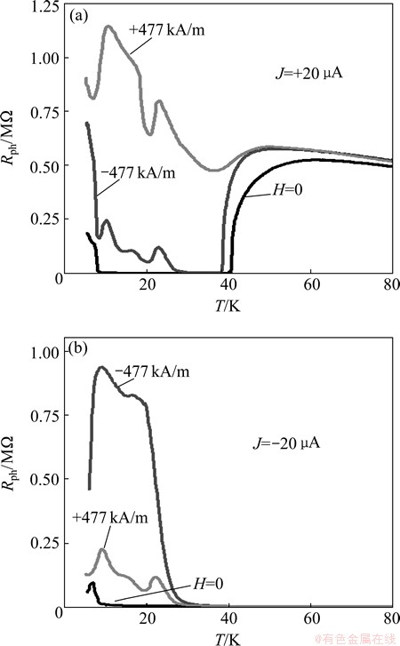
Fig. 2 Temperature dependences of resistance under optical radiation at J=+20 ��A (a) and J=-20 ��A (b) in zero magnetic field and in magnetic fields of +477 and -477 kA/m

Fig. 3 Appropriate temperature dependences of magneto- resistance measured at positive (a) and negative (b) bias currents

Fig. 4 U-J characteristic measured under optical irradiation in zero magnetic field and in magnetic fields of +716 and -716 kA/m
Figures 6(a) and (b) show the behavior of the dependences of (��R/R)ph on H at the high (J=��50 ��A) and low (J=��10 ��A) bias currents. Again, we see the asymmetry of the MR effect relative to the sign of both J and H. However, the behaviors of (��R/R)ph at high and low J are fundamentally different. At J=��10 ��A during the magnetic field scanning, the magnetoresistance first smoothly increases in the region of small H and then sharply grows above 239 kA/m. At J=��10 ��A and H=796 kA/m, it attains 1.5��103 and no saturation of the effect is observed. On the contrary, at J=��50 ��A, the sharp growth of starts from H=0 and slows down in the fields H=398-557 kA/m; with a further increase in the field, the MR effect tends to saturation. In this case, the maximum value of (��R/R)ph is no more than 400.
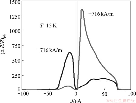
Fig. 5 Magnetoresistance vs bias current for positive and negative magnetic fields
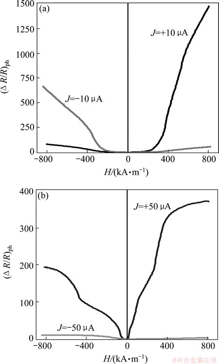
Fig. 6 Magnetoresistance as function of magnetic field for positive and negative bias currents of +10 and -10 ��A (a) and +50 and -50 ��A (b)
It can be seen that the photoconductivity response of the investigated device to the applied magnetic field appears nontrivial and depends on many factors. It is not excluded that there are several mechanisms working simultaneously. First of all, for the case of -J, the occurrence of the MR effect can be understood in the assumption that the magnetic field shifts the energy levels of the surface centers toward higher energies relative to the valence band. Indeed, at a certain temperature, the Fermi level (EF) approaches the energy levels of the interface state. As long as these levels are lower than EF, they participate in the optical transitions and photoelectrons ensure the high conductivity of the MIS junction and the entire device. At the expense of the shift in the magnetic field, the interface state levels are shifted higher than EF, capture holes and, consequently, stop participating in the generation of photoelectrons (Fig. 7(a)). The conductivity of the junction and the entire device drops.

Fig. 7 Schematic energy-band diagrams of MIS junction with surface states
The position of the interface state levels relative to EF depends also on the bias across the junction. The transport properties of the device were measured in the current stabilization regime. In this case, the problem of potential redistribution in the device at the variation in J is nontrivial. It is suggested that the growth of J results in the shift of the interface state levels upward relative to EF. This is possible, since the growth of the photocurrent through the junction should lead to the equalization of semiconductor and metal electrode potentials. Therefore, it is expected that the drop of T and the growth of H and J will complement one another. As the experiment shows, it is the fact. First of all, at small shifts, the large magnetic fields are required for the localized state levels to cross EF and get out from the process. On the contrary, at large biases, a part of the levels are already higher than EF and the rest ones start crossing EF already at small H (Figs. 6(c) and (d)).
Now, let us consider the situation when the irradiated MIS junction is located in the forward region of the U-J characteristic (+J). As in the previous case, the shift of the energy levels of the surface centers toward higher energies relative to the valence band in a magnetic field allows us to explain the occurrence of positive. The low resistance of the irradiated device at low temperatures is due to the switching on of the channel of electron tunneling between the metal and the surface state levels, if the latter coincides with EF in the metal. In the magnetic field, the levels appear higher than EF in the metal and get out from the tunneling process and, consequently, from the generation of photoelectrons (Fig. 7(b)). Thus, the conductivity of the device in the magnetic field decreases.
Regarding the bias dependence, the experiments show that the growth of J leads again to the shift of the localized surface state levels upward relative to EF, as can be expected with increasing negative bias voltage on the junction (negative potential on the metal electrode).
Recall that the phenomenon of the giant magnetoimpedance found by us in the similar back-to- back Fe/SiO2/p-Si diode device can also be explained with the mechanism that suggests the shift of the localized state level toward higher energies relative to the valence band of the semiconductor in a magnetic field. Moreover, the shift of the energy levels of impurity centers toward higher energies in a magnetic field was earlier observed in doped semiconductors, e.g., p-doped Si [7] and n�C-GaAs [8].
According to the impedance spectroscopy data [5], a magnetic field of 796 kA/m should result in the shift of the interface energy levels by at least 20 meV. This is the large value; for comparison, the Zeeman splitting for S=1/2 in a field of about 796 kA/m is no more than 0.1 meV. Which mechanisms are responsible for the corresponding change in the electron structure of the surface states? Possibly, it is the spin splitting of the surface states due to the effective exchange interaction with d electrons in a ferromagnet at the interface [9] or/and the exchange interaction with the localized magnetic centers in SiO2. Then, the magnetic field effect is reduced to magnetizing a ferromagnet or polarizing the localized magnetic centers.
Apart from the proposed mechanism, we do not exclude the possible contribution of the spin-dependent tunneling of photo-excited electrons through the SiO2 potential barrier to the ferromagnetic electrode. This process is determined by the spin polarization of photoelectrons and the details of the spin split density of states (DOS) in the ferromagnet. The spin polarization of photoelectrons can be controlled by a magnetic field, the exchange interaction with the magnetic impurity centers and circularly polarized light.
Obviously, none of the proposed models can explain the strong sensitivity of the photo-induced MR effect to the sign of H. It is necessary to use additional mechanisms of the magnetic field effect on the electron transport. In fact, there are not so many possible variants. First of all, an additional contribution to the MR effect dependent of the magnetic field polarity can be given by the Lorentz forces affecting energetic carriers [10]. When moving in a magnetic field, a carrier is affected by the force deflecting it in a certain direction. This direction depends on the direction of H and the direction of motion. In this case, at +J, photoelectrons move from one MIS junction to the other along the SiO2/p-Si interface in the device. Magnetic fields of different polarities deflect electron trajectories either in the direction of this interface or in the semiconductor volume. Since the recombination rates of photoelectrons near the interface and in the semiconductor volume are different, the photocurrent will have different values for the positive and negative polarity of a magnetic field.
There exists an alternative variant for explaining the dependence of MR on the applied magnetic field sign. This variant seems to be more interesting because it takes into account also the spin degrees of freedom of carriers. The mechanism involving the Rashba spin splitting effect is proposed [11], which can reach large values at the interfaces between Si and some materials [12]. The spin degeneracy elimination in the Rashba effect manifests itself during the motion of electrons in the potential gradient. The surface states can serve as electric field sources. Without going into details, we may consider that as a result of the Rashba effect, near the insulator/semiconductor interface, the number of electrons with the spin facing a specific direction increases and the spin current flows. The role of the field is reduced to magnetization reversal of the ferromagnetic electrodes, which serve as spin injector and detector. The dependence on the magnetic field sign is caused by the asymmetry arising at the injection of electrons with different polarization directions. Here, we demonstrate the possibility of such a mechanism. However, to discuss the details of its contribution to the photo-induced MR effect is still early.
4 Conclusions
The occurrence of the giant magnetoresistance effect caused by optical radiation in the device from two back-to-back Schottky diodes was demonstrated, which was fabricated on the basis of the Fe/SiO2/p-Si hybrid structure. For the first time, the MR effect in the hybrid structure was observed, which was determined by the behavior of the semiconductor subsystem of minority carriers in the non-equilibrium state formed by optical pumping. It is not improbable that the hybrid devices operating in this manner can give rise to a new concept in semiconductor spintronics.
Acknowledgments
This study was supported by the Presidium of the Russian Academy of Sciences (project No. 20.8); the Division of Physical Sciences of the Russian Academy of Sciences (project No. II.4.3); the Siberian Branch of the Russian Academy of Sciences (integration projects Nos. 43, 85 and 102); the RF Ministry for Education and Science (project No. 02.G25.31.0043); and the Russian Foundation of Basic Research (projects Nos. 14-02- 00234, 14-02-31156).
References
[1] FERT A. The present and the future of spintronics [J]. Thin Solid Films, 2008, 517: 2-5.
[2] STEINMULLER S J,  C M, WASTLBAUER G, BLAND J A C. Separation of electron spin filtering and magnetic circular dichroism effects in photoexcitation studies of hybrid ferromagnet/ GaAs Schottky barrier structures [J]. Phys Rev B, 2005, 72: 045301.
[3] KUREBAYASHI H, STEINMULLER S J,  J B, TRYPINIOTIS T, EASTON S, IONESCU A, YATES J R, BLAND J A C. Initial/final state selection of the spin polarization in electron tunneling across an epitaxial Fe/GaA(001) interface [J]. Appl Phys Lett, 2007, 91: 102114.
[4] WATZEL J, MOSKALENKO A S, BERAKDAR J. Photo-induced spin filtering in a double quantum dot [J]. Appl Phys Lett, 2011, 99: 192101.
[5] VOLKOV N V, TARASOV A S, EREMIN E V, VARNAKOV S N, OVCHINNIKOV SG, ZHARKOV S M. Magnetic-field- and bias-sensitive conductivity of a hybrid Fe/SiO2/p-Si structure in planar geometry [J]. J Appl Phys, 2011, 109: 123924.
[6] GREEN M A, KING F D, SHEWCHUN J. Minority carrier MIS tunnel diodes and their application to electron- and photo-voltaic energy conversion�CI. Theory [J]. Solid-St. Electron, 1974, 17: 551-561.
[7] SCHOONUS J J H M, BLOOM F L, WAGEMANS W, SWAGTEN H J M, KOOPMANS B. Extremely large magnetoresistance in Boron-doped silicon [J]. Phys Rev Lett, 2008, 100: 127202.
[8] HICKMOTT T W. Admittance measurements of magnetic freezeout in ntype GaAs [J]. Phys Rev B, 1992, 46: 12324.
[9] LUTSEV L V, STOGNIJ A I, NOVITSKII N N. Giant magnetoresistance in semiconductor/granular film heterostructures with cobalt nanoparticles [J]. Phys Rev B, 2009, 80: 184423.
[10] JOO S, KIM T, SHIN S H, LIM J Y, HONG J, SONG J D, CHANG J, LEE H W, RHIE K, HAN S H, SHIN K H, JOHNSON M. Magnetic-field-controlled reconfigurable semiconductor logic [J]. Nature, 2013, 494: 72-76.
[11] BYCHKOV Y A, RASHBA E I. Properties of a 2D electron gas with lifted spectral degeneracy [J]. Jetp Lett, 1984, 39: 78-81.
[12] GIERZ I, SUZIKI T, FRANTZESKAKIS E, PONS S, OSTANIN S, ERNST A, HENK J, GRIONI M, KERN K, AST C R. Silicon surface with giant spin splitting [J]. Phys Rev Lett, 2009, 103: 046803.
��ƽ��������Fe/SiO2/p-Si���Ͻṹ�ľ���ЧӦ
N. V. VOLKOV1, 2, A. S. TARASOV1, A. O. GUSTAJCEV1, 2, O. N. VOLKOVA2, S. N. VARNAKOV1, S. G. OVCHINNIKOV1, 2
1. Kirensky Institute of Physics, Russian Academy of Sciences, Siberian Branch, Krasnoyarsk 660036, Russia;
2. Institute of Engineering Physics and Radio Electronics, Siberian Federal University Krasnoyarsk 660041, Russia
ժ Ҫ���о��˻��ڼ�Fe/SiO2/p-Si�ṹ��2��ƴ��Schottky�����ܵľ���ЧӦ���þ���ЧӦֻ�ڹ���շ�ƽ�������²����֣��Ҵ����ʿɴﵽ100���ϡ��ô���ЧӦ�Ծ���������ƫ����С�뷽���Լ��ų����Ծ��и߶������ԡ�����Ҫ���Ǿ���ЧӦֻ�ڵ���ϵͳ�������������ת������ƽ��״̬��ʱ�����֡����ִ�����װ�ÿ�Ϊ�뵼����������һ���µķ�չ�����ṩ�ο���
�ؼ��ʣ����裻���Ͻṹ��Schottky������
(Edited by Yun-bin HE)
Corresponding author: N. V. VOLKOV; Tel: +7-391-2432635; E-mail: volk@iph.krasn.ru
DOI: 10.1016/S1003-6326(14)63455-5

