
Preparation of free-standing diamond films for high frequency SAW devices
LIU Jian-min(刘健敏)1, XIA Yi-ben(夏义本)1, WANG Lin-jun(王林军)1, SU Qing-feng(苏青峰)1, ZHAO Ping(赵 平)1, XU Run(徐 闰)1, PENG Hong-yan(彭鸿雁)2, SHI Wei-min(史伟民)1
1. School of Materials Science and Engineering, Shanghai University, Shanghai 200072, China;
2. Department of Physics, Mudanjiang Normal College, Mudanjiang 157012, China
Received 10 April 2006; accepted 25 April 2006
Abstract: Free-standing diamond films were prepared by hot filament chemical vapor deposition (HFCVD) method under different conditions. Inter-digital transducers (IDTs) were formed on the nucleation sides of free-standing diamond films by photolithography technique. Then piezoelectric ZnO films were deposited by radio-frequency(RF) reactive magnetron sputtering to obtain the ZnO/diamond film structures. Surface morphologies of the nucleation sides and the IDTs were characterized by means of scanning electron microscopy (SEM), atomic force microscope (AFM) and optical microscopy. The results indicate that the surfaces of nucleation sides are very smooth and the IDTs are of high quality without discontinuity and short circuit phenomenon. Raman spectra show the sharp diamond feature peak at about 1 334 cm-1 and the small amount of non-diamond carbon in the nucleation side. X-ray diffraction (XRD) patterns of the structure of ZnO/diamond films show a strong diffraction peak of ZnO (002), which indicates that as-sputtered ZnO films are highly c-axis oriented.
Key words: free-standing diamond film; surface roughness; ZnO thin film; surface acoustic wave devices
1 Introduction
With the development of mobile telephones, satellite broadcasting and wireless local area network systems, the demand for higher frequency surface acoustic wave (SAW) devices in GHz range is increasing day by day[1]. For SAW devices, the central frequency is determined by the equation f=V/λ, where f, V and λ are the center frequency, the SAW velocity and the wavelength, respectively. The wavelength l is determined by the size of inter-digital transducer (IDT). It is easy to understand that there are two approaches to achieve higher frequency operation: reducing the IDT size or using a substrate with higher propagation velocity. The first method requires expensive advanced lithography and limits the device power stability[2, 3]. Diamond, because of its high elastic modulus, has the highest acoustic velocity amongst all the materials. Due to its high sound velocity and excellent thermal conductivity, chemical vapor deposition (CVD) diamond combined with piezoelectric film, such as zinc oxide (ZnO) or aluminium nitride (AlN), is a promising material for high frequency SAW devices with sufficient power durability[4, 5].
There are three key elements for diamond SAW devices: good quality, low surface roughness for diamond film; high c-axis orientation for ZnO film[6].
In general, the growth side of polycrystalline CVD diamond, which is too rough, must be smoothed by mechanical or chemical polishing that is time-consuming and expensive[7]. Large surface roughness leads to wave scattering, propagation loss and discontinuity of the fingers of IDT. The nucleation side of free-standing diamond is very smooth[8]. In this work, the free-standing diamond film was fabricated and high quality inter-digital transducers (IDT) was deposited on the nucleation side. Furthermore, high (002) preferential orientation ZnO film was deposited on the nucleation side.
2 Experimental
Diamond films were prepared on mirror-polished n-type (100) silicon wafers by HFCVD technique using acetone carried by hydrogen. Two substrates were pretreated with diamond powder suspension in acetone in an ultrasonic bath for 30 min (conventional) and one substrate was mechanically scratched by hand with 100 nm diamond powder in water for about 30 min. Prior to depositing diamond film, the substrates were cleaned with hydrofluoric acid (HF) aqueous solution, deionized water, and acetone. The reaction conditions were as follows: substrate temperature 750-850 ℃, filament temperature 2 000-2 200 ℃, flux of acetone carried by hydrogen 50 mL/min, flux of hydrogen 180-200 mL/min. Diamond films with different quality were acquired by controlling different technique parameters. Other important growth parameters are listed in Table 1. After diamond deposition, the silicon substrates were etched in a dense mixture solution consisting of HNO3+HF to obtain free-standing diamond films. Then the films were chemically oxidized in H2SO4+H2O2 solution, rinsed and organically cleaned, in order to remove non-diamond carbon impurities.
Table 1 Deposition conditions (substrate pretreatment and growth parameters)

Photolithographic IDT consisting of Al electrodes whose size and distance of fingers were both 8 μm was formed on the nucleation side of sample 3# by lift-off technique and vacuum evaporation technology.
Then ZnO film was attempted to deposit on the nucleation side of sample 3# by radio-fregency(RF) magnetron sputtering. The air pressure in reaction chamber was pumped down to 3×10⁻³Pa prior to the induction of argon(99.999%). The sputtering conditions were as follows: sputtering power 400 W; gas pressure (0.2, 0.4, 0.6, 0.8, 1.0 Pa); substrate temperature: room temperature; time 1.5 h; target material ZnO ceramic.
The related characteristics of the films were analyzed by means of optical microscope (OLYMPUS BX60M), SEM (scanning electron microscope JSM-
6360LA), AFM(atomic force microscope AP-0190), Raman spectroscope(RH-800 type) and XRD(X-ray diffraction D/MAX-3C).
3 Results and discussion
SEM images for the nucleation side of frees-tanding diamond films are shown in Fig.1, from which it can be seen that nucleation sides are very smooth. For samples 1#, 2# and 3#, the mean size of nuclei is about 10, 4 and 0.3 μm, respectively. With the size of nucleus decreasing, the intervals between nuclei become more and more narrow.

Fig.1 SEM images for nucleation side of samples 1# (a), 2# (b) and 3# (c)
The nucleation density and surface roughness of nucleation side for samples 1#, 2# and 3# are listed in Table 2.
A typical atomic force microscope (AFM) image for the nucleation side of sample 3# is shown in Fig.2. The surface roughness is rather smooth and only about 1.5 nm. It is obvious that the nucleation side of sample 3# basically satisfies the requirements of surface roughness for high frequency SAW devices.
An image by optical microscope for IDT formed on the nucleation side of sample 3# is shown in Fig.3. It is obvious that the IDT is of high quality without discontinuity and short circuit phenomenon.
Table 2 Nucleation density and surface roughness of nucleation side for samples 1#, 2# and 3#
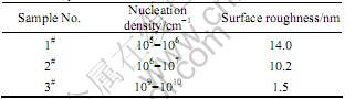

Fig.2 Typical 3D image of AFM for nucleation side of sample 3#

Fig.3 Optical microscope image for IDT on nucleation side of sample 3#
From the above results,it can be concluded that the nucleation under a lower gas pressure or the pre-
treatment of scratching silicon substrate by hand with nano-diamond powder will increase the nucleation density obviously, and therefore decrease the surface roughness. Firstly, very low pressure increases the mean free path of the reactive gas and therefore leads to an increase in the amount of atomic hydrogen and hydrocarbon species which impinge onto the substrate and create a more favorable environment for diamond nucleation. Secondly, since these species reach the substrate with a few collisions, the kinetic energy of these species remain high. This result in a large surface mobility, which promotes the aggregation of the precursors and improves the diamond nucleation[9]. Thirdly, abrasion by hand with diamond powder causes much more destruction on the Si surface than abrasion with diamond slurry in an ultrasonic generator, which might form a much higher density of sites suitable for diamond nucleation[10].
A typical Raman spectrum for the nucleation side of sample 3# is shown in Fig.4, from which it can be seen that a stronger Raman scattering peak exists at about 1 334 cm-1, characteristic of diamond, and a weaker Raman scattering band in the range from 1 400 to 1 600 cm-1, characteristic of non-diamond carbon. It is well known that the Raman scattering section of non-diamond carbon is bigger than that of diamond. The ratio of Raman scattering intensity is about 50∶1. So it is concluded that the nucleation side contains mostly diamond phase, and the content of the non-diamond phase is small, which shows a high quality diamond of the nucleation side.
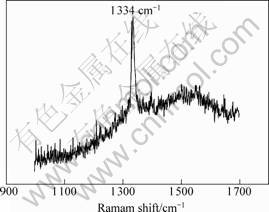
Fig.4 Typical Raman spectrum of nucleation side of sample 3#
Fig.5 shows the XRD patterns for ZnO/nucleation side of sample 3#, where the ZnO films are deposited by RF reactive magnetron sputtering technology under different reactive gas pressures. Sharp and strong peaks
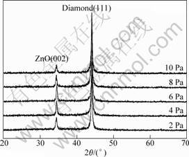
Fig.5 XRD patterns for ZnO/ nucleation side of sample 3# at different reactive gas pressures
exist around 34? and 44?, which are correlated to the characteristic peaks of zinc oxide (002) and diamond (111), respectively. The results show that highly c-axis oriented ZnO films can be deposited on nucleation sides of diamond films. The optimal reactive gas pressure is 0.6 Pa.
4 Conclusions
Free-standing diamond films are prepared by HFCVD method. IDTs are formed on the nucleation sides of diamond film by photolithography technique. ZnO thin films are deposited on nucleation side of free-standing diamond films by RF reactive magnetron sputtering. The results indicate that the nucleation under lower gas pressure or the pre-treatment of scratching silicon substrate by hand with nano-diamond powder will increase the diamond nucleation density obviously, and therefore decrease the surface roughness. The Raman spectrum shows a high diamond quality for the nucleation side of the free-standing diamond film. X-ray diffraction (XRD) patterns of the structure of ZnO/free-standing diamond film show sharp diffraction peaks for Zinc oxide (002), which indicates that the as-sputtered films are highly c-axis oriented. All results above suggest that the nucleation side of free-standing diamond film will be useful, ideal especially for developing a high frequency SAW device which requires a very smooth substrate surface for IDT patterns with a submicron size.
References
[1] ELHAD J D, XAVIE R L, DENIS R, et al. Growth process and surface acoustic wave characteristics of LiNbO3/Diamond/Silicon multilayered structures[J]. Jpn J Appl Phys, 2003, 42: 572-574.
[2] SHIKATE S, NAKAHATE H, HIGAKI K, et al. 1.5 GHz SAW bandpass filter using poly-crystalline diamond[A]. IEEE Ultrasonics Symp Proc[C]. Baltimore, MD, USA, 1993. 277-280.
[3] WANG S F, HSU Y F, PU J C, et al. Determination of acoustic wave velocities and elastic properties for diamond and other hard materials[J]. Materials Chemistry and Physics, 2004, 85: 432-437.
[4] BENEDIC F, ASSOUAR M B, MOHASSEB F, et al. Surface acoustic wave devices based on nanocrystalline diamond and aluminium nitride[J]. Diamond and Related Materials, 2004, 13: 347-353.
[5] SEO S H, SHIN W C, PARK J S. A novel method of fabricating ZnO/diamond/Si multilayers for surface acoustic wave (SAW) device applications[J]. Thin Solid Films, 2002, 416: 190-196.
[6] LAMARA T, BELMAHI M, ELMAZRIA O, et al. Free-standing CVD diamond elaborated by pulsed-microwave-plasma for ZnO/Diamond SAW devices[J]. Diamond and Related Materials, 2004, 13: 581-584.
[7] BENEDIC F, ASSOUAR M B, MOHASSEB F, et al. Surface acoustic wave devices based on nanocrystalline diamond and aluminium nitride[J]. Diamond and Related Materials, 2004, 13: 347-353.
[8] HUANG B, KE W. Surface properties on both sides of the isolated diamond film[J]. Mater Sci Eng B, 1999, B64: 187-191.
[9] JIAN K, CHAN Y X, YAN Y X, et al. Diamond nucleation and growth under very low-pressure conditions[J]. Diamond and Related Materials, 2000, 9: 1691-1695.
[10] MING R S, HAO W, ZHAO Y N. Enhanced diamond nucleation on pretreated silicon substrates[J]. Thin Solid Films, 1997, 301: 77-81.
(Edited by CHEN Wei-ping)
Foundation item: Projects(60577040) supported by the National Natural Science Foundation of China; Project(0404) supported by the Shanghai Foundation of Applied Materials Research and Development; Projects(0452nm051, 05nm05046) supported by the Nano-technology Project of Shanghai; Project(T0101) supported by the Shanghai Leading Academic Disciplines
Corresponding author: WANG Lin-jun; Tel: +86-21-56333514; Fax: +86-21-56332694; E-mail: ljwang@staff.shu.edu.cn

