Trans. Nonferrous Met. Soc. China 27(2017) 2104-2111
Nucleation interface of Al-Sb alloys on single crystal Al2O3 substrate
Lu WANG1,2, Lin YANG2, Di ZHANG1, Ming-xu XIA1, Yun WANG3, Bin CHEN1, Jian-guo LI1
1. School of Materials Science and Engineering, Shanghai Jiao Tong University, Shanghai 200240, China;
2. School of Materials and Engineering, Jiangsu University of Technology, Changzhou 213001, China;
3. BCAST, Brunel University, Uxbridge, Middlesex UB8 3PH, UK
Received 4 June 2016; accepted 4 January 2017
Abstract: Lattice structure information of heterogeneous nucleation at nucleation interface was present. The crystal orientation, and interfacial structure characteristic of liquid Al alloys nucleated on the basal surface (0001) Al2O3 single crystal substrate were identified by X-ray diffraction (XRD), scanning electron microscopy (SEM) and high resolution transmission electron microscopy (HRTEM) analysis. The preferred crystal orientations of pure Al and Al-1%Sb (mass fraction) alloy adjacent to the nucleation interface were examined as (200) and (220) planes of Al, respectively, and two corresponding orientation relationships were obtained. An improved nucleation efficiency and refined grains were attributed to both the reduced interplanar spacing of preferred orientation and the decrease of lattice misfit from 16.4% to 7.0% in Al-1%Sb/Al2O3 nucleation group.
Key words: aluminium alloy; nucleation; interfacial structure; orientation relationship
1 Introduction
Since the first undercooling measurement executed by FAHRENHEIT [1] on the solidification of supercooled water providing the evidence for nucleation barrier, the nucleation of liquid towards a more condensed state attracts extensive scientific interests and technological attentions due to the intimate relationship with initial structure, the size scale of the structure and spatial distribution [2]. It is common practice to introduce nucleating agents during the casting process in order to reduce cast defects, form fine and uniform grains and therefore improve casting quality.
The investigation of ordering phenomena at solid-liquid interface has been carried out by various theoretical and experimental approaches [3-6] from the last century. High resolution transmission electron microscopy (HRTEM) [7,8] enables direct imaging of various interfaces at the atomistic level. For an extensive review on the epitaxy growth of general film in Ref. [9], the experimental evidence of heterostructures was presented across various misfit scales. A good lattice matching at the interface and a small undercooling represent a potent nucleation potency of the nucleating substrate in Al/Al2O3 system [10]. While in aspect of grain refining, apart from nucleating agents such as Al-Ti-B in Al alloy and Al-Ti-C in Mg alloy [11-13], trace alloying element, RE, K, Na, Ca, Sr, Ba, Sn, Sb, Bi, P is also added into alloys as microstructure modifier [14-19]. In these elements, Sb is a surface-active element extensively used in Al-Si alloys, Mg-Al-Si alloys and Al-based composites [20-24], to modify eutectic structure forming at relatively high cooling rates for enhanced casting properties. There are a few works on the modification mechanism of Sb to Si, Mg2Si phases and so on. For example, REN et al [20] presented that the nucleation site of Mg2Si in Mg-Al-Si alloy, is enriched in Si, Mg and Sb. WANG et al [22] suggested that the coherent precipitation of AlSb can introduce stress into Si crystal forming little defects, which hinders the growth of Si. They further pointed out that Sb and Ba will enhance the modification effect of RE. To date, different modification mechanisms of Sb in Al-Si and Al-Mg-Si alloys have been achieved. However, there is very little information regarding the interface structure formed during both nucleation and solidification processes of common metal casting on the specific substrates, such as the usually existed oxide Al2O3 in Al alloy. Correspondingly, the nucleation efficiency and refinement effect of Sb element on the heterogeneous nucleation of Al hasn��t been investigated thoroughly yet.
This work aims at providing specific experimental results on nucleation behaviour of liquid Al-Sb alloy on a single crystal sapphire substrate and interfacial structure inspired by the nucleation is also investigated. The identity of nucleation interfacial structure is verified by multi-analytical technologies. Following that, the orientation relationships between the nucleation phase and substrate are experimentally determined through HRTEM. The enhanced nucleation efficiency and refining effect of Al-Sb alloy is hereupon evaluated from the crystallographic point of view, using a modified lattice matching model [25].
2 Experimental
A sapphire with basal surface (0001) was used for the nucleation substrate in this work. The surface roughness of the substrate was less than 5 nm. High purity Al (99.999%, mass fraction) was purified using glass fluxing method to remove potential heterogeneous nuclei from liquid Al. To examine alloying element effect on the nucleation behavior of liquid Al and the structure configuration of nucleation interface, Sb (99.999%, mass fraction) was added into liquid Al after purification. The mass fraction of 1% was selected to ensure primary ��-Al phase nucleated under an uninterfered environment, to avoid any interfere from the potential compounds, according to Al-Sb phase diagram [26]. Al-1%Sb (mass fraction) alloy was prepared by arc melting under an argon atmosphere, and then directly cast into cylindrical rods with 3 mm in diameter using a suction casting facility.
The Al2O3 substrate was firstly cleaned in acetone for 3 min with an ultrasonic cleanser and then placed on a gas cooling platform in a high vacuum chamber (the pressure was 2��10-4 Pa). Aluminum and its alloy samples were placed on such an Al2O3 substrate and then Al/Al2O3, Al-1%Sb/Al2O3 couples were heated up to 1300 K (1027 ��C) by a laser beam with a heating rate of 20 ��C/s. The sample was held at that temperature for 3 min before the laser beam was switched off, and then cooled down at a controlled cooling rate of 20 ��C/s under a flowing argon atmosphere. The details can be referred to Ref. [27]. X-ray diffraction (XRD) analysis was employed to detect the crystal orientation of newly formed crystal from the bottom of the sample where nucleation was triggered by the substrate. Scanning electron microscopy (SEM) samples were obtained through conventional metallurgical sample preparation procedure for microstructural analysis. SEM was executed with backscattered electron (BSE) mode by Phenom XL System coupled with energy dispersive X-ray spectroscopy (EDS) analysis. Interfacial structure investigations were carried out by transmission electron microscopy (TEM) and HRTEM using a Tecnai G2 F20 S-twin TEM instrument. The samples were prepared from cutting slices perpendicular to the interface with a thickness less than 80 ��m before ion beam thinned using a Gatan PIPS II precision ion polishing system at 5.0 kV and an incident angle of 4��-6��.
3 Results and discussion
3.1 Crystal orientation of nucleated phase
The crystal orientation of Al alloy adjacent to the nucleation interface was examined on Al/Al2O3(0001) and Al-1%Sb/Al2O3(0001) systems using XRD analysis, as shown in Fig. 1. The result shows that the preferred crystal orientation of pure Al was (200). When Sb was added into Al liquid, the preferred crystal orientation of newly formed crystals was changed into (220). Besides the crystals of Al matrix, the AlSb compound was also detected with the (111), (200), (220) and (311) diffraction peaks. It is obvious that the crystal orientation of new crystals nucleated on the (0001) Al2O3 substrate was affected by the addition of Sb.
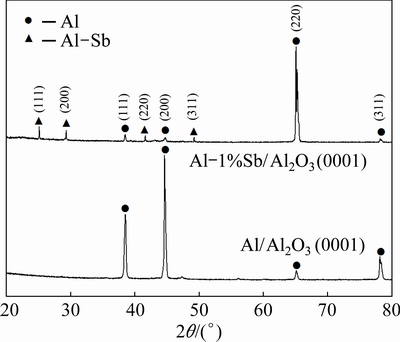
Fig. 1 Crystal orientation of newly formed crystals adjacent to interface in Al/Al2O3(0001) and Al-1%Sb/Al2O3(0001) systems
3.2 Interface characteristics
SEM images at crystal-substrate interfaces of Al/Al2O3(0001) and Al-1%Sb/Al2O3(0001) systems are presented in Fig. 2. It is seen that both the interfaces between crystal phases and Al2O3 substrate were straight and distinct. Two phases appeared in the Al-1%Sb crystals in Fig. 2(b) compared with only one phase in counterpart Al/Al2O3(0001) system in Fig. 2(a). The darker and brighter phases marked as ��1�� and ��2�� in Fig. 2(b), were confirmed as matrix Al and Al-Sb compound, respectively. While in Fig. 2(a), the phase was detected as Al. The compound in Fig. 2(b) formed either at the interface or in the matrix, both with thickness less than 5 ��m. The composition of the matrix, compound and substrate was qualitatively analyzed, as shown in Figs. 3(a)�C(c) as Al, Al-Sb phase and Al-O phase.
3.3 TEM and HRTEM analysis
The interfacial structure between Al and Al2O3 substrate has been systematically studied using TEM and HRTEM methods. Figure 4(a) shows a typical cross- sectional TEM bright-field image of Al/Al2O3(0001) interface. A sharp and straight interface split new crystal from lower substrate. Through selected area electron diffraction (SAED) examination, it was confirmed that the upper area corresponds to Al phase, while the below substrate is Al2O3.
Figure 4(b) displays a HRTEM image of Al/Al2O3(0001) taken along Al2O3 axis. The interplanar spacing in the upper area was consistent with the face-centred cubic structure of Al with spacings of 2.0296 and 2.0190
  both close to aAl/2, while spacing in the lower area was in accord with the hexagonal structure of Al2O3 with spacings of 2.3810 and 4.3553 , which are close to aS/2 and cS/3. The subscript ��S�� represents Al2O3 substrate. They respectively corresponded to planes {200} of Al in upper area and
  and {0003} of Al2O3 in lower area. Among them,
  and
and  were labelled in Fig. 4(b). It is noting that
  plane of Al2O3 is perfectly parallel to the interface and meanwhile the lattice arrangement of is identical to that of (0001). Therefore, the (0001) plane of Al2O3 is parallel to the interface. In addition, the incident beam was also aligned with [001]Al direction. According to the presented lattice image in Fig. 4(b), is approximately parallel to , with a small tilt angle.

Fig. 2 SEM images of Al/Al2O3(0001) (a) and Al-1%Sb/Al2O3(0001) (b) interfaces
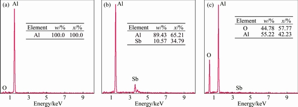
Fig. 3 EDS analysis results for matrix (a), compound (b) and substrate (c) as marked with ��1��-��3�� in Fig. 2(b)
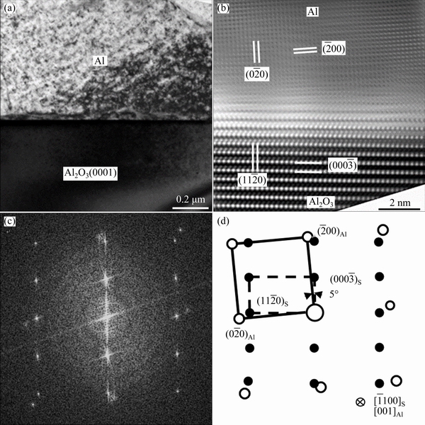
Fig. 4 Typical cross-sectional TEM bright-field image of Al/Al2O3(0001) interface (a), HRTEM of Al/Al2O3(0001) taken along Al2O3  axis (b), fast Fourier transformation (FFT) image of HRTEM (c), and schematic index of FFT pattern along
  and [001]Al zone axes, where open and filled circles represent Al and Al2O3 respectively (d)
The fast Fourier transformation (FFT) image is shown in Fig. 4(c) by making Fourier transform of the HRTEM. It is seen that there are two sets of diffraction spots, one set from Al2O3 and the other from Al. An orientation relationship (OR) between Al and Al2O3 can be obtained from the diffraction pattern. A schematic index of the pattern is shown in Fig. 4(d). With the help of FFT pattern, a 5�� tilting between the pair of parallel planes is determined. This 5�� tilt is clearly seen in Fig. 4(c) and (d) by the small misorientation between diffraction spots and . Therefore, an OR between Al2O3 and Al is established:  ~//[001]Al.
Figure 5(a) shows a typical cross-sectional TEM bright-field image of Al-1%Sb/Al2O3(0001) interface. A small particle with thickness about 300 nm was observed at the interface. The up and lower areas were confirmed as Al phase and Al2O3 substrate through SAED analysis in Fig. 5(b). The SAED pattern was taken from the area including substrate, small particle and Al matrix across the interface viewed along zone axis, which exhibits three clear sets of diffraction spots. Two sets with similar interplanar spacing appear periodically and the third set with the smallest interplanar spacing has only one group of symmetrical spots. A schematic index of the pattern is shown in Fig. 5(c).
The interplanar spacing of innermost spots, the filled circles, corresponded to hexagonal structure of Al2O3 with spacings of 2.3810 and 4.3553 , which are close to aS/2 and cS/3, and {0003} planes of Al2O3. The interplanar spacing for the set of outermost spots, the large open circles, was equal to the face-centred cubic structure of Al with spacings of 1.4180 and 1.2240 , which are close to aAl/2 and aAl/
 , {220} and {311} planes of Al matrix. It is indicated that the Al crystal is orientated along [114]Al zone axis. The middle set of spots was very close to the set of Al2O3, where the interplanar spacings are 3.5294 and 2.1490 for the two nearest spots from center spot. According to the XRD pattern in Fig. 1 and EDS result in Fig. 2, the small particle could be AlSb compound. AlSb is cubic ZnS structure with the lattice constant of 6.13 [26]. The two nearest spots could be {111} and {220} planes of AlSb, with its incident beam aligned along
  zone axis. The corresponding planes of diffraction spots were labelled in Fig. 5(c). Given (0001)S parallel to the interface and the SAED pattern illustrated in schematic image, it can be deduced that (0003)S is parallel to
  while the plane is approximately parallel to
  with a tilt about 8�� since the diffraction spot deviates from (0003)S, as indicated in Fig. 5(c). Therefore, an OR among the substrate, compound AlSb and Al matrix can be concluded as (0003)S//~ //[114]Al.
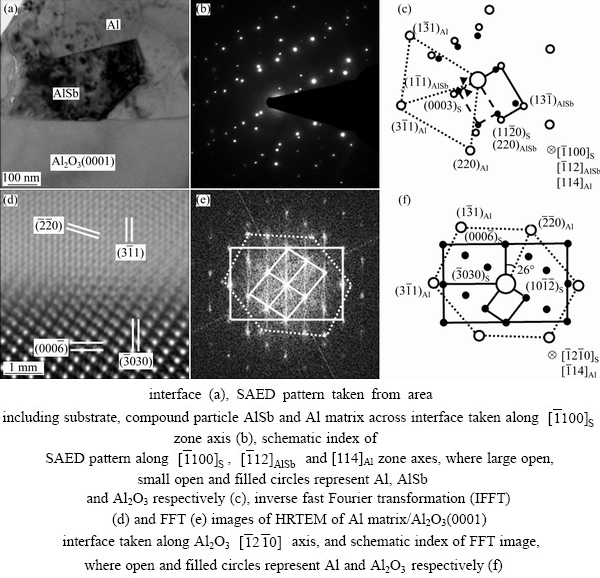
Fig. 5 Typical cross-sectional TEM bright-field image of Al-1%Sb/Al2O3(0001)
As Al matrix solidified at first and then the AlSb phase, the inverse fast Fourier transformation (IFFT) and FFT images were further investigated by the HRTEM of Al matrix/Al2O3(0001) interface, which are shown in Figs. 5(d) and (e) along Al2O3  axis. The schematic index of the FFT image is shown in Fig. 5(f). There are two sets of diffraction spots in Fig. 5(f), one set from Al matrix and the other from Al2O3, indicating the incident electron beam parallel to
  axis of Al2O3 and
  axis of Al matrix at the same time. The corresponding planes of Al matrix and Al2O3 are labelled in Figs. 5(d) and (f). It is seen that
  plane of Al2O3 is parallel to the interface, while
  plane of Al deviates from the interface with an angle about 26��. The matching directions are //
  and the matching planes at the interface are
  and
and  but with a 26�� tilting angle.
3.4 Lattice parameter and lattice misfit of different nucleated systems
According to the value of 2�� and diffraction spots in XRD and SAED patterns, the d-spacing of different crystal planes for Al and Al-Sb solid solution can be calculated and listed in Table 1. The ��+�� and ��-�� represent that experimental d-spacings of Al and Al-Sb solid solution are extended and compressed, respectively, compared with the referenced value d0 [28].
Table 1 d-spacings of different crystal planes for Al and Al-Sb solid solution combined with referenced value d0 [28]
For pure Al,  from SAED is extended to 2.0296 and
  is compressed to 2.0190 . That is because two sets of planes
  and
and  intersect at the interface and
  is larger than at the matching direction, which places the Al crystal under tensile stress. While all d-spacings from the XRD are extended a little, with the lattice expansion at high temperature and an average of {200} at different directions. For Al-Sb solid solution,
  from the SAED is reduced to 1.4180 and
  is increased to 1.2240 . Furthermore, d{220} from the XRD pattern is also decreased to 1.4293 , compared with the referenced d0. It is indicated that the contribution of Sb solution in Al to the decrease in {220} planes exceeds lattice expansion at high temperature and an average of {220} at different directions. The lattice parameter for Al and Al-Sb solution at the nucleation interface is calculated as 4.0590, 4.0380 and 4.0107 , respectively, based on interplanar spacing , and d{220} from SAED patterns.
Based on the data available in HRTEM and SAED patterns, the two-dimensional planar misfit (f) between nucleated crystals and substrate can be calculated using the modified Bramfitt equation [25]:
 (1)
(1)
where d[uvw]s and d[uvw]n are the interatomic spacings along direction [uvw]s and [uvw]n; �� is the angle between [uvw]s and [uvw]n; the subscripts ��s�� and ��n�� stand for substrate and nucleated crystal, respectively. It should be noted that planes of (hkl)s and (hkl)n used in this work are (0001) plane of Al2O3 and the preferred growth plane of newly nucleated phase in XRD pattern, and [uvw]s and [uvw]n are low index directions in these two planes.
For Al/Al2O3 system, the OR between Al and Al2O3 is ~//[001]Al. Reconstructing interface matching between and , it is easy to find the optimal planar matching units. Figure 6(a) shows the atomic arrangement for the interface matching of on schematically with the zone axis of  parallel to that of , leaving out the effect of the small tilt between the parallel planes. It is seen that a selected unit cell along and [010]Al directions of Al crystal badly matches with a unit cell of Al2O3 along
  and
and  of low index directions with a misfit of 16.4%.
Considering the solidification sequence of the Al-1%Sb alloy, where Al matrix will solidify first, the nucleation interface of Al-1%Sb/Al2O3 system will be / with XRD and HRTEM analysis. By reconstructing
  interface matching with the zone axis of parallel to that of and a tilt 26�� between and
  as shown in Fig. 6(b), an optimal misfit 7.0% between this interface can be obtained when a unit cell along and directions of Al2O3 matches a unit cell from the bottom planes along and
  of Al crystal well. An decrease of lattice misfit from 16.4% to 7.0% may occur when nucleation of Al liquid with addition of Sb on
  substrate.


Fig. 6 Schematic illustration of interface matching between  and
and  (a) and
  and
and  (b)
(b)
Therefore, the solution of Sb in Al results in the change of lattice parameter, the crystal orientation and even the lattice misfit of Al matrix crystals nucleated on the Al2O3(0001) substrate. Better nucleation efficiency and finer grains can be achieved as a result of the small lattice misfit after Sb turning the lattice structure of Al when it nucleated on the Al2O3 substrate.
4 Conclusions
1) The preferred crystal orientation of pure Al and Al-1%Sb alloy adjacent to the nucleation interface was examined as (200) and (220), respectively. Small AlSb compounds were identified either at the interface or in the Al matrix of Al-1%Sb alloy by XRD, SEM and TEM in combination with EDS and SADP analysis.
2) The evaluation by lattice matching model and the ORs determination by HRTEM confirm that alloy element Sb enhanced nucleation efficiency and refined grains of Al-1%Sb alloy through the reduced interplanar spacing of preferred orientation and tuned lattice misfit in Al-1%Sb/Al2O3 nucleation couple compared with Al/Al2O3 nucleation system.
References
[1] FAHRENHEIT D G. The experiments and observations of supercooled water in vacuum [J]. Philosophical Transactions of The Royal Society, 1724, 33: 78-84.
[2] MA Qian. Heterogeneous nucleation on potent spherical substrates during solidification [J]. Acta Materialia, 2007, 55: 943-953.
[3] BUTA D, ASTA M, HOYT J J. Atomistic simulation study of the structure and dynamics of a faceted crystal-melt interface [J]. Physical Review E, 2008, 78(3): 031605.
[4] KANG J, ZHU Jun-yi, CURTIS C, BLAKE D, GLATZMAIER G, KIM Y H, SU H W. Atomically abrupt liquid-oxide interface stabilized by self-regulated interfacial defects: The case of Al/Al2O3 interfaces [J]. Physical Review Letters, 2012, 108(22): 226105.
[5] OH S H, KAUFFMANN Y, SCHEU C, KAPLAN W D,  M. Ordered liquid aluminum at the interface with sapphire [J]. Science, 2005, 310(5748): 661-663.
[6] BARAM M, GAROFALINI S H, KAPLAN W D. Order in nanometer thick intergranular films at Au-sapphire interfaces [J]. Acta Materialia, 2011, 59(14): 5710-5715.
[7] LEE S B, KIM Y M. Direct observation of in-plane ordering in the liquid at a liquid Al/��-Al2O3 interface [J]. Acta Materialia, 2011, 59(4): 1383-1388.
[8] GANDMAN M, KAUFFMANN Y, KOCH C T, KAPLAN W D. Direct quantification of ordering at a solid-liquid interface using aberration corrected transmission electron microscopy [J]. Physical Review Letters, 2013, 110: 086106.
[9] NARAYAN J. Recent progress in thin film epitaxy across the misfit scale [J]. Acta Materialia, 2013, 61: 2703-2724.
[10] WANG L, YANG L, ZHANG D, XIA M, WANG Y, LI J G. The role of lattice misfit on heterogeneous nucleation of pure aluminum [J]. Metallurgical and Materials Transactions A, 2016, 47: 5012-5022.
[11] WANG Xue-jiao, XU Cong, MUHAMMAD A, HANADA S, YAMAGATA H, WANG Wen-hong, MA Chao-li. Effects of Al-Ti-B-RE grain refiner on microstructure and mechanical properties of Al-7.0Si-0.55Mg alloy [J]. Transactions of Nonferrous Metals Society of China, 2014, 24: 2244-2250.
[12] FAN Z, WANG Y, ZHANG Y, QIN T, ZHOU X R, THOMPSON G E, PENNYCOOK T, HASHIMOTO T. Grain refining mechanism in the Al/Al-Ti-B system [J]. Acta Materialia, 2015, 84: 292-304.
[13] LIU Xiao-teng, HAO Hai, ZHU Xiao-xu, ZHANG Xing-guo. Grain refining effect of Mg by novel particle cluster-containing Al-Ti-C master alloy [J]. Transactions of Nonferrous Metals Society of China, 2015, 25: 1804-1810.
[14] LI Chong, WU Yu-ying, LI Hui, LIU Xiang-fa. Microstructural formation in hypereutectic Al-Mg2Si with extra Si [J]. Journal of Alloys and Compounds, 2009, 477(1-2): 212-216.
[15] QIU Ke, WANG Ri-chu, PENG Chao-qun, WANG Nai-guang, CAI Zhi-yong, ZHANG Chun. Effects of Mn and Sn on microstructure of Al-7Si-Mg alloy modified by Sr and Al-5Ti-B [J]. Transactions of Nonferrous Metals Society of China, 2015, 25: 3546-3552.
[16] QIU Ke, WANG Ri-chu, PENG Chao-qun, WANG Nai-guang, CAI Zhi-yong, ZHANG Chun. Effect of individual and combined additions of Al-5Ti-B, Mn and Sn on sliding wear behavior of A356 alloy [J]. Transactions of Nonferrous Metals Society of China, 2015, 25: 3886-3892.
[17] LI J H, WANG X D, LUDWIG T H, TSUNEKAWA Y, ARNBERG L, JIANG J Z, SCHUMACHER P. Modification of eutectic Si in Al-Si alloys with Eu addition [J]. Acta Materialia, 2015, 84: 153-163.
[18] LI J H, HAGE F, WIESSNER M, ROMANER L, SCHEIBER D, SARTORY B, RAMASSE Q, SCHUMACHER P. The roles of Eu during the growth of eutectic Si in Al-Si alloys [J]. Scientific Reports, 2015, 13802: 1-10.
[19] GOU Jun, TANG Ai-tao, PAN Fu-sheng, SHE Jia, LUO Su-qin, YE Jun-hua, SHI Da-wei, RASHAD M. Influence of Sn addition on mechanical properties of gas tungsten arc welded AM60 Mg alloy sheets [J]. Transactions of Nonferrous Metals Society of China, 2016, 26: 2051-2057.
[20] REN Bo, LIU Zhong-xia, ZHAO Rui-feng, ZHANG Tian-qing, LIU Zhi-yong, WANG Ming-xing, WENG Yong-gang. Effect of Sb on microstructure and mechanical properties of Mg2Si/Al-Si composites [J]. Transactions of Nonferrous Metals Society of China, 2010, 20: 1367-1373.
[21] UZUN O, YILMAZ F,  U, BASMAN N. Sb effect on micro structural and mechanical properties of rapidly solidified Al-12Si alloy [J]. Journal of Alloys and Compounds, 2011, 509: 21-26.
[22] WANG Li-ping, CAO Guo-jian, ZHANG Jian-jiao, WANG Guo-jun,  Xin-yu, GUO Er-jun. Effect of combined RE-Ba-Sb addition on microstructure and mechanical properties of 4004 aluminum alloy [J]. Transactions of Nonferrous Metals Society of China, 2013, 23: 2236-2242.
[23] FARAHANY S, OURDJINI A, BAKHSHESHI-RAD H R. Microstructure, mechanical properties and corrosion behavior of Al-Si-Cu-Zn-X (X=Bi, Sb, Sr) die cast alloy [J]. Transactions of Nonferrous Metals Society of China, 2016, 26: 28-38.
[24] WANG Hui-yuan, LIU Feng, CHEN Lei, ZHA Min, LIU Guo-jun, JIANG Qi-chuan. The effect of Sb addition on microstructures and tensile properties of extruded Al-20Mg2Si-4Cu alloy [J]. Materials Science and Engineering A, 2016, 657: 331-338.
[25] BRAMFITT B L. The effect of carbide and nitride additions on the heterogeneous nucleation behavior of liquid iron [J]. Metallurgical Transactions, 1970, 1(7): 1987-1995.
[26] MCALISTER A J. The Al-Sb (aluminum-antimony) system [J]. Bulletin of Alloy Phase Diagrams, 1984, 5(5): 462-465.
[27] YANG L, XIA M, LI J G. Epitaxial growth in heterogeneous nucleation of pure aluminium [J]. Materials Letters, 2014, 132: 52-54.
[28] WANG Y, LI Hu-tian, FAN Zhong-yun. Oxidation of aluminium alloy melts and inoculation by oxide particles [J]. Transactions of the Indian Institute of Metals, 2012, 65(6): 653-661.
Al-Sb�Ͻ��뵥��Al2O3�����κ˽���
�� �1,2���� ��2���� ��1��������1��Yun WANG3���� ��1�����1
1. �Ϻ���ͨ��ѧ ���Ͽ�ѧ�빤��ѧԺ���Ϻ� 200240��
2. ��������ѧԺ �����빤��ѧԺ������ 213001��
3. BCAST, Brunel University, Uxbridge, Middlesex UB8 3PH, UK
ժ Ҫ������X�������䡢ɨ��羵���߷ֱ���羵�ȷ����ֶ��о���������ʯ(0001)�����������κ˵�Al�Ͻ�ľ���ȡ��ͽ���ṹ����������������ڴ�Al��Al-1%Sb(��������)�κ���ϵ�У������κ˽��洦���κ�������ȡ��ֱ���Al��(200)��(220)���棬������������κ���ϵ��λ���ϵ�����Al/Al2O3�κ���ϵ��Al-1%Sb/Al2O3�κ���ϵ�����ںϽ�Ԫ��Sb�����ӣ��������κ���������������ľ����࣬ͬʱ���κ������κ˻���֮��ľ������ȴ�Al/Al2O3�κ���ϵ��16.4%���͵�7.0%����ˣ�Al-1%Sb/Al2O3�κ���ϵ���и��õ��κ�Ч�ʺ���ϸ���ľ�����
�ؼ��ʣ�Al�Ͻ��κˣ�����ṹ��λ���ϵ
(Edited by Bing YANG)
Foundation item: Project (51474148) supported by the National Natural Science Foundation of China; Project (14140711000) supported by Shanghai International Cooperation Program, China; Project (U1660203) supported by Joint Funds of the National Natural Science Foundation of China
Corresponding author: Ming-xu XIA; Tel: +86-21-54744246; E-mail: mingxu.xia@sjtu.edu.cn
DOI: 10.1016/S1003-6326(17)60236-X

