- Abstract:
- 1 Introduction��
- 2 Circuit design��
- 3 Simulation results��
- 4 Conclusions��
- References
- Figure
- Fig.1 Circuits and layout plots of single-bit OTP cell and multi- bit OTP cell
- Fig.2 Block diagram of 1 kbit OTP memory
- Fig.3 Timing diagram in program mode
- Fig.4 Equivalent circuit of four cells when compressed data in Table 3 are programmed
- Fig.5 Timing diagram in read mode
- Fig.6 Bias voltages of WL, BL, and SL for four cells in read mode: (a) In case of A0 is 0; (b) In case of A0 is 1
- Fig.7 Schematic diagram of VPP switching circuit
- Fig.8 Schematic diagram of WL driver circuit
- Fig.9 Driver circuits of (a) SL_GND, (b) SL_A0b, and (c) SL_A0
- Fig.10 Schematic diagram of clocked inverter-type sense amplifier
- Fig.11 Simulation results in read mode: (a) In case that ��0�� is programmed in cell; (b) In case that ��1�� is programmed in cell (vertical axes represent signal voltages, V)
J. Cent. South Univ. Technol. (2009) 16: 0467-0473
DOI: 10.1007/s11771-009-0078-3
![]()
Design of small-area multi-bit antifuse-type 1 kbit OTP memory
LI Long-zhen(������)1, 2, LEE J H1, KIM T H1, JIN K H1, PARK M H1, HA P B1, KIM Y H1
(1. Department of Electronic Engineering, Changwon National University, Changwon 641-773, Korea;
2. Department of Computer Science and Technology, Yanbian University, Yanji 133002, China)
Abstract:
A multi-bit antifuse-type one-time programmable (OTP) memory is designed, which has a smaller area and a shorter programming time compared with the conventional single-bit antifuse-type OTP memory. While the conventional antifuse-type OTP memory can store a bit per cell, a proposed OTP memory can store two consecutive bits per cell through a data compression technique. The 1 kbit OTP memory designed with Magnachip 0.18 ��m CMOS (complementary metal-oxide semiconductor) process is 34% smaller than the conventional single-bit antifuse-type OTP memory since the sizes of cell array and row decoder are reduced. And the programming time of the proposed OTP memory is nearly 50% smaller than that of the conventional counterpart since two consecutive bytes can be compressed and programmed into eight OTP cells at once. The layout area is 214 ��m��327 ��m, and the read current is simulated to be 30.4 mA.
Key words:
multi-bit OTP; programming time; antifuse; memory; data compression��
1 Introduction
Required binary data can be programmed into one-time programmable (OTP) memories just one time by blowing out efuse (electrical fuse) or breaking antifuse selectively. The OTP memories can be implemented by a logic process and are embedded into microcontroller units (MCUs), power ICs, display driver ICs, and CMOS (complementary metal-oxide semi- conductor) image sensors. They are classified into efuse type and antifuse type. Since efuse-type OTP memory uses layers such as metal or gate poly-silicon, its resistance is changed from several tens of ohms to several kilo ohms or above after blowing by flowing high current of several milli amperes [1-9]. On the other hand, the resistance is changed to several kilo ohms or below for antifuse-type OTP memory since gate oxide is broken by using high voltage to open thin gate oxide [10-14]. Since the antifuse-type OTP memory requires current of several hundreds of micro amperes to program an antifuse-type OTP memory and can be programmed byte by byte, it is used widely. There are a three-transistor cell [11] and a two-transistor cell [12] as a conventional antifuse OTP cell that can store a single bit per cell. Since the sizes of cell array and row decoder are large, the size of the conventional antifuse-type OTP memory is large.
A multi-bit OTP memory that stores a two-bit datum through a data compression technique is proposed to reduce the sizes of cell array and row decoder. The proposed antifuse-type OTP cell consists of an access transistor and three PMOS capacitors as antifuses to store a two-bit datum. While the cell size is larger, the layout area of the proposed OTP memory can be smaller since the sizes of cell array and row decoder are smaller. And the programming time of the proposed OTP memory is nearly 50% smaller than that of the conventional counterpart since two consecutive bytes can be programmed into eight OTP cells at a time by being compressed in program mode for the proposed OTP memory. In this work, two supply voltages are used: logic supply voltage VDD (=1.8 V) and external program voltage VPPE (=8.0 V). The 1 kbit multi-bit OTP is designed with Magnachip 0.18 ��m CMOS process.
2 Circuit design
The algorithm halving the cell array of OTP memory is at first to tie every two bits of two data at consecutive column addresses into data bundles from the lowest address as shown in Table 1, and to convert each bundled data according to Table 2 such that it is converted to G (GND) if it is 00, to A0b (![]() ) if it is 01, to A0 if it is 10, and to V (VDD) if it is 11. The compressed data are shown in Table 3 and contain the information about A0.
) if it is 01, to A0 if it is 10, and to V (VDD) if it is 11. The compressed data are shown in Table 3 and contain the information about A0.
Major specifications of the designed 1 kbit OTP memory are shown in Table 4. The cell array of 128 byte is arranged as 64 row��8 column and a two-bit datum is compressed and programmed into per cell. Fig.1 shows circuits and layout plots of the designed OTP memories.
Table 1 Data bundles at two consecutive column addresses

Table 2 Encoding table for bundled data

Table 3 Compressed OTP cell data containing information of A0

Table 4 Major specifications of 1 kbit OTP memory
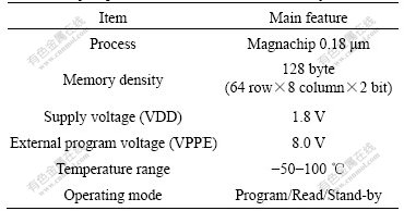
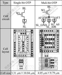
Fig.1 Circuits and layout plots of single-bit OTP cell and multi- bit OTP cell
The memory density is 1 kbit, viz. 64 row��8 column�� 2 bit. Two supply voltages are used: logic supply voltage VDD (=1.8 V) and external program voltage VPPE (= 8.0 V). There are two operating modes: program and read modes.
Since the body node of MOS capacitor that is antifuse in Fig.1 should be connected to the source node of cell access transistor, PMOS capacitor is used instead of NMOS capacitor. As shown in Fig.1, the designed multi-bit OTP cell consists of three low-voltage (LV) PMOS capacitors of 1.8 V having thin gate oxide as antifuse, and medium-voltage (MV) NMOS access transistor of 5 V having thick gate oxide. The gate node of the NMOS access transistor is connected to the word line (WL), the source node to BL, and the drain node to each top node of three PMOS capacitors. And each gate node of three PMOS capacitors is connected to each of three source lines (SLs) (SL_GND, SL_A0b, and SL_A0). The layout area of the multi-bit OTP cell grows about 13% larger than that of a single-bit OTP cell.
As shown in Fig.2, the designed 1 kbit OTP memory consists of an OTP cell array of 64 row��8 column, VPP switching circuit, row decoder selecting one of 64 WLs by decoding the row address bus RA[5:0], SL driver, RD S/A (read data sense amplifier), and control logic. A two-bit datum is compressed and programmed into a unit cell. SL driver in Fig.2 drives with necessary bias voltage selecting one SL out of SL_GND, SL_A0b, and SL_A0 using lower byte WD_LB and upper byte WD_UB. And the control logic supplies internal control signals suitable for program and read modes according to control signals (CE, READ, PGM, and RSTb). There are two operation modes: program and read. The operation mode is determined by the control signals. We add ��b�� at the end of signal name if the signal is asserted to be low. Here ��b�� means bar.
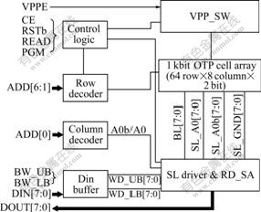
Fig.2 Block diagram of 1 kbit OTP memory
The lower byte and upper byte to be programmed are written into the DIN buffer using signals BW_LB (lower byte write) and BW_UB (upper byte write) in program mode, as shown in Fig.3. The two-byte write data WD[15:0] in Fig.2 drives SL_GND[7:0], SL_A0b[7:0], and SL_A0[7:0] according to the compressed data by the SL driver when program signal PGM is activated with high signal. Table 5 shows driving voltages of SL_GND, SL_A0b, and SL_A0 and broken antifuses according to data patterns in program mode. BL[7:0] keeps 0 V in program mode and so antifuses applied with VPP break down and short electrically. And antifuses in floating state keep open state. Fig.4 shows an equivalent circuit of four cells when the compressed data in Table 3 are programmed, where resistor means that antifuse shorted electrically by oxide breaks down. The programming time of the proposed OTP memory is nearly 50% smaller than that of the conventional counterpart since two consecutive bytes can be programmed into eight OTP cells at a time by compressing in program mode for the proposed OTP memory. Buffer write times by BW_LB and BW_UB are negligibly smaller than the programming time, as shown in Fig.3.
Signals chip enable (CE) and READ are activated after address A[6:0] to be read out from is applied in read mode, as shown in Fig.5. If a read operation performs, BL is precharged to VDD and then WL selected by the row address A[6:1] is applied with VDD. SL_GND, SL_A0b, and SL_A0 are biased by the column address A0, as shown in Table 6. Bias voltages of four cells compressed according to A0 in read mode are shown in Fig.6, indicating that the programmed data of Table 1 are read out. The read data appear on the port DOUT in access time after control signal READ is applied. And PGM and RSTb keep 0 V, and VDD and DIN are in don��t-care state.
In the VPP switching circuit of Fig.7, VPP drives
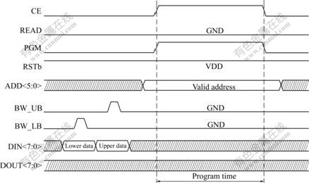
Fig.3 Timing diagram in program mode
Table 5 Driving voltages of SL_GND, SL_A0b, and SL_A0 and broken antifuses according to data patterns in program mode

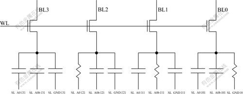
Fig.4 Equivalent circuit of four cells when compressed data in Table 3 are programmed
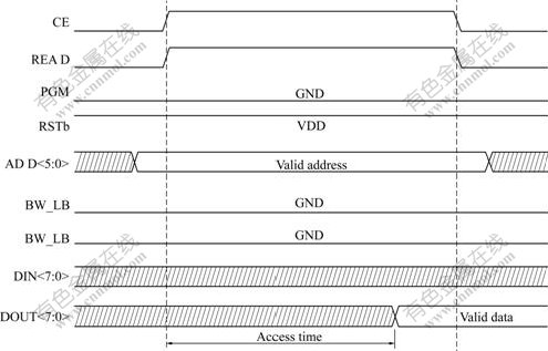
Fig.5 Timing diagram in read mode
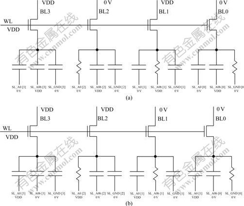
Fig.6 Bias voltages of WL, BL, and SL for four cells in read mode: (a) In case of A0 is 0; (b) In case of A0 is 1
Table 6 Driving voltages of SL_GND, SL_A0b, and SL_A0 according to A0 in read mode

with VPPE (=8.0 V) since signal PGM_ENb is enabled with 0 V, MP1 turns on, and MP2 turns off in program mode. And VPP drives with VDD since signal PGM_ENb becomes VDD, MP1 turns off, and MP2 turns on in read mode. The driver circuit of Fig.8 drives with VPP for the selected WL and keeps 0 V for the non-selected WLs, since signal CELLACC goes high and the row address bus A[6:1] is decoded in entering program or read mode. The SL driver circuit of each column consists of three circuits: SL_GND, SL_A0b, and SL_A0, as shown in Fig.9.

Fig.7 Schematic diagram of VPP switching circuit
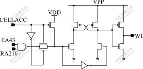
Fig.8 Schematic diagram of WL driver circuit
For the designed OTP memory, a datum can be read out and programmed byte by byte. And the circuit is simplified by using the sense amplifier of clocked inverter type of Fig.10 instead of current sense amplifier in read mode [15]. Since switch MN1 turns on in read mode, BL and DLINE are connected electrically. And since MP0 and MP1 are turned on by a short pulse of signal PRECHARGE before WL is activated, DLINE and BL are all precharged to voltage of VDD. Signal SAENb (sense amplifier enable) is enabled with 0 V, after cell datum is developed on BL with WL activated as shown in Fig.8. The sense amplifier of clocked inverter type outputs a read datum to DOUT by sensing if DLINE is VDD or 0 V when signal SAENb is enabled with 0 V after the read datum on DLINE is developed sufficiently. Since PMOS load transistor MP2 with high impedance turns on while WL is selected, it acts as a load pulling DLINE up to VDD such that DLINE is not discharged by off leakage current when datum ��1�� is read.
3 Simulation results
A multi-bit 1 kbit OTP memory is designed with 0.18 ��m CMOS process in this work. Fig.11 shows a timing diagram for the control signals CE and READ from the OTP memory in read mode, and the signal PRECHARGE, DLINE_LOADb, and SAENb from the control logic of Fig.2. DLINE and BL are precharged to
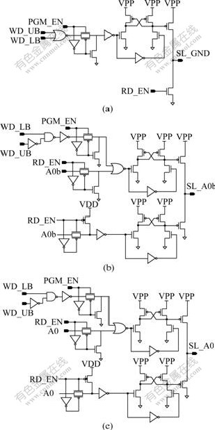
Fig.9 Driver circuits of (a) SL_GND, (b) SL_A0b, and (c) SL_A0
voltage VDD by the signal PRECHARGE as shown in Fig. 10 when a read command enters. If WL is activated and a cell datum is transferred to BL after BL is precharged, the read datum of DLINE is sensed by the BL S/A and output to node DOUT by signal SAENb. Fig.11(a) shows a SPICE simulation result for a ��0��-programmed cell and Fig.11(b) does for a ��1��-programmed cell. The read current is simulated to be 30.4 ��A under the following condition: read cycle time 1 ��s, VDD 1.8 V, and temperature 25 ��.
The layout area is 235 ��m��452 ��m for the single- bit memory and 214 ��m��327 ��m for the multi-bit memory. The layout area of the multi-bit OTP memory is 34% smaller than that of the single-bit counterpart.

Fig.10 Schematic diagram of clocked inverter-type sense amplifier
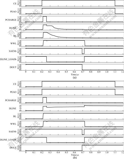
Fig.11 Simulation results in read mode: (a) In case that ��0�� is programmed in cell; (b) In case that ��1�� is programmed in cell (vertical axes represent signal voltages, V)
4 Conclusions
(1) A conventional OTP cell can store a datum of single bit per cell. On the contrary, a multi-bit OTP cell that can compress and store a two-bit per cell is newly developed, where a unit cell consists of an access transistor and three PMOS capacitors as antifuses. Although multi-bit OTP cell size is 13% larger than the conventional OTP cell size, the layout area of the proposed OTP memory can be smaller since the sizes of cell array and row decoder are smaller. The layout area of the proposed OTP memory is 214 ��m��327 ��m, which is 34% smaller than that of the conventional single-bit OTP memory.
(2) The programming time of the proposed OTP memory is nearly 50% smaller than that of the conventional counterpart since two consecutive bytes can be programmed into eight OTP cells at a time by compressing in program mode.
References
[1] ALAVI M, BOHR M, HICKS J, DENHAM M, CASSENS A, DOUGLAS D, TSAI M C. A PROM element based on salicide agglomeration of poly fuses in a CMOS logic process [C]// Proceedings of IEEE Electron Devices Meeting. Washington, 1997: 855-858.
[2] LIM K N, KANG S S, CHOI J H, JOO J H, LEE Y S, LEE J S, CHO S I, RYU B G. Bit line coupling scheme and electrical fuse circuit for reliable operation of high density DRAM [C]// Proceedings of Symposium on VLSI Circuits. Kyoto, 2001: 33-34.
[3] KPTHANDARAMAN C, IYER S K, IYER S S. Electrically programmable fuse (efuse) using electromigration in silicides [J]. IEEE Electron Device Letters, 2002, 23(9): 523-525.
[4] FELLNER J, BOESMUELLER P, REITER H. Lifetime study for a poly fuse in a 0.35 mm polycide CMOS process [C]// Proceedings of IEEE the 43rd Annual International Reliability Physics Symposium. San Jose, 2005: 446-449.
[5] FELLNER J, PREMSTAETTEN S. A one time programming cell using more than two resistance levels of a polyfuse [C]// Proceedings of IEEE Custom Integrated Circuits Conference. San Jose, 2005: 263-266.
[6] MIN B J, LEE K W, LEE H J, KIM S R, OH S G, JEON B G, YANG H H, KIM M K, CHO S H, CHEONG H S, CHUNG C H, KIM K N. An embedded non-volatile FRAM with electrical fuse repair scheme and one-time programming scheme for high performance smart cards [C]// Proceedings of IEEE Custom Integrated Circuits Conference. San Jose, 2005: 255-258.
[7] UEDA T, TAKAOKA H, HAMADA M, KOBAYASHI Y, ONO A. A novel Cu electrical fuse structure and blowing scheme utilizing crack-assisted mode for 90-45 nm-node and beyond [C]// Proceedings of Symposium on VLSI Technology. Hawaii, 2006: 138-139.
[8] SAFRAN J, LESLIE A, FREDEMAN G, KOTHANDARAMAN C, CESTERO A, CHEN X, RAJEEVAKUMAR R, KIM D K, LI Y Z, MOY D, ROBSON N, KIRIHATA T, IYER S. A compact efuse programmable array memory for SOI CMOS [C]// Proceedings of Symposium on VLSI Circuits. Kyoto, 2007: 72-73.
[9] ROBSON N, SAFRAN J, KOTHANDARAMAN C, CESTERO A, CHEN X, RAJEEVAKUMAR R, LESLIE A, MOY D, KIRIHATA T, IYER S. Electrically programmable fuse (efuse): From memory redundancy autonomic chips [C]// Proceedings of IEEE Custom Integrated Circuits Conference. San Jose, 2007: 799-804.
[10] CHOI J S, WEE J K, CHO H Y, KIM P J, OH J K, LEE C H, CHUNG J Y, KIM S J, YANG W. Antifuse EPROM circuit for field programmable DRAM [C]// Proceedings of IEEE International Solid-State Circuits Conference. San Francisco, 2000: 406-407.
[11] CHA H K, YUN I H, KIM J B, SO B C, CHUN K H, NAM I K, LEE K R. A 32-KB standard CMOS antifuse one-time programmable ROM embedded in a 16-bit microcontroller [J]. IEEE Journal of Solid-State Circuits, 2006, 41(9): 2115-2124.
[12] BARSATAN R, MAN T Y, CHAN M S. A zero mask one-time programmable memory array for RFID applications [C]// Proceedings of IEEE International Symposium on Circuits and Systems. Island of Kos, 2006: 975-978.
[13] MATSUFUJI K, NAMEKAWA T, NAKANO H, ITO H, WADA O, OTSUKA N. A 65 nm pure CMOS one-time programmable memory using a two-port antifuse cell implemented in a matrix structure [C]// Proceedings of IEEE Asian Solid-State Circuit Conference. Jeju, 2007: 212-215.
[14] LI L Z, KIM T H, SHIM O Y, PARK M H, HA P B, KIM Y H. Design of synchronous 256-bit OTP memory [J]. KIMICS of Semiconductors and Communications, 2008, 12(7): 1227-1234.
[15] LEE J H, KIM J H, LIM G H, KIM T H, LEE J H, PARK K H, PARK M H, HA P B, KIM Y H. Low-power 512-bit EEPROM designed for UHF RFID tag chip [J]. ETRI Journal, 2008, 30(3): 347-354.
(Edited by CHEN Wei-ping)
Foundation item: Project supported by the 2nd Stage of Brain Korea; Project supported by the Korea Research Foundation
Received date: 2008-09-17; Accepted date: 2008-12-20
Corresponding author: KIM Y H, Professor, PhD; Tel: +82-55-2851023; E-mail: youngkim@changwon.ac.kr
- Design of small-area multi-bit antifuse-type 1 kbit OTP memory


